

Ebyte E01 Series, E01-ML01D, E01-ML01DP4, E01-ML01DP5, E01-2G4M27D User Manual
...
nRF24L01P Wireless Module
E01 Series
This manual may be modified based on product upgrade, please refer to the latest version.
All rights to interpret and modify this manual belong to Chengdu Ebyte Electronic Technology Co., Ltd.
User Manual
nRF24L01P wireless module E01 series user manual
Copyright ©2012–2017,Chengdu Ebyte Electronic Technology Co.,Ltd.
1
Version
Date
Description
Issued by
1.00
2017/11/15
Initial version
huaa
1.10
2018/5/22
Added contents
huaa
1.20
2018/8/13
Added E01 (2G4M27D)
Huaa
Brief Introduction
E01 series 2.4Ghz wireless transceiver module based on nRF24L01P with SPI interface features small size and various application usage.
E01 series modules are embedded with imported electronic parts, such as industrial crystals with high precision and TCXO. With built-in PA and LNA, the
20dBm module has better performance for communication and operating range; 0dBm modules with imported parts owns excellent RF performance, especially
popular among users who require low power consumption.
E01 series strictly stick to the design rules home and abroad of FCC, CE, CCC and meet the related RF certifications and export standards. As hardware
platform,users need to carry out secondary development.
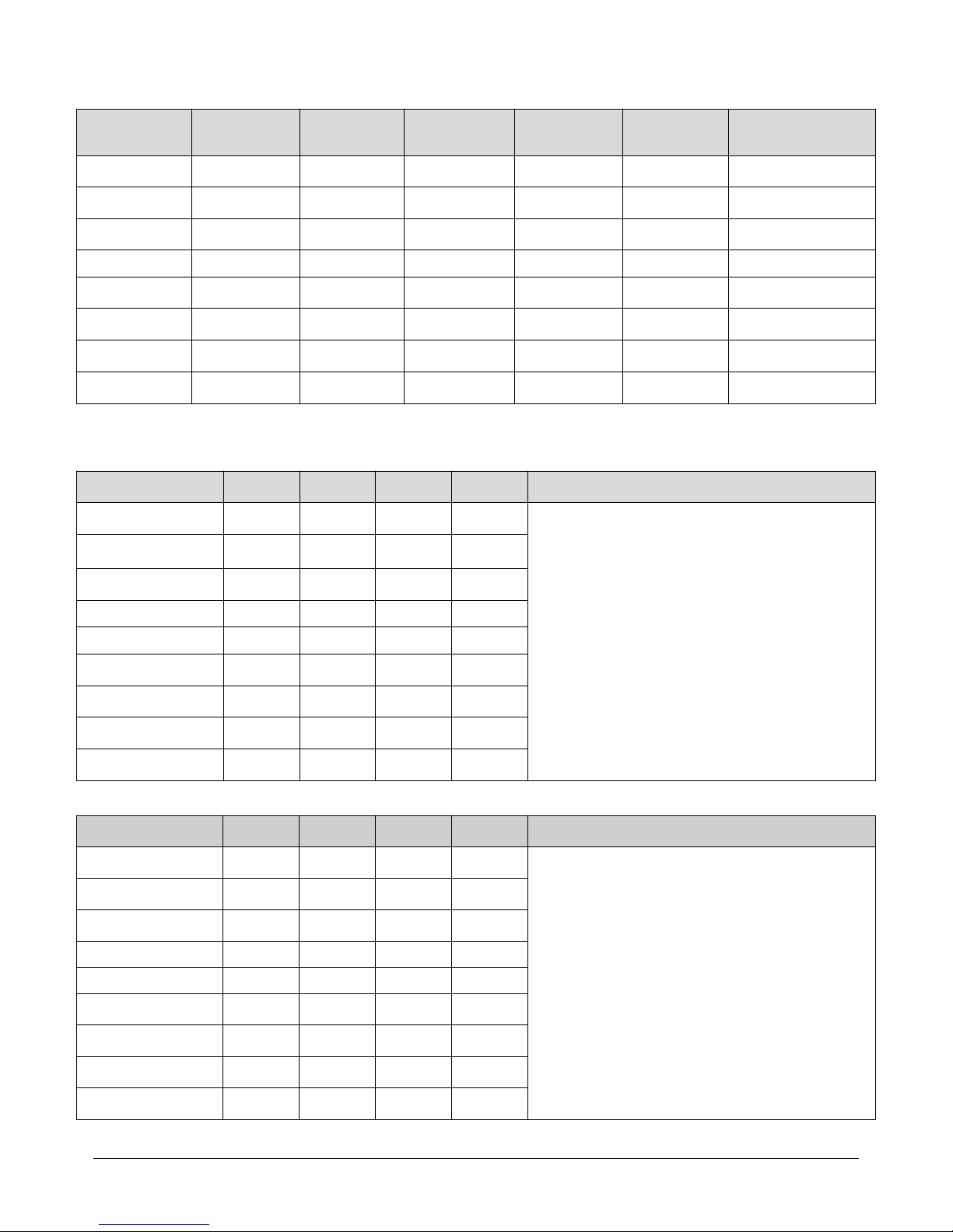
Model
Antenna
Packing
Transmitting power
Distance
E01-ML01D
PCB
DIP
0dBm
100m
E01-ML01DP4
PCB
DIP
20dBm
1800m
E01-ML01DP5
SMA-K
DIP
20dBm
2500m
E01-2G4M27D
SMA-K
DIP
27dBm
3500m
E01-ML01IPX
IPEX
SMD
0dBm
200m
E01-ML01S
PCB
SMD
0dBm
100m
E01-ML01SP2
PCB/ IPEX
SMD
20dBm
1500m
E01-ML01SP4
IPEX
SMD
20dBm
2000m

nRF24L01P wireless module E01 series user manual
Copyright ©2012–2017,Chengdu Ebyte Electronic Technology Co.,Ltd.
2
Contents
1. Technical Parameter
........................................................................................................................................................................
3
1.1. General parameter
..................................................................................................................................................................
3
1.2. Electrical parameter
................................................................................................................................................................
3
1.2.1. Transmitting current
......................................................................................................................................................
3
1.2.2. Receiving current
...........................................................................................................................................................
3
1.2.3. Turn-off current
.............................................................................................................................................................
4
1.2.4. Voltage supply
...............................................................................................................................................................
4
1.2.5. Communication level
.....................................................................................................................................................
4
1.3. RF parameter
...........................................................................................................................................................................
5
1.3.1. Transmitting power
.......................................................................................................................................................
5
1.3.2. Receiving sensitivity
.......................................................................................................................................................
5
1.3.3. Recommended operating frequency
...........................................................................................................................
5
1.4. Tested distance
.......................................................................................................................................................................
6
2. Mechanical Characteristics
..............................................................................................................................................................
6
2.1. E01-ML01D
.............................................................................................................................................................................
6
2.2. E01-ML01DP4
.........................................................................................................................................................................
7
2.3. E01-ML01DP5
.........................................................................................................................................................................
8
2.4. E01-2G4M27D
........................................................................................................................................................................
9
2.5. E01-ML01IPX
........................................................................................................................................................................
10
2.6. E01-ML01S
............................................................................................................................................................................
11
2.7. E01-ML01SP2
.......................................................................................................................................................................
12
2.8. E01-ML01SP4
.......................................................................................................................................................................
13
3. Recommended Circuit Diagram
...................................................................................................................................................
14
4. Electrical Parameters
.....................................................................................................................................................................
14
5. Antenna Type
.................................................................................................................................................................................
16
6. Notes
..............................................................................................................................................................................................
16
7. Production Guidance
....................................................................................................................................................................
17
7.1. Reflow Soldering Temperature
...........................................................................................................................................
17
7.2. Reflow Curving Diagram
......................................................................................................................................................
17
8. FAQ
.................................................................................................................................................................................................
18
8.1. Communication range is too short
.....................................................................................................................................
18
8.2. Module is easy to damage
..................................................................................................................................................
18
9. Important Notes
............................................................................................................................................................................
18
10. About Us
......................................................................................................................................................................................
18
nRF24L01P wireless module E01 series user manual
Copyright ©2012–2017,Chengdu Ebyte Electronic Technology Co.,Ltd.
3
1. Technical Parameter
1.1. General parameter
Model
Core IC
Size
Net Weight
Operating
Temperature
Operating
Humidity
Storage
Temperature
E01-ML01D
nRF24L01P
12.6 * 22.6 mm
1.1±0.1g
-40 ~ 85°C
10% ~ 90%
-40 ~ 125°C
E01-ML01DP4
nRF24L01P
15 * 27 mm
1.4±0.1g
-40 ~ 85°C
10% ~ 90%
-40 ~ 125°C
E01-ML01DP5
nRF24L01P
18 * 33.4 mm
4.9±0.1g
-40 ~ 85°C
10% ~ 90%
-40 ~ 125°C
E01-2G4M27D
nRF24L01P
18 * 33.4 mm
5.1±0.1g
-40 ~ 85°C
10% ~ 90%
-40 ~ 125°C
E01-ML01IPX
nRF24L01P
12 * 19 mm
0.6±0.1g
-40 ~ 85°C
10% ~ 90%
-40 ~ 125°C
E01-ML01S
nRF24L01P
12 * 19 mm
0.5±0.1g
-40 ~ 85°C
10% ~ 90%
-40 ~ 125°C
E01-ML01SP2
nRF24L01P
12.8 * 25 mm
0.8±0.1g
-40 ~ 85°C
10% ~ 90%
-40 ~ 125°C
E01-ML01SP4
nRF24L01P
14.8 * 18 mm
1.2±0.1g
-40 ~ 85°C
10% ~ 90%
-40 ~ 125°C
1.2. Electrical parameter
1.2.1. Transmitting current
Model
Min
Typ
Max
Unit
Remarks
E01-ML01D
121314
mA
●When designing current supply circuit, 30% margin is recommended
to be remained so as to ensure long-term stable operation of the
whole module;
●The current at the instant of transmitting may be high, but the total
energy consumed may be lower due to very short transmitting time;
●When using external antenna, the impedance matching degree at
different frequency points between antenna and module may affect
the transmitting current value at different levels.
E01-ML01DP4
100
110
120
mA
E01-ML01DP5
120
130
140
mA
E01-2G4M27D@3.3V
480
490
500
mA
E01-2G4M27D@5.0V
380
390
400
mA
E01-ML01IPX
121314
mA
E01-ML01S121314mA
E01-ML01SP2
120
130
140
mA
E01-ML01SP4
110
120
130
mA
1.2.2. Receiving current
Model
Min
Typ
Max
Unit
Remarks
E01-ML01D
111213
mA
●The current consumed when the RF chip is only working at receiving
mode is called as receiving current,the tested receiving current may
be higher for some RF chips with communication protocol or the
developers have loaded their own protocol to the whole module;
● The current at pure receiving mode will be mA level, users can
realize µA level of receiving current through firmware development.
E01-ML01DP4
182022
mA
E01-ML01DP5
182022
mA
E01-2G4M27D@3.3V
222324
mA
E01-2G4M27D@5.0V
212223
mA
E01-ML01IPX
111213
mA
E01-ML01S111213mA
E01-ML01SP2
192123
mA
E01-ML01SP4
242628
mA
nRF24L01P wireless module E01 series user manual
Copyright ©2012–2017,Chengdu Ebyte Electronic Technology Co.,Ltd.
4
1.2.3. Turn-off current
Model
Min
Typ
Max
Unit
Remarks
E01-ML01D
0.5
1.0
2.0
µA
● The turn-off current means the current consumed by CPU, RAM,
Clock and some registers which remain operating. SoC is at very low
power consumption status;
● The turn-off current is always lower than the current consumed
when the power supply source of the whole module is at no-load
status.
E01-ML01DP4
0.5
1.0
2.0
µA
E01-ML01DP5
0.5
1.0
2.0
µA
E01-2G4M27D
450
455
460
µA
E01-ML01IPX
0.5
1.0
2.0
µA
E01-ML01S
0.5
1.0
2.0
µA
E01-ML01SP2
0.5
1.0
2.0
µA
E01-ML01SP4
0.5
1.0
2.0
µA
1.2.4. Voltage supply
Model
Min
Typ
Max
Unit
Remarks
E01-ML01D
2.0
3.3
3.6
V DC
●If the module stays at maximum voltage for a long time, it may be
damaged;
● The power supply pin has certain surge-resistance ability, but the
potential pulse is higher than the maximum power supply voltage;
●The power supply is not advisable to be below 3.0V, or the RF
parameters will be influenced at different degree.
● For max 30dBm, voltage is no less than 4.75V,or RF parameters
will be affected to different extend.
E01-ML01DP4
2.0
3.3
3.6
V DC
E01-ML01DP5
2.0
3.3
3.6
V DC
E01-2G4M27D
2.5
3.3
5.5
V DC
E01-ML01IPX
2.0
3.3
3.6
V DC
E01-ML01S
2.0
3.3
3.6
V DC
E01-ML01SP2
2.0
3.3
3.6
V DC
E01-ML01SP4
2.0
3.3
3.6
V DC
1.2.5. Communication level
Model
Min
Typ
Max
Unit
Remarks
E01-ML01D
2.0
3.3
3.6
V DC
● If the module stays at maximum communication level for a long
time, it may be damaged;
●The module is compatible with some 5.0V MCU; Because there’s too
much model, pls refer to the real testing or consult our sales;
● There are various ways to switch communication level, but it will
affect the whole power consumption to a large extend.
E01-ML01DP4
2.0
3.3
3.6
V DC
E01-ML01DP5
2.0
3.3
3.6
V DC
E01-2G4M27D
2.0
3.3
3.6
V DC
E01-ML01IPX
2.0
3.3
3.6
V DC
E01-ML01S
2.0
3.3
3.6
V DC
E01-ML01SP2
2.0
3.3
3.6
V DC
E01-ML01SP4
2.0
3.3
3.6
V DC
nRF24L01P wireless module E01 series user manual
Copyright ©2012–2017,Chengdu Ebyte Electronic Technology Co.,Ltd.
5
1.3. RF parameter
1.3.1. Transmitting power
Model
Min
Typ
Max
Unit
Remarks
E01-ML01D
-0.200.3
dBm
● Due to the error of the materials, each LRC component has ± 0.1%
error, so error accumulation will occur since multiple LRC
components are used in the whole RF circuit, and the transmitting
currents will be different at different modules;
● The power consumption can be lowered by lowering the
transmitting power, but the efficiency of the internal PA will be
decreased by lowering transmitting power due to various reasons;
● The transmitting power will be lowered by lowering the power
supply voltage.
E01-ML01DP4
19.72020.4
dBm
E01-ML01DP5
19.72020.4
dBm
E01-2G4M27D
26.52727.5
dBm
E01-ML01IPX
-0.200.3
dBm
E01-ML01S
-0.200.3
dBm
E01-ML01SP2
19.72020.4
dBm
E01-ML01SP4
19.72020.4
dBm
1.3.2. Receiving sensitivity
Model
Min
Typ
Max
Unit
Remarks
E01-ML01D
-92.0
-93.0
-94.0
dBm
● The sensitivity is tested under the air data rate 250kbps;
● Due to the error of the materials, each LRC component has ± 0.1%
error, so error accumulation will occur since multiple LRC
components are used in the whole RF circuit, and the transmitting
currents will be different at different modules;
●The receiving sensitivity will be reduced and communication range
will be shortened while increasing the air data rate.
E01-ML01DP4
-95.5
-96.0
-97.5
dBm
E01-ML01DP5
-95.5
-96.0
-97.5
dBm
E01-2G4M27D
-98.0
-99.0
-100.0
dBm
E01-ML01IPX
-92.0
-93.0
-94.0
dBm
E01-ML01S
-92.0
-93.0
-94.0
dBm
E01-ML01SP2
-95.5
-96.0
-97.5
dBm
E01-ML01SP4
-95.5
-96.0
-97.5
dBm
1.3.3. Recommended operating frequency
Model
Min
Typ
Max
Unit
Remarks
E01-ML01D
2400
2430
2525
MHz
● To work within the recommended frequency can assure the modules
to meet all the parameters;
● It is recommended to avoid the crowded integral frequency such as
433.0MHz, 868.0MHz, 915MHz, 240MHz etc.
E01-ML01DP4
2400
2430
2525
MHz
E01-ML01DP5
2400
2430
2525
MHz
E01-2G4M27D
2400
2430
2525
MHz
E01-ML01IPX
2400
2430
2525
MHz
E01-ML01S
2400
2430
2525
MHz
E01-ML01SP2
2400
2430
2525
MHz
E01-ML01SP4
2400
2430
2525
MHz
 Loading...