

Page 1

nRF24L01P Wireless Module
E01 Series
This manual may be modified based on product upgrade, please refer to the latest version.
All rights to interpret and modify this manual belong to Chengdu Ebyte Electronic Technology Co., Ltd.
User Manual
Page 2
nRF24L01P wireless module E01 series user manual
Copyright ©2012–2017,Chengdu Ebyte Electronic Technology Co.,Ltd.
1
Version
Date
Description
Issued by
1.00
2017/11/15
Initial version
huaa
1.10
2018/5/22
Added contents
huaa
1.20
2018/8/13
Added E01 (2G4M27D)
Huaa
Brief Introduction
E01 series 2.4Ghz wireless transceiver module based on nRF24L01P with SPI interface features small size and various application usage.
E01 series modules are embedded with imported electronic parts, such as industrial crystals with high precision and TCXO. With built-in PA and LNA, the
20dBm module has better performance for communication and operating range; 0dBm modules with imported parts owns excellent RF performance, especially
popular among users who require low power consumption.
E01 series strictly stick to the design rules home and abroad of FCC, CE, CCC and meet the related RF certifications and export standards. As hardware
platform,users need to carry out secondary development.
Model
Antenna
Packing
Transmitting power
Distance
E01-ML01D
PCB
DIP
0dBm
100m
E01-ML01DP4
PCB
DIP
20dBm
1800m
E01-ML01DP5
SMA-K
DIP
20dBm
2500m
E01-2G4M27D
SMA-K
DIP
27dBm
3500m
E01-ML01IPX
IPEX
SMD
0dBm
200m
E01-ML01S
PCB
SMD
0dBm
100m
E01-ML01SP2
PCB/ IPEX
SMD
20dBm
1500m
E01-ML01SP4
IPEX
SMD
20dBm
2000m
Page 3

nRF24L01P wireless module E01 series user manual
Copyright ©2012–2017,Chengdu Ebyte Electronic Technology Co.,Ltd.
2
Contents
1. Technical Parameter
........................................................................................................................................................................
3
1.1. General parameter
..................................................................................................................................................................
3
1.2. Electrical parameter
................................................................................................................................................................
3
1.2.1. Transmitting current
......................................................................................................................................................
3
1.2.2. Receiving current
...........................................................................................................................................................
3
1.2.3. Turn-off current
.............................................................................................................................................................
4
1.2.4. Voltage supply
...............................................................................................................................................................
4
1.2.5. Communication level
.....................................................................................................................................................
4
1.3. RF parameter
...........................................................................................................................................................................
5
1.3.1. Transmitting power
.......................................................................................................................................................
5
1.3.2. Receiving sensitivity
.......................................................................................................................................................
5
1.3.3. Recommended operating frequency
...........................................................................................................................
5
1.4. Tested distance
.......................................................................................................................................................................
6
2. Mechanical Characteristics
..............................................................................................................................................................
6
2.1. E01-ML01D
.............................................................................................................................................................................
6
2.2. E01-ML01DP4
.........................................................................................................................................................................
7
2.3. E01-ML01DP5
.........................................................................................................................................................................
8
2.4. E01-2G4M27D
........................................................................................................................................................................
9
2.5. E01-ML01IPX
........................................................................................................................................................................
10
2.6. E01-ML01S
............................................................................................................................................................................
11
2.7. E01-ML01SP2
.......................................................................................................................................................................
12
2.8. E01-ML01SP4
.......................................................................................................................................................................
13
3. Recommended Circuit Diagram
...................................................................................................................................................
14
4. Electrical Parameters
.....................................................................................................................................................................
14
5. Antenna Type
.................................................................................................................................................................................
16
6. Notes
..............................................................................................................................................................................................
16
7. Production Guidance
....................................................................................................................................................................
17
7.1. Reflow Soldering Temperature
...........................................................................................................................................
17
7.2. Reflow Curving Diagram
......................................................................................................................................................
17
8. FAQ
.................................................................................................................................................................................................
18
8.1. Communication range is too short
.....................................................................................................................................
18
8.2. Module is easy to damage
..................................................................................................................................................
18
9. Important Notes
............................................................................................................................................................................
18
10. About Us
......................................................................................................................................................................................
18
Page 4
nRF24L01P wireless module E01 series user manual
Copyright ©2012–2017,Chengdu Ebyte Electronic Technology Co.,Ltd.
3
1. Technical Parameter
1.1. General parameter
Model
Core IC
Size
Net Weight
Operating
Temperature
Operating
Humidity
Storage
Temperature
E01-ML01D
nRF24L01P
12.6 * 22.6 mm
1.1±0.1g
-40 ~ 85°C
10% ~ 90%
-40 ~ 125°C
E01-ML01DP4
nRF24L01P
15 * 27 mm
1.4±0.1g
-40 ~ 85°C
10% ~ 90%
-40 ~ 125°C
E01-ML01DP5
nRF24L01P
18 * 33.4 mm
4.9±0.1g
-40 ~ 85°C
10% ~ 90%
-40 ~ 125°C
E01-2G4M27D
nRF24L01P
18 * 33.4 mm
5.1±0.1g
-40 ~ 85°C
10% ~ 90%
-40 ~ 125°C
E01-ML01IPX
nRF24L01P
12 * 19 mm
0.6±0.1g
-40 ~ 85°C
10% ~ 90%
-40 ~ 125°C
E01-ML01S
nRF24L01P
12 * 19 mm
0.5±0.1g
-40 ~ 85°C
10% ~ 90%
-40 ~ 125°C
E01-ML01SP2
nRF24L01P
12.8 * 25 mm
0.8±0.1g
-40 ~ 85°C
10% ~ 90%
-40 ~ 125°C
E01-ML01SP4
nRF24L01P
14.8 * 18 mm
1.2±0.1g
-40 ~ 85°C
10% ~ 90%
-40 ~ 125°C
1.2. Electrical parameter
1.2.1. Transmitting current
Model
Min
Typ
Max
Unit
Remarks
E01-ML01D
121314
mA
●When designing current supply circuit, 30% margin is recommended
to be remained so as to ensure long-term stable operation of the
whole module;
●The current at the instant of transmitting may be high, but the total
energy consumed may be lower due to very short transmitting time;
●When using external antenna, the impedance matching degree at
different frequency points between antenna and module may affect
the transmitting current value at different levels.
E01-ML01DP4
100
110
120
mA
E01-ML01DP5
120
130
140
mA
E01-2G4M27D@3.3V
480
490
500
mA
E01-2G4M27D@5.0V
380
390
400
mA
E01-ML01IPX
121314
mA
E01-ML01S121314mA
E01-ML01SP2
120
130
140
mA
E01-ML01SP4
110
120
130
mA
1.2.2. Receiving current
Model
Min
Typ
Max
Unit
Remarks
E01-ML01D
111213
mA
●The current consumed when the RF chip is only working at receiving
mode is called as receiving current,the tested receiving current may
be higher for some RF chips with communication protocol or the
developers have loaded their own protocol to the whole module;
● The current at pure receiving mode will be mA level, users can
realize µA level of receiving current through firmware development.
E01-ML01DP4
182022
mA
E01-ML01DP5
182022
mA
E01-2G4M27D@3.3V
222324
mA
E01-2G4M27D@5.0V
212223
mA
E01-ML01IPX
111213
mA
E01-ML01S111213mA
E01-ML01SP2
192123
mA
E01-ML01SP4
242628
mA
Page 5
nRF24L01P wireless module E01 series user manual
Copyright ©2012–2017,Chengdu Ebyte Electronic Technology Co.,Ltd.
4
1.2.3. Turn-off current
Model
Min
Typ
Max
Unit
Remarks
E01-ML01D
0.5
1.0
2.0
µA
● The turn-off current means the current consumed by CPU, RAM,
Clock and some registers which remain operating. SoC is at very low
power consumption status;
● The turn-off current is always lower than the current consumed
when the power supply source of the whole module is at no-load
status.
E01-ML01DP4
0.5
1.0
2.0
µA
E01-ML01DP5
0.5
1.0
2.0
µA
E01-2G4M27D
450
455
460
µA
E01-ML01IPX
0.5
1.0
2.0
µA
E01-ML01S
0.5
1.0
2.0
µA
E01-ML01SP2
0.5
1.0
2.0
µA
E01-ML01SP4
0.5
1.0
2.0
µA
1.2.4. Voltage supply
Model
Min
Typ
Max
Unit
Remarks
E01-ML01D
2.0
3.3
3.6
V DC
●If the module stays at maximum voltage for a long time, it may be
damaged;
● The power supply pin has certain surge-resistance ability, but the
potential pulse is higher than the maximum power supply voltage;
●The power supply is not advisable to be below 3.0V, or the RF
parameters will be influenced at different degree.
● For max 30dBm, voltage is no less than 4.75V,or RF parameters
will be affected to different extend.
E01-ML01DP4
2.0
3.3
3.6
V DC
E01-ML01DP5
2.0
3.3
3.6
V DC
E01-2G4M27D
2.5
3.3
5.5
V DC
E01-ML01IPX
2.0
3.3
3.6
V DC
E01-ML01S
2.0
3.3
3.6
V DC
E01-ML01SP2
2.0
3.3
3.6
V DC
E01-ML01SP4
2.0
3.3
3.6
V DC
1.2.5. Communication level
Model
Min
Typ
Max
Unit
Remarks
E01-ML01D
2.0
3.3
3.6
V DC
● If the module stays at maximum communication level for a long
time, it may be damaged;
●The module is compatible with some 5.0V MCU; Because there’s too
much model, pls refer to the real testing or consult our sales;
● There are various ways to switch communication level, but it will
affect the whole power consumption to a large extend.
E01-ML01DP4
2.0
3.3
3.6
V DC
E01-ML01DP5
2.0
3.3
3.6
V DC
E01-2G4M27D
2.0
3.3
3.6
V DC
E01-ML01IPX
2.0
3.3
3.6
V DC
E01-ML01S
2.0
3.3
3.6
V DC
E01-ML01SP2
2.0
3.3
3.6
V DC
E01-ML01SP4
2.0
3.3
3.6
V DC
Page 6
nRF24L01P wireless module E01 series user manual
Copyright ©2012–2017,Chengdu Ebyte Electronic Technology Co.,Ltd.
5
1.3. RF parameter
1.3.1. Transmitting power
Model
Min
Typ
Max
Unit
Remarks
E01-ML01D
-0.200.3
dBm
● Due to the error of the materials, each LRC component has ± 0.1%
error, so error accumulation will occur since multiple LRC
components are used in the whole RF circuit, and the transmitting
currents will be different at different modules;
● The power consumption can be lowered by lowering the
transmitting power, but the efficiency of the internal PA will be
decreased by lowering transmitting power due to various reasons;
● The transmitting power will be lowered by lowering the power
supply voltage.
E01-ML01DP4
19.72020.4
dBm
E01-ML01DP5
19.72020.4
dBm
E01-2G4M27D
26.52727.5
dBm
E01-ML01IPX
-0.200.3
dBm
E01-ML01S
-0.200.3
dBm
E01-ML01SP2
19.72020.4
dBm
E01-ML01SP4
19.72020.4
dBm
1.3.2. Receiving sensitivity
Model
Min
Typ
Max
Unit
Remarks
E01-ML01D
-92.0
-93.0
-94.0
dBm
● The sensitivity is tested under the air data rate 250kbps;
● Due to the error of the materials, each LRC component has ± 0.1%
error, so error accumulation will occur since multiple LRC
components are used in the whole RF circuit, and the transmitting
currents will be different at different modules;
●The receiving sensitivity will be reduced and communication range
will be shortened while increasing the air data rate.
E01-ML01DP4
-95.5
-96.0
-97.5
dBm
E01-ML01DP5
-95.5
-96.0
-97.5
dBm
E01-2G4M27D
-98.0
-99.0
-100.0
dBm
E01-ML01IPX
-92.0
-93.0
-94.0
dBm
E01-ML01S
-92.0
-93.0
-94.0
dBm
E01-ML01SP2
-95.5
-96.0
-97.5
dBm
E01-ML01SP4
-95.5
-96.0
-97.5
dBm
1.3.3. Recommended operating frequency
Model
Min
Typ
Max
Unit
Remarks
E01-ML01D
2400
2430
2525
MHz
● To work within the recommended frequency can assure the modules
to meet all the parameters;
● It is recommended to avoid the crowded integral frequency such as
433.0MHz, 868.0MHz, 915MHz, 240MHz etc.
E01-ML01DP4
2400
2430
2525
MHz
E01-ML01DP5
2400
2430
2525
MHz
E01-2G4M27D
2400
2430
2525
MHz
E01-ML01IPX
2400
2430
2525
MHz
E01-ML01S
2400
2430
2525
MHz
E01-ML01SP2
2400
2430
2525
MHz
E01-ML01SP4
2400
2430
2525
MHz
Page 7

nRF24L01P wireless module E01 series user manual
Copyright ©2012–2017,Chengdu Ebyte Electronic Technology Co.,Ltd.
6
1.4. Tested distance
Model
Min
Typ
Max
Unit
Remarks
E01-ML01D
90
100
110
m
●The external antenna used is of 5dBi gain and vertical polarization. The
height is 2.5 meters;
●The interval between each data packet is 2s, sending 100 packets with
30 bytes in each packet, the range at data lose rate of lower than 5% is
valid range;
●In order to obtain meaningful and reproducible results, we conducted
the tests in clear air with little electromagnetic interference at suburb
areas;
●Distance may be shorter with interference or obstacles.
E01-ML01DP4
1600
1800
1980
m
E01-ML01DP5
2300
2500
2800
m
E01-2G4M27D
3150
3500
3850
m
E01-ML01IPX
180
200
230
m
E01-ML01S
90
100
120
m
E01-ML01SP2
1300
1500
1600
m
E01-ML01SP4
1800
2000
2300
m
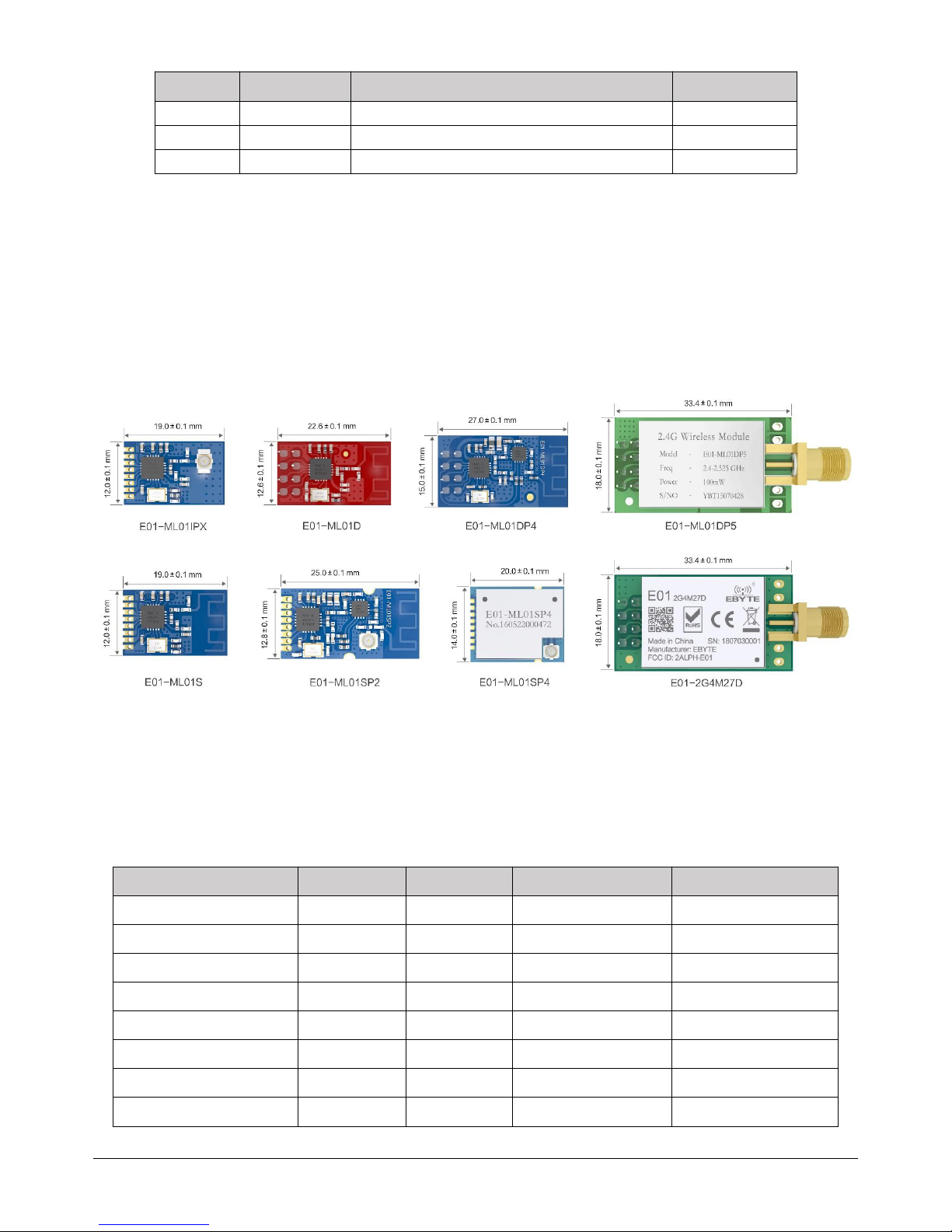
2. Mechanical Characteristics
2.1. E01-ML01D
Pin No.
Pin item
Pin direction
Pin application
1
GND
Ground
2
VCC
Power supply 1.9V~3.6V DC
3CEinput
Chip enable
4
CSN
input
SPI Chip select
5
SCK
input
SPI Clock
6
MOSI
input
SPI master output slave input
7
MISO
Output
SPI master input slave output
8
IRQ
Output
Interrupt request
★ Find more details on《nRF24L01P Datasheet》from Nordic ★
Page 8

nRF24L01P wireless module E01 series user manual
Copyright ©2012–2017,Chengdu Ebyte Electronic Technology Co.,Ltd.
7
2.2. E01-ML01DP4
Pin No.
Pin item
Pin direction
Pin application
1
GND
Ground,connect to power reference ground.
2
VCC
Power supply 2.0 V~3.6V DC
3
CE
input
Chip enable
4
CSN
input
SPI Chip select
5
SCK
input
SPI Clock
6
MOSI
input
SPI master output slave input
7
MISO
Output
SPI master input slave output
8
IRQ
Output
Interrupt request, valid in low communication level
★ Find more details on《nRF24L01P Datasheet》from Nordic ★
Page 9

nRF24L01P wireless module E01 series user manual
Copyright ©2012–2017,Chengdu Ebyte Electronic Technology Co.,Ltd.
8
2.3. E01-ML01DP5
Pin No.
Pin item
Pin direction
Pin application
1
GND
Ground
2
VCC
Power supply 2.0V~3.6V DC
3
CE
input
Chip enable
4
CSN
input
SPI Chip select
5
SCK
input
SPI Clock
6
MOSI
input
SPI master output slave input
7
MISO
Output
SPI master input slave output
8
IRQ
Output
Interrupt request, valid in low communication level
★ Find more details on《nRF24L01P Datasheet》from Nordic ★
Page 10

nRF24L01P wireless module E01 series user manual
Copyright ©2012–2017,Chengdu Ebyte Electronic Technology Co.,Ltd.
9
2.4. E01-2G4M27D
Pin No.
Pin item
Pin direction
Pin application
1
GND
Ground
2
VCC
Power supply 2.5V~5.5V DC, it’s recommended to use 3.3V.
3
CE
input
Chip enable
4
CSN
input
SPI Chip select
5
SCK
input
SPI Clock
6
MOSI
input
SPI master output slave input
7
MISO
Output
SPI master input slave output
8
IRQ
Output
Interrupt request, valid in low communication level
★ Find more details on《nRF24L01P Datasheet》from Nordic ★
Page 11

nRF24L01P wireless module E01 series user manual
Copyright ©2012–2017,Chengdu Ebyte Electronic Technology Co.,Ltd.
10
2.5. E01-ML01IPX
Pin No.
Pin item
Pin direction
Pin application
1
VCC
Power supply 1.9V~3.6V DC
2
CE
Input
Chip enable
3
CSN
Input
SPI Chip select
4
SCK
Input
SPI Clock
5
MOSI
Input
SPI master output slave input
6
MISO
Output
SPI master input slave output
7
IRQ
Output
Interrupt request, valid in low communication level
8
GND
Ground
★ Find more details on《nRF24L01P Datasheet》from Nordic ★
Page 12

nRF24L01P wireless module E01 series user manual
Copyright ©2012–2017,Chengdu Ebyte Electronic Technology Co.,Ltd.
11
2.6. E01-ML01S
Pin No.
Pin item
Pin direction
Pin application
1
VCC
Power supply 1.9V~3.6V DC
2
CE
Input
Chip enable
3
CSN
Input
SPI Chip select
4
SCK
Input
SPI Clock
5
MOSI
Input
SPI master output slave input
6
MISO
Output
SPI master input slave output
7
IRQ
Output
Interrupt request, valid in low communication level
8
GND
Ground
★ Find more details on《nRF24L01P Datasheet》from Nordic ★
Page 13

nRF24L01P wireless module E01 series user manual
Copyright ©2012–2017,Chengdu Ebyte Electronic Technology Co.,Ltd.
12
2.7. E01-ML01SP2
Pin No.
Pin item
Pin direction
Pin application
1
VCC
Power supply 2.0 V~3.6V DC
2
CE
Input
Chip enable
3
CSN
Input
SPI Chip select
4
SCK
Input
SPI Clock
5
MOSI
Input
SPI master output slave input
6
MISO
Output
SPI master input slave output
7
IRQ
Output
Interrupt request, valid in low communication level
8
GND
Ground
9
GND
Ground
10
GND
Ground
★ Find more details on《nRF24L01P Datasheet》from Nordic ★
Page 14

nRF24L01P wireless module E01 series user manual
Copyright ©2012–2017,Chengdu Ebyte Electronic Technology Co.,Ltd.
13
2.8. E01-ML01SP4
Pin No.
Pin item
Pin direction
Pin application
1
VCC
Power supply 2.0 V~3.6V DC
2
CE
Input
Chip enable
3
CSN
Input
SPI Chip select
4
SCK
Input
SPI Clock
5
MOSI
Input
SPI master output slave input
6
MISO
Output
SPI master input slave output
7
IRQ
Output
Interrupt request, valid in low communication level
8
GND
Ground
9
GND
Ground
10
GND
Ground
★ Find more details on《nRF24L01P Datasheet》from Nordic ★
Page 15

nRF24L01P wireless module E01 series user manual
Copyright ©2012–2017,Chengdu Ebyte Electronic Technology Co.,Ltd.
14
3. Recommended Circuit Diagram
No.
Brief introduction of connection between module and MCU (STM8)
1
CE pin can be high level for long-term, but it needs to set as POWER DOWN mode when the module writes registers, and it is
recommended that CE is controlled by MCU pin.
2
As interrupt pin for IRQ, it can be used to wake-up MCU and achieve fast response;
But the user can get the interrupt status through SPI (not recommended, it is not conducive to the overall power consumption, and with
low efficiency).
4. Electrical Parameters
In different power of nRF24L01P, the real transmitting power of E01-2G4M27D, 3.3V, as below:
Page 16

nRF24L01P wireless module E01 series user manual
Copyright ©2012–2017,Chengdu Ebyte Electronic Technology Co.,Ltd.
15
The real transmitting power of E01-2G4M27D in different voltage, testing under 2460MHz:
The corresponding register value of nRF24L01+transmitting power output:
Page 17

nRF24L01P wireless module E01 series user manual
Copyright ©2012–2017,Chengdu Ebyte Electronic Technology Co.,Ltd.
16
5. Antenna Type
The default 0R resistance of E01-ML01SP2 is as above(left), the antenna type is PCB; To change the antenna type as IPEX, then change the 0R resistance as the left
one. This is suitable for other E01 models.
6. Notes
[Static] High-frequency analog devices have static-sensitive characteristics. Please avoid human contact with the electronic components on the
module as much as possible (All our production processes are performed according to the IC manufacturer's official anti-static standards).
[Soldering] When soldering, the soldering iron needs to be well grounded. For mass production, the production personnel is required to wear a
grounded wired electrostatic wristband.
[Power] The quality of the power supply has a great influence on the performance of the module. Make sure that the power supply of the module
has a small ripple, and you must avoid large power jitter. It is recommended to use π-type filters (ceramic capacitors/tantalum capacitors + inductors).
[Ground] The module ground wire uses a single point grounding method. It is recommended to use a 0 ohm resistor or a 10 ohm inductor to
separate it from the reference ground of other parts of the circuit.
[Antenna] The antenna installation structure has a great influence on the performance of the module. Make sure that the antenna is exposed,
preferably vertically upwards. When the module is installed inside the enclosure, a good antenna extension cable can be used to extend the antenna outside
the enclosure. The antenna must not be installed inside the metal shell, which will cause the transmission distance to be greatly weakened.
[Interference] If there are wireless modules working at other bands within the same product, it is necessary to reasonably plan the frequency and
Page 18

nRF24L01P wireless module E01 series user manual
Copyright ©2012–2017,Chengdu Ebyte Electronic Technology Co.,Ltd.
17
take measures such as shielding to reduce the influence of harmonic interference and inter-modulation interference.
[Crystal] If there is a crystal near the circuit board on the module, increase the linear distance between the crystal and circuit board as much as
possible.
7. Production Guidance
7.1. Reflow Soldering Temperature
Profile Feature
Curve characteristics
Sn-Pb Assembly
Pb-Free Assembly
Solder Paste
Solder paste
Sn63/Pb37
Sn96.5/Ag3/Cu0.5
Preheat Temperature min (Tsmin)
Mini. preheating temperature
100℃
150℃
Preheat temperature max (Tsmax)
Max. preheating temperature
150℃
200℃
Preheat Time (Tsmin to Tsmax)(ts)
Preheating time
60-120 sec
60-120 sec
Average ramp-up rate(Tsmax to Tp)
Average rising rate
3℃/second max
3℃/second max
Liquidous Temperature (TL)
Liquidus temperature
183℃
217℃
Time(tL)Maintained Above(TL)
The time above the liquidus
60-90 sec
30-90 sec
Peak temperature(Tp)
Peak temperature
220-235℃
230-250℃
Aveage ramp-down rate(Tp to Tsmax)
Average rate of decline
6℃/second max
6℃/second max
Time 25℃ to peak temperature
The time from 25℃ to peak temperature
6 minutes max
8 minutes max
7.2. Reflow Curving Diagram
Page 19

nRF24L01P wireless module E01 series user manual
Copyright ©2012–2017,Chengdu Ebyte Electronic Technology Co.,Ltd.
18
8. FAQ
8.1. Communication range is too short
The communication distance will be affected when obstacle exists.
Data lose rate will be affected by temperature, humidity and co-channel interference.
The ground will absorb and reflect wireless radio wave, so the performance will be poor when testing near ground.
Seawater has great ability in absorbing wireless radio wave, so performance will be poor when testing near the sea.
The signal will be affected when the antenna is near metal object or put in a metal case.
Power register was set incorrectly, air data rate is set as too high (the higher the air data rate, the shorter the distance).
The power supply low voltage under room temperature is lower than the recommended value, the lower the voltage, the lower the transmitting power.
Due to antenna quality or poor matching between antenna and module.
8.2. Module is easy to damage
Please check the power supply source, ensure it is within the recommended value, voltage higher than that will damage the module.
Please check the stability of power source, the voltage cannot fluctuate too much.
Please make sure antistatic measure are taken when installing and using, high frequency devices have electrostatic susceptibility.
Please ensure the humidity is within limited range, some parts are sensitive to humidity.
Please avoid using modules under too high or too low temperature.
9. Important Notes
All rights to interpret and modify this manual belong to Ebyte.
This manual will be updated based on the upgrade of firmware and hardware, please refer to the latest version.
Please refer to our website for new product information
10.About Us
Technical support: support@cdebyte.com
Documents and RF Setting download link: www.cdebyte.com/en/
Tel:+86-28-61399028 Ext. 812
Fax:028-64146160
Web:www.cdebyte.com/en/
Address:Innovation Center D347, 4# XI-XIN Road,Chengdu, Sichuan, China
 Loading...