


COMPUTER·
©
ELECTRONIC
ASSOCIATES.
1NC.
1964
DPERATDR'S
•
PR1NTED
IN
U.S.A.
REFERENCE
HANDBODK
•
PUBL.
NO.
00
800.2003-1
•
.JUNE
1967

The
table
readers
all
are
applicable
below
of
this
lists
manual.
maintenance
to a particular
RELATED
other
publications
Unless
handbooks.
system
PUBLICATIONS
which
otherwise
Note
that
are
indicated
maintenance
normally
may
be
by
supplied
of
interest
title
or
handbooks
with
the
to
the
footnote,
directly
system.
Handbook
TR-20
Maintenance
Repetitive
Models
of
Analog
Operation
34.034
Title
Computation
Manual
Display
and
34.035
Units,
Pub"lication
800.0001-3
00
00
800.2006-0
00
800.2024-1
Nl.nllber

In
order
to
and
efficiently,
enable
we
1.
us
to
request
Please
process
the
scription
items
lays,
2.
When
solvers,
please
ment
Console,
Serial
clude
under
Your
cooperation
and
aid
in
assuring
It
is
the
policy
ble
to the requ':.:rements
prohibitive cos:is
ponents,
this
concur
fied
taining
etc.,
instruction;. manual, which has
in
its
person
the
in
supplying'the
that
nf
Electronic
of
custom
wherever
cr:Jnte.nt
wirJ
equ~pment
find
with
the
actually
your
your
conformance
specify
basic
unit
of
the
such
as
transformers,
inquiring
networks,
specify
with
which
Type
No. 000,
the
purchase
which
the
required
the
correct
Associates,
of
the
individual
design, by
necessary
the
equipment,supplied. It
manual a fully
supplied.
NOTIC
requests
for
with
the
type
number
as
well
as
the
part
when
potentiometer
preciSion
about
items
printed
the
serial
the
units
8811,
Memory
etc.
If
at
order
equipment
information
items
are
supplied.
Inc. to supply
customer.
substituting
to
expedite
been
written
adequate guide
E
spare
parts
the
following
and
serial
EAI
part
inquiring
about
assemblies
resistors,
as
servo
circuit
numbers
are
to
be
assemblies,
of
used,
Module,
all
possible,
or
the
EAI
was
originally
will
equipment
This
new
components,
conformance
to
cover
standa'rd equipment,
is
felt,
in
understanding, operating, and
and
replacement
procedure:
number
number
and
replacement
or
cups,
etc.
multipliers,
the
major
such
Type
4.204,
please
project
number
procured.
speed
the
patterned
is
accomplished,
with
requirements.
however,
of
dere-
re-
etc.,
equip-
as:
in-
processing
as
zt'ithout
modifying
that a
items
quickly
of
your
closely
incurring
standard
As a result,
may
not
entirely
technically
requests
as
possi-
com-
quali-
main-
the
Electronic
the
or
ments
any
them
tured.
M226-3
right
to
to
make
in
its
obligation
on
products
Associates,
make
changes
additions
product
upon
itself
previously
Inc.
in
to
or
without
to
reserves
design,
improve-
imposing
install
manufac-
PRINTED
IN
U.S.A.

EASTERI,
REGION
Eastern
Regional
Long
Brar.::".
Special
West
Lon>:
Customer
Branch.
Northeastern
SOUTHEASTERN
Southeastern
CENTRAL
Central
Cleveland
SOUTHERN
Southern
Houston
Huntsville
WESTERN
Western
San
Francisco
EASTERN
Eastern
West
Long
Northeastern
Princeton.
Resident
SOUTHEASTERN
Southeastern
CENTRAL
Central
Cleveland
Resident
SOUTHERN
Southern
Houston
HuntSVille
Resident
WESTERN REGION
Western
213-322·3220,
Western
phone:
San
Francisco
Denver
Resident
Beach,
CANADA
Toronto
Princeton
Los
Angeles
San
Francisco
Washington.
Research
Engineering
Long
Manufacturing
West
Instrument
Pacific
Scientific
UNITED
Electronic
PACE
BURGESS
Northern
SWEDEN
EAI·Electronic
Cable: PACE STOCKHOLM
EUROPEAN
EAI-European
18-40-04,
FRANCE
EAI-Electronic
GERMANY
EAI.Electronic
AUSTRALIA
EAI-Electronic
Sydney
Victorian
JAPAN
EAI-Electronic
Telex:
Electronic
PACE BURGESS
European
Telex: 2.21-106.
United
5101-10.
Australian
Office:
N. J.
System
Department:
Branch,
N. J.
Services:
1';. J.
Regional
213-322-3220,
California
Branch.
Long
Data
Burgess
7814285.
West
District
REGION
Regional
REGION
Office:
District
Office:
REGION
Regional
Office:
District
Office:
District
Office:
REGION
Regional
Office:
District
REGION
U.S.
Headquarters:
Branch,
N.
District
New
Jersey:
Field
Engineers:
REGION
Regional
REGION
Regional
Office:
District
Office:
Field
Engineers:
REGION
Regional
Office:
District
Office:
District
Office:
Field
Engineers:
U.S.
Headquarters:
TWX
910·348-6284
U.S.
Headquarters:
District
Area:
70
South
Field
Engineers:
Office:
Allan
Computation
Computation
Computation
D.C.
Computation
and
Computation
Department:
N;.
J. .
Ilepartment:
Brani:h,
. Other Departments, Divisions and Subsidiaries
Division:
Systems,
Instruments
KINGDOM & SCANDINAVIA
Associates.
Hill
HILL
Area
Office:
Associates·AB:
CONTINENT
Continental
Telex:
2.21·106.
Associates
Associates
& NEW
Associates,
Office:
34
Associates,
Cal'.,,: EAIJAPACE
Associates.
H:LL
Computation
Cat:e:
Kingdom
Computation
Telex:
871·183. Cabie: PACE
Computation
West
Long
Office:
Office:
33166
6741
7007
1500
Office:
J.
Office:
U.S.
Office:
3166
6741
7007
TWX
Office:
Benton
Crawford
Center:
N. J.
Lon!:
Inc.:
Department:
Ltd.:
Roberts
GM8H:
ZEALAND
Queens
Ltd.:
Center:
PACE9ElG
Center:
UNITED
Long
West
Long
Branch.
875
Providence
12260
Des
Ridge
3514
Cedar
Gulf
Freeway,
Holiday
Office
East
4151
West
Long
875
Providence
Route
Bedford.
12260
Des
Ridge
Detroit,
Michigan/Pittsburgh,
3514
Cedar
Gulf
Freeway,
Holiday
Office
San
Antonio,
CUSTOMER
CUSTOMER
910-348-6284
4151
Drive,
Edwards,
Associates.
U.S.
Center:
1500
Center:
Center:
Division
West
Long
West
Long
BranCh.
1058
East
Burgess
House.
Hagavagen
Regional
Cable:
PACEBELG
SARL:
72-74.
5100
Ply
.•
Ltd.:
Road,
(Japan)
Burgess
Centre
Center:
34
STATES AND
Branch.
N. J
..
Branch.
N. L Tel:
N.
J.,
Tel:
HiJ<hway.
Wilkins
Avenue.
Plaines
Ave ..
Road,
Parma,
Springs
Road,
Room
Center,
Imperial
Highway,
Middlefield
No.1.
Mass.!Florham
Plaines
Road.
CUSTOMER
Branch.
N.
Highway.
Princeton,
Wilkins
Avenue.
Ave.,
Des
Road,
Parma,
Springs
Road.
Room
Center.
Suite
Texas/Alamogordo,
REPAIR
SERVICES
Middlefield
California/Pasadena,
Route
4151
Denver,
East
Middlefield
12260
Ltd.,
No.
Imperial
Wilkins
Road,
Colorado,
1.
Des
65
CANADIAN
Marketing
SALES
Te!:
201·229·1100,
201·229-1100,
201-229·1100.
Dedham,
Rockville.
Plaines.
Ohio,
Tel:
Room
211,
128,
Houston,
Suite
2,
3322
EI
Segundo,
Palo
Alto.
SERVICES
J ..
Tel:
201-229·1100.
Dedham.
New
Jersey,
Park,
N.
J./Washington,
Rockville.
Plaines.
Ohio,
Telephone:
Pennsylvania/Dayton,
Dallas,
Texas.
128,
Houston.
14,
3322
New
FACILITY.
1500
FACILITY,
Palo
Alto,
Telephone:
California/Moffet
Martin
Ross
COMPUTATION
Princeton,
New
Highway,
Road,
Palo
Avenue,
Division
OFFICE
TWX
Massachusetts.
Maryland,
Illinois,
216-842·1840
Dallas,
Texas,
South
California,
Massachusetts.
P.O.
Maryland,
Illinois,
Texas,
South
Mexico/Tulsa,
1500
California,
Avenue,
CENTERS
Jersey,
EI
Rockville,
Research and Computation Division
H.adquarters:
Engineering and
Branch,
New
Jersey.
First
4151
Hill,
Manchester
Office:
rue
Aachen,
26
Melbourne
Inc.:
Hill.
Brussels
Electronic
BURGESS
Queens
U.S.
N. J
.•
Branch,
N.
J.,
Tel:
201-229-4400,
Street,
Santa
Middlefield
INTERNATIONAL
SALES &
CUSTOMER
Sussex,
England,
Road,
14,
Solna
3,
Centre
International,
Brussels
de
la
Tombe
Bergdriesch
Albany
St.,
S. C. 2.
9th
Mori
Building,
ENGINEERING
Sussex,
England,
COMPUTATION
International,
Associates,
HILL
Road,
Melbourne
Route
Tel:
201-229-1100,
Tel:
Road,
Altrincham,
Sweden,
Issoire,
Leonards,
Australia,
22nd
Ana.
AND
No.
Manufacturing
201-229·1100,
TWX
California.
Palo
OPERATIONS
SERVICES
Tel:
Burgess
Tel:
22nd
Paris
37,
West
N.S.W.
1·3
Shiba-Atagocho,
MANUFACTURING
Tel:
Burgess
CENTERS
Floor,
Ltd
..
S.C. 2.
TWX
TWX
510·239-9208.
Tel:
Texas.
Tel:
Memorial
California,
OFFICES
Box
Tel:
216-842-1840
Telephone:
Telephone:
Memorial
East
Imperial
East
303-233-0818
Downsview
P.O.
Segundo,
Alto,
California,
Maryland,
I,
Princeton.
TWX
510·239·9208,
Alto,
California.
Cheshire,
Stockholm
Floor,
'14e,
Germany,
Australia,
Tel:
26·1329,
Hill
Place
Rogier,
Burgess
Australia.
OPERATIONS
510·239·9208.
510·239·9208.
Teiex
Tel:
617-326-6756
Tel:
301·933-4100
312-296-8171
Tel:
214-528-4920
713·MI-4-3678
Parkway.
Tel:
213·322·3124,
Tel:
415-321-0363.
TWX
510-239-9208.
Telephone:
582,
Telephone:
D.C./Baltimore,
Telephone:
312-296-8171
Ohio/Warren.
214-528-4920
713-MI
Parkway,
OklahomalHouston.
Highway,
Imperial
Highway,
TeleptlOne:
Field,
California/Douglas
OntariO,
Box
582.
California,
Tel:
Tel:
New
Jersey,
Division
510-239-9208.
TWX
510-239·9208,
714·547·9183,
OFFICES
(Sussex)
Tel:
82-40-96;
Place
France.
Tel:
Cable:
Minato-Ku.
(Sussex)
Hill.
Tel:
Cable:
Tel:
Altrincham
Rogier.
Tel:
Aachen 2 6042;
Tel:
Brussels
Sussex,
26-1329,
Tel:
Hill
Telex
01-26655,
Telex
01-26655.
01-26655,
Cable
Huntsville,
TWX
TWX
910·373-1241
Telex
01-26655.
617·326-6756
609-452·2900
Md.!Eatontown,
301-933-4100
Michigan
4-3678
Huntsville,
Texas.
EI
Segundo,
EI
Segundo,
415·321-0363,
Canada,
Tel:
609-452-2900
Tel:
213-322-3220,
415·321-7801.
301-933-4100
P.O.
Box
Telex
01-26655,
Telex
01-26655.
PACE
West
TWX
82-40·97,
Brussels
535.01.07
Tokyo
1.
Belgium.
England.
Cable:
714·531·0188
5201-5,
5426
Telex
1.
26041.
Melbourne
2,
5201·5,
Tel:
PACEAUS.
415·321·7801.
5101-10,
43-1557. 43-2705,
PACEAUS,
5101-10.
Cable:
PACE
Ala.,
Tel:
910·348·6284
N. J.
Ala.,
Tel:
California,
California,
TWX
910-373-1241
Aircraft.
Tel:
416-636-4910
TWX
TWX
415-492-9211
582,
Tel:
Cable:
Long
TWX
910-373·1241
Telex:
Stockholm
Belgium.
Telex
Cable:
Japan;
Telex:
Tel:
Brussels
Burgess
PACE
Cable:
West
205·881·7031
Cable:
205-881-7031
Telephone:
Huntington
910-348-6284
609-452-2900
PACE
Cable:
Branch.
87183.
Tel:
Brussels
832.676
PACEAUS,
Tel:
433-4671,
87183.
18-40·04.
Hill
(Sussex)
Melbourne
West
PACE
Long
PACE
Tele·
West
PACE
N.
Cable:
10064,
eai
Cable:
J.
d
AND
u.eORATORY
MILITARY
ASSOCIA
I
~LECTRONIC
ADVANCED SYSTEMS ANALYSIS
PLOTTERS/SIMULATION SYSTEMS/SCIENTIFIC
TlON SYSTEMSITEST
Printed
in
U.S.A.
A~D
AND CHECK-OUT
COMPUTATION SERVICES/ANALOG COMPUTERS/DIGITAL COMPUTERS/HYBRID ANALOG-DIGITAL COMPUTATION
SYSTH'S
TES,
INSTRUMENTS/INDUSTRIAL
AND
INDUSTRIAL
RESEARCH
I
NC.
West
Long
Branch,
New
PROCESS CONTROL SYSTEMS I PHOTOGRAMMETRIC
AND
DEVELOPMENT SERVICES/FIELD ENGINEERING
Jersey
EQUIPMENTiANALOG
EQUIPMENT / RANGE
AND
EQUIPMENT
INSTRUMENTA·
MAINTENANCE
AND DIGITAL
SERVICES.
Bulletin
June,
No.
IL·64104-6
1966

MANUAL REViSION
NOTICE
*
ELECTRONIC ASSOCIATES INC.
LONG
BRANCH
NEW JERSEY
PAGE
TEM
PARA
~
Included
strip
labels
computing
of
in
100
may
be
components
the
accessory
pressure
attached
REVISION
items
sensitive
to
the
associated
shipped
labels
connector
with
with
(EAI
blocks
a
particular
each
00
342.0572-0).
to
computer
identify
problem.
is
the
a
These
DATE
3/30/65
MANUAL
TITLE
TR-20
P l<'k'l<'P
COMPUTER OPERATORS
k'l\Tr
l<'
U
1\
* THIS MANUAL REVISION NOTICE IS ISSUED TO INCORPORATE IMPROVEMENTS
CHANGES OF ROUTINE
OR
MINOR NATURE IN
THE
SUBJECT MANUAL.
l\Tn
p'oOJ(
OR
REViSION
NO.
NOTICE
65-13
SH. 1 OF 1 SH.

6.
QUARTER-SQUARE
~.
General
b.
Multiplication......................................
£.
Division.
7.
X2
DIODE
CONTENTS
MULTIPLIER
Description
. . . . . . . . . . . . . . . . • . . • .
FUNCTION
(Cont)
......•••................•.•..•
....••.•••.••.•..•.....•.••.•
GENERATOR
••.
• . • • .
••
•..•.••••.•.••.••••••••••.
...•
. . • • • • • . • . • •
,..
26
26
26
26
28
8.
9.
10.
General
a.
Generating
E..
Polarity)
Generating
LOG X DFG
a.
General
E..
Pa
tching
VARIABLE
a.
General
b.
Setup
£.
Setup
d.
Paralleling
SIGNAL
COMPARATORS
Description
the
Square
..•..•••..•.•....••.•.•...•..•...
of
an
Input
........•..•••...••••..•••..••..•.•.•••••
the
AND
1/2
LOG X DFG
Square
of
an
Input
..............................
Description.................................
•...•..•....••.•..•.••......••....•.....•••.
DIODE
Procedure
Procedure
FUNCTION
Description
(Fixed
(Variable
Fixed
AND
GENERATOR
..•...••.•.•....•......•...••••••
Breakpoint
Breakpoint
Breakpoint
FUNCTION
SWITCHES
Voltage
Voltage
GROUPS
VDFG's)
VDFG's
(Single
(Bi-Polar).
2.645
AND
•••••••••••
VDFG's)
••.••.•.
...•..•..•.....•.
•.•...•••••.•.•.
2.713.
28
29
29
29
29
32
32
32
34
34
46
47
a.
b.
c.
Relay
Electronic
Dual
Comparator
Function
ii
..•••••••••••.•.......•.•••...•.•...
Comparator
Switch
.••
,............................
Group
2.127
...•.........•...•••
47
47
50

CONTENTS
(Cant)
APPENDIX
APPENDIX
APPENDIX
APPENDIX
11.
12.
I II -CIRCUITS
REPETITIVE
~.
General
~.
Using
DISPLAY
COMPUTER
SYMBOLS
USING
III -AMPLIFIER
FlJN'CTIONS
IV -
BIBLIOGRAPHY
OPERATION
Description
Repetitive
NETWORKS
COMPUTATIONAL
CIRCUITS
••••••••••••••••••••
FOR
......................
...................
Operation
COMPONENTS
SIMULATING
TRANSFER
0 0
••••••••••••
53
53
54
54
AI-l
AII-l
AIII-l
AIV-l
iii/iv
Figure
Number
1.
The
TR-20
Desktop
ILLUSTRATIONS
Title
Analog
Computer
with
Display
Units
••
4
2.
3.
4.
5.
6.
7.
8.
9.
10.
11.
12.
Inserting
The
6.712
Plug s .....
The
TR-20
Readout
An
At
tenua
the
Dual
Control
Circuit,
tor
Schematics
Operational
Patching
an
Simplified
Patching
an
Showing
Quarter-Square
Division
Circuit
Pre-Patch
DC
Amplifier,
0 • 0 • • • • • • • • • • • • • • • • • • • • • • • • • • • • • • • • • • • • • • • 1 0
Panel
Simplified
Panel
0
•••••••••••••••
Schematics
••••••••..•••••••••••••••
Showing Use
of
0
••••••••••••••
Bottle
••••••••••••••••
•••••••••• ' •••••••••••••••••••••••••••••••
and
Symbols
Amplifier,
Amplifier
Schematic
Amplifier
Simplified
Multiplier
for a Quarter-Square
for
Attenuators
Simplified
as
an
Integrator~
of
an
to
a Rep-Op
Schematic
Patching
Block
Integrator
Integrator,
of
Integrator
. .................. .
••••••••••••••••
Diagram
Showing
Network
Network
Multiplier
. ..... .
.•
••••••
9
11
14
18
18
20
23
25
27
30
13.
14.
15.
16.
17.
18.
19.
20.
21.
X2
DFG
Patching
Generating
Patching
VDFG
Mounting
±VDFG
Sample
Patching
Function
Breakpoint
+
Variable
SBItlP
le
Breakpoint
. ..................................... .
X2
+
10
the
Log
Locations
•••••••.•••••••••••••
and
Setup
Breakpoint
Curve s •••
Location
for
-10 ~ X ~ +10
X
DFG
t s
••••••••••••••••••••••••••••••
••••••••••••••••••••
•••••••••••••••••••••••••••••••
e
•••••••••••••••••••
Setup
Patching
0 • • • • • • • • • • • • • • • • • • • • • • • • • • • • • • • • • •
Plot
Information
•••••••••••••••••
. ........................... .
Diode
Function
Patching
Generator
•••••••••••••••••••••
30
31
32
33
35
36
38
40
42
v

Figure
Number
ILLUSTRATIONS
Title
(Cont)
22.
23.
24.
25.
26.
27.
Function
Relay
40.538
Comparator
Electronic
12.987
Comparator,
Patching
Electronic
Display
Setup
Patching
Simplified
......................................
Comparator
Unit,
Switch
Functional
Unit,
Network
Patching
. ........................ .
Diagrams
Unit
Block
Functional
Terminal
and
Setup
. .............. . 49
Diagram
Block
Diagram
Functions
44
. 48
51
52
55
vi

CHAPTER
I
INTRODUCTION
Many
problems
equations
cally
Analog
permits
impossible
Computer
the
Although
computations
Instead
tinuous
it
variables.
variables
sible
to
computer
constant
a
manner
of
the
center
then
will
denser
it
It
that
which
on
can
the
also
rises
the
be
the
are
because
system.
scientific
sight
of
the
into
physical
experiments
to
predict
encountered
or
sets
provides
rapid
the
analog
by
serial
performs
are
direct
build
an
represent
of
proportionality,
similar
of
voltage
oscillate;
exponentially
computer.
said
that
variables
mathematically
of
the
similarity
This
capability
research
the
relationship
can
be
the
behavior
of
equations
to
obtain
solution
machine
calculations
the
required
In
the
current
electrical
the
dependent
to
the
gravity
representing
if
the
which
or
engineering
system.
performed
in
scientific
whose
by
the
the
technical
of
linear
is
correctly
TR-20,
voltages.
model
or
physical
of
an
automobile
the
the
temperature
to a steady
actual
demonstrate
equivalent.
of
operation
of
the
between
Once
the
quickly,
of
the
solution
classical
or
as
mathematical
as
in
of a physical
variables
scale
factor,
system
height
system
and
their
The
analog
design
the
electrical
inexpensively,
primary
or
engineering
in
approach
worker
with
non-linear
termed
does
the
operations
most
The
modern
electronic
of
the
each
variable.
oscillates
of
the
of
the
value,
the
then
electrical
characteristics
actual
of
the
electrical
computer
calculations
mathematical
model
physical
most
a
equations.
a
computer,
desk
system,
physical
voltage
Thus,
center
coolant
so
system
is
of
is
system.
work
cases
to
equation
general
calculator
analog
analog
with
of
at
will
has
great
because
equations
completed,
and
involve
is
difficult
solution.
purpose
it
does
or
in a parallel
computers,
computer
where
the
system.
will
if
time
gravity
the
mode~
model
the
during
exhaust
the
voltage
are
ar~
described
thus
and
value
it
behave
vertical
above
been
in
permits
and
well-controlled
with
great
mathematical
or
computer
not
perform
digital
manner
the
continuous
makes
voltages
Except
with
position
a
disturbance,
the
port
representing
analogous
by
simulated
the
physical
performing
an
the
response
flexibility
practiThe
TR-20
which
its
computer.
on
con-
it
pos-
on
the
for
a
time
in
surface
of a con-
in
relations
in-
Although
is
not
The
TR-20
specific
interconnected.
trical
the
relations
the
analog
essential
is
basically
mathematical
model
is
that
By
produced
given
computer
the
a
operations
appropriately
in
the
utilizes
user
set
in
have
of
mathematical
which
mathematical
electronic
an
extensive
on
direct
interconnecting
the
voltages
description
building
voltages
at
components
knowledge
blocks,
and
capable
these
the
building
outputs
of a physical
in
of
electrical
each
of
its
of
blocks,
the
operation,
able
being
blocks
problem.
circuits.
to
perform
easily
an
obey
it
elec-
1

Since
our
mathematical
dependent
the
computer
integration
The
sequence
first
From
computer
required
a
mathematical
this
program
initial
interconnected
the
computing
a
removable
puter.
justing
Selected
The
the
voltages
conditions.
interest
equations
variable.
must
with
of
respect
steps
description
for
conditions
with
components
Pre-Patch
problem
problem
These
is
frequently
are
In
order
perform
the
to
for
constructing
description
the
operator
interconnecting
wires
called
are
Panel
is
placed
parameters
are
applied
voltages
usually
to
following
time,
and
brought
so
that
on
to
to
are
in
the
dynamic
differential
solve
such
operations:
multiplication
a
dynamic
of
the
physical
derives
the
computing
forcing
patch
functions.
cords.
out
patching
the
computer
the
value
various
derived
behavior
equations
equations,
inversion,
and
model
system,
the
information
components
The
The
input
to a patch
may
by
of
the
components
bay
be
accomplished
inserting
first
in
from a precise
of
having
the
standard
division,
on
an
usually
necessary
computing
and
which
case
the
reference
physical
algebraic
and
analog
and
output
is
the
patch
to
form
of
systems,
time
as
components
function
computer
in
equation
to
set
determines
components
terminations
usually
away
from
panel
be
investigated.
inputs
voltage.
the
the
in-
of
summation,
generation.
requires
form.
up
a
the
are
of
fitted
or
the
and
with
comad-
initial
Once
is
the
computing
switched
accordance
havior
of
oscilloscope,
This
analog
TR-20
programmer
knowledge
procedures.
Analog
Computer
interestea
·Manual.
into
with
the
the
computer
strip-chart
Reference
of
the
(Instructional
Programming"
in
more
elements
the
operate
equations
Handbook
or
computer
analog
detailed
have
model
recorder,
computer,
information
circuit
been
mode.
that
is
viewed
has
operator.
by
patched,
The.voltages
govern
through
or
digital
been
prepared
The
its
basic
in
the
EAr
information
adjusted,
on
the
physical
an
voltmeter.
to
information
principles
these
areas
Education
are
the
output
serve
and
referred
and
energized,
computer
system
device
variables.
such
as a working
contained
of
operation,
can
be
obtained
Training
to
change
as
presupposes
and
Group.)
the
TR-20
the
computer
with
The
an
X-Y
guide
to
programming
from
"Basics
Reaaers
Maintenance
time
be-
plotter,
the
a
in
of
2

1.
GENERAL
The
PACE®
state
stability
simplicity
to
lems.
computing
the
DESCRIPTION
TR-20
and
precision
in
functional
individual
THE
TR-20
(Figure
components.
engineer
1)
in a normal
design,
CHAPTER
COMPUTER
is a general
The
TR-20
the
in
the
rapid
AND
COMPUTING
is
office
TR-20
solution
II
purpose
compact
or
classroom
is
easy
COMPONENTS
analog
in
to
of
computer
size
and
environment.
use
and
scientific
composed
is
able
can
be a powerful
and
engineering
of
to
operate
Reliable,
solid-
with
with
aid
prob-
Table
TR-20.
components
electronic
individually
mathematical
above
top
networks,
provides
components
ponent
output
placing
minations.
problem
aluminum
patching
pre-patch
contact
Below
trols
control
cover
ometers
I
lists
The TR-20
the
row
contains
space
consists
terminations
patch
patching
blocks
springs.
the
and
of
plate
and
the
currently
utilizes
may
be
easily
models
or
operations.
slanting
comparators,
are
Most
frame
panel
patching
components
the
directly
the
analogous
in
the
for
constructed
of a color-coded
cords
TR-20's
away from
with
that
and
computer,
variable
available
a
interconnected
to
combination
The
control
coefficient
twenty
for
or
individual
form
the
area
that
below
panel
and
other
(10
on
the
unit.
bottle
are
the
the
computing
is
the
permit
and
the
diode
building
the
system
with
computing
area.
attenuators;
non-linear
dual
plug-in
plugs
equipped
(c)
units)
plastic
The
computer.
rows
front
components
monitoring
(a)
measuring
control
function
computing
block
to
under
others,
components
This
operational
chassis,
patching
computing
between
with a removable
The
that
panels
contain
and
switching
panel
generators.
components
concept,
solve
study_
is
capable
area
the
computing
and
the
appropriate
pre-patch
of
the
is
accomplished
control
the
statioriary
covers
in
which
the
required
Each
of
in
the
is
divided
middle
the
block
components
patching
components.
computer
row
components;
amplifiers.
front
that
pre-patch
panel
panel
problem
the
amplifier
and
accessories
individual
equations
building
performing
TR-20
blocks
occupy
into
houses
of
each
contains
are
inter-connected
input
panel
consists
identical
Contact
by
means
area
which
on
and
voltages.
by
block,
one
the
three
the
The
and
off,
balancing
rows;
the
integrator
bottom
computing
computing
the
output
that
of a rigid
between
of
contains
(b)
for
the
computing
forming
either
or
more
area
the
row
com-
input
with
gold-plated
A
hinged
and
by
ter-
allows
the
the
con-
mode
potenti-
2.
OPERATING
The TR-20
shipped
procedure
a-tIo~':--'----'
It
hazard
limiting
loading
nection
with
should
to
if
that
CONSIDERATIONS
is
completely
all
components
outlined
~"------
be
noted
the
operator
circuits
they
are
is
dangerous
protect
in
the
~-
that
when
inadvertantly
tested
TR-20
the
and
calibrated
in
place.
.
the
to a component
Maintenance
.--------------
low
voltage
patching
reference
patched
~fter
levels
components
supplies
perform!gg_tl1e-pr~e_l~t!llinar,y-chJ~_c::k-g.p'!
Manual,..>.
to
ground
usually
at
used
with
the
time
the
--.....,..
in
the
from
triggers
damage
or
of
manufacture
c0IIl:puter
---~
..
------.,~-.----.-
the
TR-20
computer
during
to
each
the
is
ready
eliminate
turned
short-term
other.
overload
and
for
on.
A
patching
alarm
is
any
system.
op~r-
.. -...
,
shock
Current-
over-
con-
3
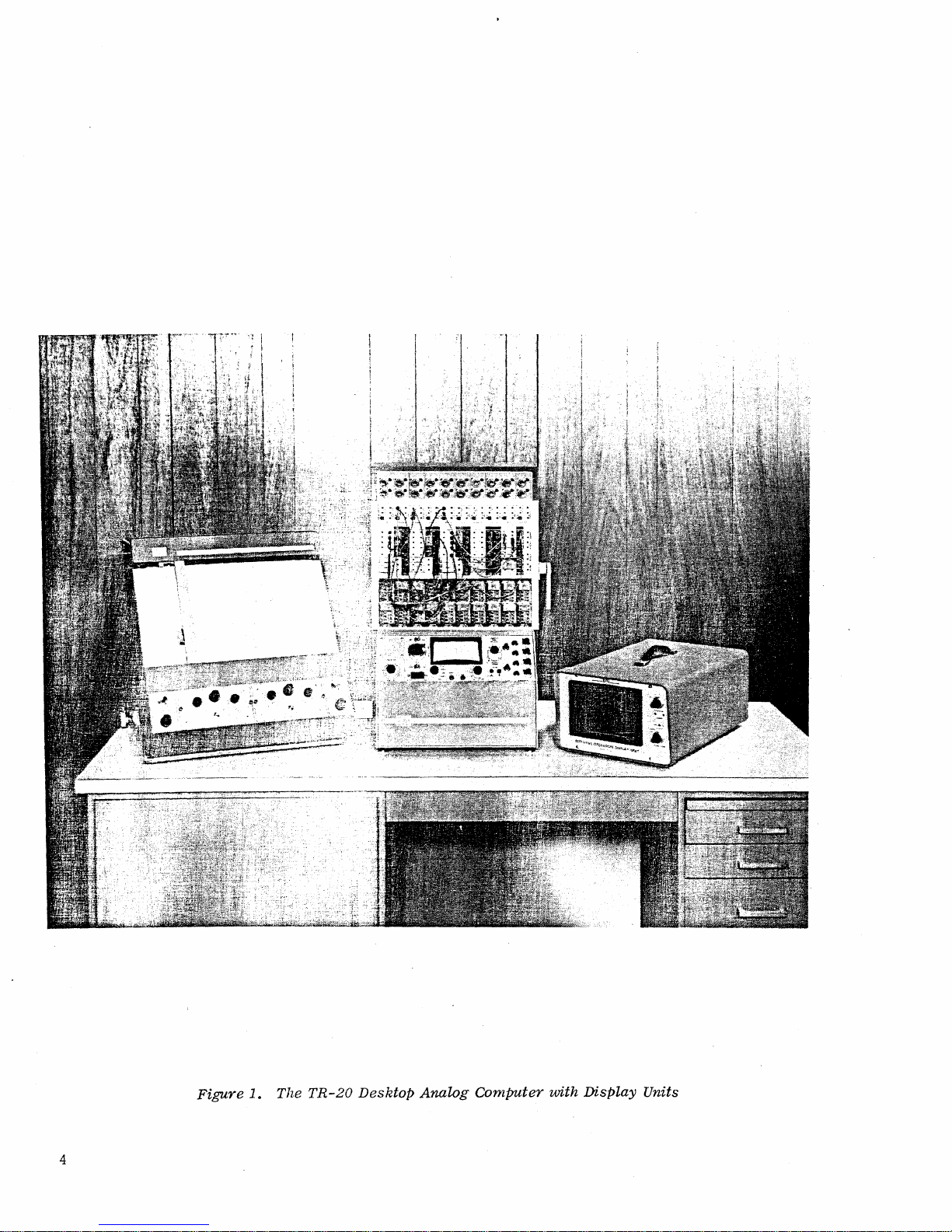
Figure
4
1.
The
TR-20
Desktop
Analog
Computer
with
Display
Units
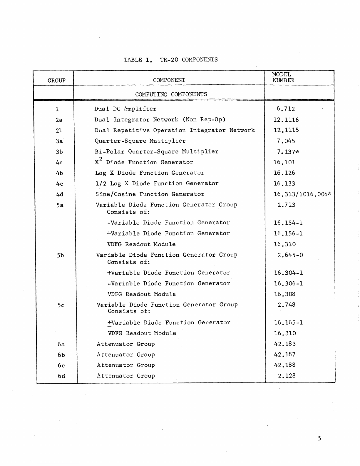
TABLE
I.
TR-20
COMPONENTS
GROUP
1
2a
2b
3a
3b
4a
4b
4c
4d
5a
COMPUTING
Dual
Dual
Dual
DC
Amplifier
Integrator
Repetitive
Quarter-Square
Bi-Po1ar
X2 Diode
Log X
1/2
Log X
Quarter-Square
Function
Diode
Diode
Sine/Cosine
Variable
Diode
Consists
-Variable
+Variab1e
VDFG
Readout
COMPONENT
Network
Operation
Multiplier
Generator
Function
Function
Function
Function
of:
Diode
Diode
Module
COMPONENTS
(Non Rep-Op)
Integrator
Multiplier
Generator
Generator
Generator
Generator
Function
Function
Generator
Generato~
Network
Group
MODEL
NUMBER
6.712
12.1116
12.1115
7.045
7.137*
16.101
16.126
16.133
16.313/1016.004*
2.713
16.154-1
16.156-1
16.310
5b
5c
6a
6b
6c
6d
Variable
Consists
+Variab1e
-Variable
VDFG
Variable
Consists
+Variab1e
VDFG
Attenuator
Attenuator
Attenuator
Attenuator
Diode
of:
Diode
Diode
Readout
Diode
of:
Diode
Readout
Group
Group
Group
Group
Function
Function
Function
Module
Function
Function
Module
Generator
Generator
Generator
Generator
Generator
Group
Group
2.645-0
16.304-1
16.306-1
16.308
2.748
I
16.165-1
16.310
42.183
42.187
42.188
2.128
5

GROUP
COMPONENT
MODEL
NUMBER
7a
7b
Tc
8a
8b
COMPUTING
Consists
Attenuator
Readout
Reference
Tiepoint
Dual
Function
Consists
Function
Readout
Relay
Comparator
Electronic
of:
Panel
Module
Network
Network
Switch
of:
Switch
Module
Comparator
COMPONENTS
Group
Assembly
(Cont)
42.
185
12.265
12.266
12.267
2.127
20.366
12.264
6.143
40.538
9
10
11
12
POWER
Regulated
Reference
Dual
DC
OPTIONAL
Repetitive
Consists
High
Repetitive
Dual
AND
REFERENCE
Power
Supply
Regulator
Amplifier
COMPONENTS
Operation
of:
Speed
Repetitive
Operation
Repetitive
SUPPLIES
AND
ACCESSORY
Expansion
Operation
Timing
Operation
EQUIPMENT
Group
Control
Unit
Integrator
Panel
Networks
10.179
43.037
6.282
2.246
20.532
36.082
12.1115
6

GROUP
COMPONENT
MODEL
NUMBER
13
14
15
16
17
18
19
20
21
22
OPTIONAL
Display
Reactor
Transport
Audio
S
Patching
Service
AC
Pre-Patch
Rep-Op
lave
Power
Overload
Cable
COMPONENTS
Unit**
Kinetics
Delay
Kit
Shelf
Cable
Panel
Slave
Panel
AND
Group
Simulator
Alarm
AUXILIARY
ACCESSORY
EQUIPMENT
EQUIPMENT
12.987
2.475*
2.448*
13.017
510.038
100.007
51.039
51.040
5
..
235
20.567
The
operator
use
the
*These
**This
1
2
computer·.
Components
Component
VARIPLOTTER®
Repetitive
should
be
described
not
required
Operation
familiar
in
with
separate
if
the
Display
the
following
manuals.
Electronic
Unit
paragraphs
Comparator,
before
Model
1110*
attempting
40.538
is
provided.
to
7

a.
Insertion
of
the
Pre-Patch
Panel
Before
on
Hold
see
hand
flush
slide
To
falling
inserting
the
pre-patch
the
Figure
side
with
to
remove
forward
b.
All
operational
is
turned
prepare
the
c.
Connect
the
the
load
load
the
TR-20
RESET-HOLD-OPER
alarm
indication
pre-patch
2.
Move
of
the
the
computer.
the
left.
the
pre-patch
Feedback
on.
Bottle
amplifiers
Application
computer
Maintenance
system
the
pre-patch
panel
panel
the
patch
when
dis-engaged,
for
the
amplifiers
plugs,
of
line
Manual,
switch
will
should
are
aligned
at
pre-patch
bay.
Turn
panel,
Amplifiers
should
for
use
Power
cord
to
be
triggered
cease.
panel,
in
a
slight
panel
Gently,
the
locking
apply
and
be
connected
as
standard
to a receptacle
and
place
the
RESET
the
operator
the
same
angle
and
to
push
a
the
light
lift
provided
as
shown
the
~osition.
due
to
order
place
th~
right
pre-patch
lever
down;
pressure
the
locking
with
in
inverters
following
OFF-ON
transients;
should
as
the
it
in
until
panel
the
to
lever.
feedback
Figure
or
summers.
switch
Initially,
after
verify
computing
the
it
pre-patch
the
panel
whenever
3a,
the
to
that
patch
contacts
forward
to
provide
precautions
the
ON
position.
the
amplifier
a
few
seconds,
the
patch
components.
bay
groove;
the
right-
until
panel
keep
the
it
will
it
computer
feedback
given
over-
the
blocks
is
from
and
in
Place
over-
d.
Under
However,
found
the
amplifier
The
amplifier
this
requirement
amplifier
balance
(Figure
serve.
switch
fier
to
reads
may
be
Amplifier
normal
at
intervals
to
be
unbalanced,
may
potentiometer
4).
To
set a balance
(1)
in
the
be
balanced.
(2)
within
triggered
Balance
circumstances,
it
balance
must
is
be
balanced
is
have
satisfied
located
The
balance
Place
BAL
Vary
two
the
position.
the
or
three
during
the
is
desirable
an
adjustment
rithin
some
sort
by
while
behind
controls
control,
computer
Rotate
appropriate
divisions
the
balancing
amplifiers
to
should
tolerance,
of
feedback
the
circuit
normal
a
are
labeled
proceed
in
the
the
Amplifier
of
process.)
will
check
no
inputs
hinged
as
reset
AMPL
zero.
remain
this
be
made.
adjustment
in
order
in
which
are
applied.
cover
with
follows:
mode.
SEL
switch
Balance
(The
balanced
condition.
If
to
the
plate
the
number
Place
to
control
amplifier
the
is
necessary.
be
balanced.
amplifier
Each
below
the
the
until
overload
for
If
an
check
amplifier
the
of
the
VoltmetEr
number
the
periods
amplifier
indicates
Normally,
is
used.
Control
amplifier
Function
of
the
Vokmeter
alarm
of
has
Panel
ampli-
system
weeks.
is
that
The
a
they
8

I
l-
Figure
2.
Inserting
the
Pre-Patch
Panel
9

SJ
INPUT
FOR
SPECIAL
RESISTORS
OUTPUTS
INPUTS
Z
GAIN
GAIN
GAIN 0.1
GAIN
1[>
b.
AN
INVERTER
10
I
{
{
{
O.
PATCHING WITH
-Z
10
10
AMPLIFIER
AMPLIFIER
10
BOTTLE
PLUGS
X
y
:[>
C.
A
SUMMER
I
2
-(X
+y)
GAIN OF
0.1
GAIN
OF
d. A HIGH
Figure
10
3.
y
Z
10
A
I
-GAIN
The
6.
712
.
AMPLIFIER
Dual DC
PATCHED
Amplifier,
FOR
GAINS OF 0.1 AND I
Showing
Use
of
-O.I(X+Y+Z)-A
Bottle
Plugs

NULL POT
REFERENCE
SELECTOR
SWITCH
VOLTMETER
FUNCTION
SWITCH
VOLTMETER
ANGE SWITCH
Figure
4.
The
TR-20
Control
Panel
11

\fuen
the
flections
warm-up
fier
unbalance
intervals
e.
The
computer
of
an
overloaded
of
the
control
fier
and
22
is
serve
respectively.
located
overloaded.
The
overload
the
problem
.the
equipment
voltages
several
plus
or
problem
a
patching
time.
computer
that
are
period.
or
in
order
Overloads
is
panel.
overloaded.
the
The
in
the
alarm
operation,
by
other
other
minus
(1)
reasons
If
reference
solution.
error,
is
first
slightly
For
unusual
integrator
to
equipped
amplifier.
amplifiers
computer
rear
of
system
short-term
than
an
those
overload
An
and
turned
high,
problems
drift,
keep
the
with
The
The
lamps
Lamps 1 to
associated
may
the
cabinet;
indicates
or
the
overloads,
normally
exist
for
is
voltage
overload
should
not
on,
but
the
meter
an
deflection
overload
visual
are
20
serve
be
equipped
it
that
computing
obtainable
clearing
indicated
may
be
in
either
be
allowed
a
check
they
that
will
might
amplifier
alarm
overload
illuminated
the
with
the
with
sounds
something
components.
unless
overloads
for
other
of
these
to
of
amplifier
return
be
below
system
alarm
whenever
20
operational
plus
an
an
audible
they
from
amplifier
than
continue
to
especially
can
be
balanced
one
that
is
located
and
minus
audio
alarm
is
wrong
Usually,
are
caused
the
computer
soon
after
21
~10.00
volts,
amplifiers
over
balance
normal
sensitive
division.
indicates
their
amplifiers;
reference
overload
when
with
no
by
they
or
22,
generally
an
will
levels
at
more
the
on
the
associated
alarm
an
the
problem
harm
is
excessively
itself.
are
the
value
adversely
extended
show
after
to
ampli-
frequent
presence
left
side
ampli-
lamps
amplifiers
that
amplifier
done
However,
noticed.
of
affecting
indicates
period
de-
a
21
is
is
patching,
to
high
the
of
affect
lit,
however,
assigned
purpose
3.
READOUT
The
operating
sloping
Figure
(2)
the
problem
amplifier,
of
the
control
4.
The
Overload
solution.
may
cause
thus
alarm
FACILITIES
controls
panel
functions
of
the
causing
system.
AND
for
area
of
unassigned
However,
operator
MANUAL
the
readout
below
the
controls
an
erroneous
MODE
the
arnpiifiers
the
fact
to
overlook
CONTROLS
and
mode
computing
are:
does
that
an
problem
control
component
not
damage
one
or
overload
solution
circuits
cradles
the
more
overload
occurring
and
are
as
amplifiers
in
defeating
grouped
shown
lamps
an
the
on
in
or
are
the
12

Control
Function
Power
Mode
Voltmeter
Voltmeter
Control
NULL
Switch,
VM
POT
Jack
Amplifier
(AMPL
ON-OFF
Function
Range
and
+lO/OFF/-lO
Selector
SEL)
Switch,
Switch,
Switch,
Reference
S4
SS
Switch,
Selector
(53)
Switch,
S2
Sl
s6
Controls
power
is
Controls
Positions
Controls
POT BUS, NULL,
Selects
ranges
provided.
Used
sure
Provides
when
NULL
Selects
balancing.
application
supply
illuminated
the
are
voltmeter
sensitivity
of
0.1, 0.3,
in
conjunction
voltages
for
the
Voltmeter
or
VM
an
position
amplifier
of
of
the
computer.
when
operational
RESET,
VM,
power
operation.
AMPL,
for
1,
with
by
the
external
Function
primary
HOLD,
voltmeter.
3,
null
inputs
for
ac
The
is
applied.
mode
and
of
and
OPERATE.
Positions
BAL.
10,
and
the
voltmeter
comparison
to
Switch
output
power
voltmeter
the
computer.
Full
30
volts
to
method.
the
voltmeter
is
in
monitoring
to
are
scale
the
the
are
mea-
or
AMPL
OUT
Overload
a.
The
readout
connecting
potentiometer
The
function
The
BALposition
dc
amplifiers.
of
the
amplifier
amplifier
SEL
switch
positions
amplifiers
movement.
Jack
Indicators,
Readout
facilities
the
voltmeter
that
of
is
rotated
are
connected
21
and
respectively.
OVLD
Facilities
is
the
related
of
the
The
AMPL
to
be
until
22
are
IND
consist
to
used
Voltmeter
SEL
balanced,
to
connected
The
of
various
to
measure
controls
switch
the
meter
the
diodes
Connected
facilitates
external
Indicate
fier
a
sensitive
points
voltages
is
Function
(S6)
(Figure
reads
stabilizers
to
the
in
monitoring
an
when
voltmeter,
in
the
described
Switch
is
used
Sa).
zero.
of
stabLlizers
parallel
to
the
wiper
connecting
overload
illuminated.
computer,
by
the
null-comparison
below.
(Sl)
to
select
The
balance
Positions
the
20
operational
of
with
the
of
any
or
measuring
in
selector
and a precision
is
used
the
potentiometer
the
plus
meter
1
the
the
when
to
AMPL
amplifier
associated
switches
balancing
stabilizer
20
of
amplifiers;
and
minus
protect
SEL
sWitch;
output
equipment.
ampli-
for
ten-turn
method.
output
of
the
the
AMPL
reference
the
meter
to
the
13

STAB. OUT,
I ,
I
II
II
I
I
I
I
I
I
STAB.
OUT,
II
II
AMP.
AMP.
,+REF
,
-REF
..
#1
#2
#20
AMP.
AMP.
[JJ
---0
[TI
---:-
........
0 I
I 0 0
: IpOT BUS] 0
1201
@JJ
---0
1221
---0
NULg
FUNCTION SWITCH
~
0 I
VOLTMETER
SI
AMPL.I
R8
8.2K
50-0-50
CRI
CR2
10500
jJa
AMP. # I OUTPUT
II
AMP.
-#2
#20
II
OUTPUT
+
REF
-REF
--0
--0
--0
--.()
I
I AMPL
[IJ
rn
[Q]
[ill
[g]
AMPL
S6
S6
SELl
SEL]
I
AMPL.\
OUT
0
J2
(a)
SAL
INULL
IpOT
BUS
FUNCTION SWITCH
(
b)
AMPL POSITION
POSITION
~
I 0
10
VOLTMETER
IAMPL.I
0
SI
OJ
~
0
IBALI
-
10FFI
0
VOLTMETER
RANGE SWITCH
S2
INULLI
IpOT BUS I 0
Figure
5.
Readout
Simplified
Schematics
14
o
VOLTMETER
FUNCTION SWITCH
SI
(e)
Circuits
VM
VOLTMETER
RANGE
POSITION
10FFI
o
SWITCH
S2
50
-0-50
10500
jJ
a -
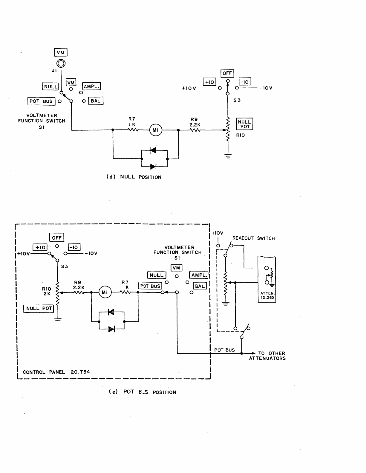
IAMPLI
o
o I
BAL
I
+IOV
10FFI
1+101
0 0
82J
-IOV
S3
VOLTMETER
FUNCTION SWITCH
SI
(d)
r--------------------------
I r:::::1
I
I
+IOV
~
RIO
2K
~
0
5QJ
O----IOV
S3
R9
2.2K
R7
IK
NULL
POSITION
VOLTMETER
FUNCTION SWITCH I r
I
NULL
I
~T
BUS
SI
IVM
I I
I 0 I
I 0 0 I
R9
2.2K
AMPL
BAL
o
I
II
II
I
I
+IOV
I
6_
INULLI
POT
RIO
READOUT
SWITCH
ATTEN.
12.265
L
________________________
CONTROL PANEL
20.734
(e)
POT
B:..s
POSITION
'------+---=----=---e-
~
i
...
TO
ATTENUATORS
OTHER

The
;21PL
in
Figure
volt=eter
range
to
the
for
AMPL
equipment-.
The
VM
position
Voltmeter
on
the
voltmeter.
The
NULL
with
in
to
side
that
respect.to
Figure
one
side
of
supplies
measured.
the
turns-counting
voltage;
null
comparison
scale.
source
source
being
has
decrease
position
Sb
where
The
o
the
OUT
Range
position
Sd.
of
the
meter.
.The
the
position
An
important
measured
no
the-
sensitivity
of
the
the
Voltmeter
voltmeter.
jack
so
of
the
switch
of
Sl
the
computer
The
voltage
the
meter.
The
reference
NULL
POT
dial
method
feature
effect
in
Voltmeter
output
that
Voltmeter
(Figure
provides
of
Range
Note
amplifier
the
switch
that
Function
Sc).
a
reference
to
be
measured
The
wiper
Reference
voltage
is
on
of
S3
of
voltage
varied
the
indicates
Selector
with
NULL
measurement
of
the
once a balance
the
measurement.
of
the
meter
Function
selected
is
the
outputs
Voltages
means
voltage.
of
the
until
POT
the
method
is
to
switch
amplifier
used
wiper
of
switch
patched
of
accurately
is
patched
the
NULL
switch
same
the
polarity
meter
indicates
polarity
is
is
that
attained.
A
large
unbalanced
establishes
to
select
the
can
be
connects
The
POT
S3
reads
the
of
accurate
no
Thus
source
provides
a
convenient
AMPL
SEL
monitored
the
into
the
measuring
circuit
to
the
VM
is
connected
is
switched
as
the
zero.
magnitude
the
unknown
to
current
the
resistance
resistance,
conditions.
the
circuit
the
input
full-scale
switch
with
VM
VM
jack
jack
is
external
to
unknown
arrangement
jack
voltage
The
to
to
of
and
the
the
to
position
the
voltage.
within
is
±p.l%
drawn
however,
shown
to
connected
the
are
read
voltages
is
shown
connected
other
position
be
of
unknown
This
of
from
of
the
the
the
full
will
The
POT
readout
comparison
depressed,
connected
position.
uator
same
is
coefficient
b.
The Mode
and
stopping
switch
relays
All
The
controls
of
computing
integrators
BUS
position
circuit
method.
+10
to
The
adjusted
Manual
Control
the
of
is
connected
When
volts
the
NULL
pot
is
bus.
POT
until
as
the
Mode
Control
switch
computer
the
operation
integrators.
components
are
controlled
Sl
is
the
connected
The
is
set
the
meter
NULL
(8S)
solutions
The
except
used
to
when
measure
pushbutton
to
the
Reference
to
the
reads
POT.
on
the
Control
and
of
of a circuit
switch
the
integrators
as
follows:
setting
the
voltage
switch
top
of
Selector
desired
zero.
Panel
establishing
which
positions
attenuators
on
associated
the
attenuator,
switch,
attenuator
The
attenuator
provides
initial
actuates
are
RESET,
are
operational
(Figure
the
pot
with
S3
must
coefficient.
a
means
conditions.
the
HOLD,
bus
an
and
is
then
reset
in
Se).
by
the
attenuator
the
wiper
be
in
the
The
set
of
starting
The
and
operate
and
OPER
all
three
The
null
is
is
+10
atten-
to
the
(operate).
modes.
IS

RESET
HOLD
OPER
4.
ATTENUATORS
One
of
the
accomplished
that
potentiometers
here.
groups
is
less
Four
use
simplest
by
using
than
are
types
ten-turn,
and
one.
often
of
attenuator
5000
most
a
useful
potentiometer
This
called
ohm
In
integrators
initial
inputs
In
are
ables
In
inputs
takes
operations
to
corresponds
attenuators.
groups
potentiometers.
the
the
removed;
are
the
place.
multiply
to
are
reset
are
conditions
to
the
hold
operate
and
attenuation
available
mode,
held
integration
performed
Both
The
mode,
integrator
integration
a
terms
groups
the
set
of
the
at
the
mode,
on
voltage
of
for
output
to
the
values
the
problem.
are
inputs
ceases
present
the
integrators
with
an
analog
by a positive
the
voltage,
are
used
use
in
are
listed
voltages
required
disconnected.
to
the
and
values.
respect
computer
therefore
interchangeably
the
TR-20,
below.
of
the
by
All
other
integrators
all
vari-
accept
to
time
is
constant
All
GROUP
42.183
42.187
42.188
2.1,28
(42.185
12.265)
The
Type
tions.
and
the
terminated
meter
module
and
The
ted
are
Quad
lower
in
&
42.183,
The
top
lower
on
available
(Type
Coefficient
end
order,
OF
NO.
Type
potentiometer
end
of
the
right
12.265)
of
each
top
to
POTS
2
2
2
4
42.187,
this
for
that
Assembly,
bottom,
potentiometer
side
patching.
mounts
potentiometer
of
on
TYPE
and
is
the
Type
the
OF
POT
Carbon
Carbon
Wirewound
Wirewound
Type
terminated
in
42.188
patching
The
Type
the
is
non-linear
42.185
is
grounded.
patchirg
Uncalibrated
Un
c-a 1 i
Calibrated
Calibrated
Groups
on
the
grounded.
module
2.128
that
mounts
module.
DIAL
brated
have
left
The
and
Group
row
of
in
The
potentiometers
similar
side
lower
both
consists
computing
the
Does
Switches
Has
Has
Has
Pots
trol
patching
of
the
potentiometer
ends
of
of a patching
control
REMARKS
not
have
Readout
Readout
Readout
located
Panel
patching
the
components,
are
potentio-
panel
termina-
area
termina-
area.
Readout
Switches
Switches
Switches
in
Con-
module
is
16

When
an
output
the
mechanical
attenuator
the
wiper
are
not
the
wiper
it
is
wiper
input
voltage
shaft.
equal.
is
more
voltage
voltage
Eo
ratio
could
convenient
be
Normally,
The
loaded
and
E.
In
is
K
times
of
set
most
by
the
to
adjusting
is
Rl
:RT is
to
the
common
amplifier
set
applied
Ein,
exact
however,
use
the
attenuator
the
wiper
to
where
the
ratio
the
of
input
an
K =
same
attenuator
the
until
attenuator
R
l/~.
as
the
electrical
by
means
attenuator
resistor.
under
the
loaded
desired
If
of
is
as
shown
the
the
loaded
is
to
In
order
conditions
output
in
attenuator
ratio
vernier
and
feed
to
is
Figure
E
o
dial
the
an
amplifier;
account
by
obtained.
6,
the
is
unloaded,
:E.
and
In
attached
two
ratios
for
monitoring
the
to
thus
loading,
the
Figure
under
switch
panel,
the
on
The
Figure
potentiometer
Note
to
the
end
The
of
itate
two
is
The
5.
7a
load.
connects
and
pot
bus,
the
control
ungrounded
7b.
that
both
ends
low
end
if
so
Type
each
attenuator
readout
potentiometer
placed
high
THE
OPERATIONAL
shows
A
applies
can
Depressing
the
of
of
desired.
42.183
within
and/or
the
circuit
pushbutton
the
wiper
+10
be
measured
panel.
attenuators
and
connects
lower
under
end
the
attenuator.
the
ungrounded
Attenuator
is
loaded
types.
the
low
end
AMPLIFIER
volts
the
of
brought
circle;
of
used
switch
to
the
to
the
by
the
are
connected
pushbutton
the
loaded
the
attenuator
potentiometer
Group
out
conditions.
The
address
the
ungrounded
in
the
TR-20
is
located
pot
bus,
top
of
null-comparison
switch
wiper
The
patching
does
not
to
a
termination
Figure
or
coefficient
potentiometers
next
removes
the
in
the
applies
to
is
not
to
include
number
setting
to
permit
to
each
the
attenuator.
method
circuit
the
pot
grounded
block
make
has a ground
the
next
7
contains
qf
the
setting
attenuator;
voltage
configuration
+10
volts
bus
and
it
convenient
pushbutton
to
schematics
potentiometer
(K)
is
is
also
applied
The
by
using
for
measuring
voltages
the
written
indicated.
grounded
depressing
wiper
the
to
the
termination
to
ground
switches.
attenuator
and
(i.e.,
near
attenuators
at
the
voltage,
NULL
shown
top
of
purposes.
may
to
symbols
the
patch
POT
in
the
be
near
the
The
facil-
1
symbol.
the
on
patched
low
wiper
for
or
2)
a.
General
When a
to
an
unit
by a constant,
ing,extracting
high-gain
perform
operational
in
the
mathematical
Considerations
dc
amplifier.
analog
integration,
square
amplifier
computer.
root,
is
operations,
The
operational
It
and
generating
used
can
used
in
the
be
in
conjunction
resulting
amplifier
used
conjunction
logarithmic
for
with
system
is
inversion,
with
functions,
input
is
the
special
and
generally
basic
summation,
and
networks
etc.
feedback
referred
most
multiplication
for
networks
to
versatile
squar-
17
as

e
in
=
Ke
in
TO
SWITCHES
ALL
+IOV---O
ATTENUATOR
GROUPS
OF
Figure
r--
I I
I
I I
L--=----i
~.~--------~--------------------------~----~~~
(0)
ATTENUATORS,
6.
An
Atterl1lator
+IOV
::~
ATTEN.42.188
~
t-----+---J
POT
BUS
SIMPLIFIED
L---
SCHEMATIC
,
!
J
TO
CIRCUITS
READOUT
~-'--
R,
T
K
Ein
--0-
(b)
GROUNDED
Figure
18
RI
RT
Ein
=
KE
KEin
7. Sche-matics
in
and
Symbols
x
T
RT
L
Y
X
Y
(C)
for
Attenuators
HI
RI
LO T
UNGROUNDED
K
(X-Y)
K(X-Y)+Y
+Y

Recall
Figure
(lb)
order
by
of
that
8):
(1)
the
(2)
(3)
3 X
the
The
gain
The
Thg
la'
amplifier
amplifier
of
the
input
open
at
dc).
is
output
amplifier:
stage
loop
gain
designed
of
-the
of
(eo)
eo
= -Ae
amplifier
the
to
have
is
related
b
amplifier
three
draws
is
essential
to
the
negligible
extremely
characteristics
summing
current:
high:
junction
A»l
voltage
ib~
(on
(see
0
the
Therefore,
equation:
Equation
ational
solely
Using
amp1i=~:2r:
depenc~~=
Equatio~
the -various
When
the
the
amplifier
opposite
norma
11y
the
amplifier
2-1
'::'::lustrates
2-1
u:s.:2:.:S
same
~(C".2.1ue
":::'utput
in
p~~rity.
100,
C-
:\:1 ohms (lOOK),
on
of
e =
(
o
the
input-output
the
as
the
the
resis
voltage
In
e
o
output
Zf
--
Zinl
one
ratio
basis
opera
tor
the
)
voltage
e
is
in
of
the
most
relationship
of
the
feedback
of
discussion,
tiona 1 amplifier.
is
used
has
TR-20
there
e.
ln
the
for
same
the
fore:
both
value
lOOK
lOOK
related
important
to
the
the
amplitude
of
e
in
to
the
characteristics
of
the
operational
the
input
following
feedb9ck
as
the
Rf and
e.
ln
R.
ln
input
voltage
CEQ.
impedance.
sub-paragraphs
and
the
input
used
voltage
for
by
2-1)
of
the
amplifier
input
the
the
oper-
is
describe
impedance,
but
is
inverter
is
Thus a +10
have a gain
on
the
.£.
A
change
examp
1e,
vo=-::..-
0=
accurac
input
~inus
of
the
Mu1tip_---------=--cation
in
th':::::~
wi
th
ratio
~
equal
e
results
one.
ratio
by a Constant
of
to
o
The
the
lOOK
lOOK
10K
in a -10
accuracy
Rf/R
..
ln
resistors
and
e.
ln
R.
ln
volt
of
results
equal
10e.
ln
output,
the
to
and
output
in
10K,
to
multiplication
the
the
amplifier
input
amplifier
is
ratio
depends
by a constant.
output
said
is:
to
solely
For
19

Figuye
20
8.
Operational
Amplifier,
Simplified
Block
Diagram

An
input
amplifier
by
using
of
plus
has a gain
a 10K
feedback
one
volt
of
results
ten.
resistor
The
multiplying
with
in
an
a
output
lOOK
of
constant
input
minus
resistor.
ten
can
volts.
be
made
This
smaller
operational
than
one
An
input
~.
When
multiple
lationship
The
circuit
more,
~.
When
the
amplifier
ance
l/pC
Equation
of
minus
Surrnnation
is
can
each
input
Integration
feedback
becomes
and
2-1,
e
o
ten
input
resistors
extended
be
used
may
element
an
Z.
is a resistor,
~n
becomes:
10K
lOOK
volts
to:
to
be
multiplied
with
Respect
integrator.
e.
~n
produces
are
used
algebraically
to
Zf
is a capacitor
If
the
an
by
Time
Zf
-0.
le
output
with
an
is
Easic
.
~n
a
feedback
sum
an
arbitrary
rather
a
capacitor
operational
of
plus
one
resistor
indefinite
constant.
than a resistor,
having
amplifier
volt.
number
an
Rf,
the
of
inputs;
the
operational
relationship,
basic
re-
further-
operational
imped-
An
indefinite
sum
of
f.
As
previously
scribed
and
parallel
formance
general
impedance
linear;
amplifier
non-linear
the
input
Other
above.
is
still
case
of
therefore,
can
operations
e
--
o
number
of
voltages.
Mathematical
indicated,
Complicated
RC
networks
governed
where
Zf
three-terminal
and
Z.
al~gst
also
be
inputs
must
used
of
E.
~n
pRC
Operations
the
operational
transfer
for
the
by
the
be
any
non-linear
in
conjunction
limiting,
1 t
-
RC
may
feedback
basic
networks
used.
e.
~n
So
be
applied
amplifier
functions
relationship
The
characteristics
dead-zone
dt
to
and
input
are
input
with
generation,
produce
has
can
be
used,
and
diodes
the
uses
simulated
impedance.
of
Equation
the
short-circuit
feedback
can
and
resistors
X2,
time-integral
other
by
than
using
The
2-1.
elements
be
approximated.
Log X,
those
circuit
For
transfer
need
to
simulate
etc.
of
series
per-
the
not
the
de-
be
The
the
21

£.
Patching
the
~3plifier
as a Summer/Inverter
Five
fier
each,
a
each
precision
section
and
value
resistor
(summing
at a point
five
To
plug
1
verter
0
patch
as
input
inputs
and
the
lower
The
one
gain-of-one
h.
The
amplifier
to
an
integrator
TR-20.
to
form
equipped
repetitive
works
are
terminals
(Figure
as
of
are
designated
of
10K
is
junction)
designated
an
amplifier
shown
terminals
amplifier
Patching
Each
two
in
shown
amplifier
network
integrators.
for
repetitive
operation
similar,
input/£eedback
the
pEtch
each,
3b).
becomes
are
connected
on
the
B
in
the
as
the
upper
is
multiplied
If
in
Figure
is
acting
of
input
the
network.
and
Amplifier
an
contains
expansion
and
(base),
red
two
Figure
operation.
are
resistors
block.
1
on
connected
to
patch
area
a summer
amplifier
inputs
3c,
as
three
integrator
Two
The
~escribed
Three
the
patch
a common
block.
and
of
or
by
the
output
a summer.
3a
is
gain-of-one-tenth
as
types
the
Model
group
to
terminals
bus,
the
the
inverter,
of
-1,
(for
patched
an
Integrator
by
of
passive
12.1116
The
(see
here.
are
terminated
of
these
block.
and
The
output
patch
Figure
and
the
example x and
of
with
providing
integrator
elements
Model
Section
The
designated
input
of
block.
insert
3a.
amplifier
the
is
supplied
12.1115
resistors
terminated
of
amplifier
two
the
at
the
two
remaining
the
amplifier
the
amplifier
a
double
A
voltage
is
y)
are
is
prong
inputs~
proper
networks
and
11
of
as
control
with
is
supplied
this
front
have a value
10.
at a point
applied
referred
connected
equal
bottle
shown
patching
are
computers
chapter).
of
resistors,
The
other
is
is
connectd
(four-prong)
to
to
plugs
in
connections
available
circuits
as a part
each
designated
terminated
to
to
-(x + y),
Figure
that
ampli-
of
lOOK
with
end
to
bottle
one
of
as
an
the
to
provide
3d.
for
necessary
are
of
Both
net-
of
SJ
the
in1
the
not
the
(1)
the
patching
straight-forward,
SJ,
0,
and B terminals
patching
the
heavy
(Figure
plugs
The
half
sections
relays
inputs
condition
tacts
fier,
age
of
the
22
connections
lines
9).
in
this
diagram
of a dual
of
are
at
the
voltage
of
K2. The
between
which
may
integrator
at
the
shown
Integrator
required
with
in
the
These
connections
area.
the
right
integrator
network,
de-energized,
SJ
terminal
is
capacitor
the
Band
have
been
remains
Network
to
convert
the
S4,
respectively
are
required
lower
side
network.
although
are
also
connected
°
terminals.
applied
constant.
12.1116.
an
amplifier
0,
and B terminals
of
on
the
cross-hatched
may
be
of
Figure
The
only
as
they
connected
to
remains
connected
during
an
12.1116
easily
9 shows
relays
one
exist
to
ground
This
the
Figure
into
integrator
area
set
ground
of
made
the
(Kl
of
in
the
(through
as
allows
operate
9
is a diagram
an
integrator.
of
the
amplifier
network.
Integrator
the
integrator
by
inserting
essential
and
K2)
contacts
hold
by
the
the
or
mode.
the
contacts
a 10K
feedback
capacitor
reset
which
Two
Network,
two-prong
components
are
common
is
shown
In
resistor)
element
to
modes,
illustrates
The
patching
connected
additional
indicated
patch
this
of
retain
for
Kl.
of
and
block
to
each.
mode,
by
the
bottle
of
one
both
The
the
the
any
output
is
to
the
by
Both
the
initial
con-
ampli-
volt-

PART
OF
6.712
DC
AMPLIFIER
XI
XlO
INTEGRATOR
INPUTS
TO
SOURCE
OF
INITIAL
CONDITION
VOLTAGE
INTEGRATOR
OUTPUTS
INTEGRATOR
OUTPUTS
'------------
SJ
IC
B
PART OF 12.1116 INTEGRATOR
10K
DUAL
INT
NET
12.1116
FROM
FROM OPERATE
KI
RESET
NETWORK
10K
10 MFD
I
I
I
I
-I
I
I
K2
BUS J
BUS
INTERNAL
CONNECTION
Figure
9.
Patching
an
Amplifier
Schematic
of
an
as
an
Integrator,
Integrator
Network
Showing
Simplified
23

When
bus.
and
its
IC
terminal
fier.
amplifier
with
always
the
hold
are
established.
the
If
The
a
computer
the
contact
to
time
be
left
or
indicated
moves
to
be
feedback
perform
lag
of
in
operate
is
placed
patching
to
the
coupled
through
capacitor
as a unity-gain
approximately
the
reset
modes,
in
alternate
is
mode
to
assure
the
reset
connection
a
10K
now
shunted
inverter
0.5
seconds.
for
at
that
mode,
in
position
input
least
the
relay
the
RS
shown.
resistor
by a 10K
(for
For
the
this
one-half
correct
voltage
area
This
to
resistor.
initial
reason,
second
initial
is
the
is
present
made,
allows
base
This
condition
the
before
condition
K2
is
a
voltage
of
the
allows
computer
switching
on
the
energized,
at
ampli-
the
voltage)
should
potentials
reset
the
to
When
This
the
path
The
ard
example,
the
applies
amplifier.
for
patching
operation.
reset
mode;
reset.
condition
computer
the
if
This
for
situations
(2)
viously
values
described
(10
illustrates
Note
a
network
in
The
that
12.1116
the
Operate
the
Network.
in
standard
balanced-armature
between
operate
operation.
or
repetitive
grator
scribed
has a feedback
in
the
input
Since
amplifier,
connections
For
the
RS
remaining
allows
the
is
provided
Integrator
mfd
and
the
patching
patching
the
cross-hatched
rep-op
and
Reset
and
Relay
operation.
the
appendix.
is
switched
potentials
K2
and
special
connection
in
the
value
next
solution.
in
Network
principally
0.02
mfd)
connections
An
additional
mode.
relays
relay
(K3
reset
Kl
selects
capacitance
to
is
de-energized,
integration
in
the
situations,
is
hold
when
reached
the
appendix.
by
allow
connection
area
(Kl
of
Figure
modes
the
If
the
the
operate
at
the
SJ
with
cross-hatched
these
deleted,
the
other
during
Patching
12.1115.
providing
a
500
and
the
to
the
patching
designated
and
K2
of
10).
very
rapidly,
correct
value
connection
of
10
mfd
mode,
terminal
the
capacitor
respect
area
connections
the
integrator
integrators
a
solution
and a brief
This
two
network
values
to 1 change
circuit
amplifier
connection
SPEC,
Figure
This
in
for
9)
allows
a
necessary
of
feedback
the
either
K2
de-energizes
of
the
provides
to
time
have
been
may
cannot
in
to
description
differs
of
feedback
in
time
arrangement
are
identical
is
required
if
the
have
the
SPEC
area
mode.
network
the
takes
indicated
be
different.
be
the
computer
be
used
from
scale.
of
integrator
been
replaced
integrator
requirement
capacitance
is
delected,
T~is
and
Kl
to
the
only
place.
for
placed
as
an
of
these
th~
network
capacitor.
Figure
the
network.
to
those
on
the
is
to
by a single
to
for
for
patching
energizes.
base
feedback
.
stand-
For
in
the
are
being
initial
spe~ial
These
10
for
integrator
be
used
be
switched
repetitive
normal
the
inte-
is
de-
of
pre-
Relay
gized
K2
Operation
equipped
RESET
K2
during
is
energized,
position
grounds
the
relay
with
the
and
the
operate
the
(K3).
12.1115
the
SJ
input
and
SJ
input
Therefore,
Networks,
COMPUTE
rep-op
position.
24
during
the
reset
modes,
is
connected
when a problem
the
Mode
TIME MILLISEC
and
through
to
the
Control
switch
hold
CRl
operate
is
being
must
modes.
or
switch
CR2
contact
set
must
be
placed·
The
relay
respectively.
of
the
up
on a computer
be
placed
in
the
is
ener-
When
Repetitive
in
the
OFF

SJ
B
SJ
10
TO
SOURCE
CONDITION
OF
INITIAL
VOLTAGE
DUAL
NET
J--~--
INT
12.1115
50K
____
RESET
l A-o---if---
+---+..I
KI
K3
CRI
CR2
FROM
RESET BUS
FROM
OPERATE BUS
FROM
TIME
BUS
10 MFO
0.02
SCALE
........
MFD
Figure
Showing
10.
Simplified
Patching
an
Amplifier
Schematic
to a Rep-Op
of
Integrator
Integrator,
Network
25

6.
Q~~RTER-SQLARE
a.
General
The
quarter-square
duce
-Yo
the
The
a
four
In
addition
mathematical
operation
Description
quadrant
to
operations
of
the
MULTIPLIER
multiplier
product
multiplication,
quarter-square
is
used
proportional
of
division,
in
conjunction
to
the
TR-20
squaring,
multiplier
XY
from
multiplier
is
based
and
with
inputs
square
on
a
is
dc
amplifier
of
+X,
capable
root
the
-X,
of
extraction.
identity:
to
pro-
+Y,
and
performing
which
squaring
tain
erate
multiplier
multiplication
the
are
Operators
plier
The
The
square
ages
inputs
The
form
back
reduces
biased
a
segmented
squaring
summed
are
b.
Multiplication
general
DFG's
of
has
is
unit
the
element.
multiplication
operations
diode
assembly
of
cards
in
an
who
are
referred
configuration
contain
the
sum
the
proper
positive.
is
patched
input
network
The
are
performed
networks.
straight-line
contains
input
conduct
external
interested
biased
of
signals
to
the
diode
the
input
polarity.
as a multiplier
of
input
voltages
to
the
The
approximation
four
of
at
anyone
amplifier.
in
the
TR-20
of
the
Maintenance
the
networks'
voltages
A
amplifier;
operations
by
diode
diode
squaring
quarter-square
positive
either
circuit
in
are
function
plus
time.)
that
to
DFG
Figure
a
patched
of
function
generators
to a square
cards
or
The
details
Manual.
multiplier
produce
the
DFG
conducts
llb.
3550
ohm
to
summation
generators
that
are
minus
outputs
of
the
a
current
when
only
The
resistor
the
+X,
and
or
squaring
law
curve.
connected
polarities.
of
the
quarter-square
is
shown
the
sum
when
squaring
(R65)
-X,
+Y,
squaring.
(DFG's)
squaring
proportional
of
the
cards
and
so
in
the
is
that
cards
The
as
(Only
Figure
input
sum
the
-Y
The
con-
gen-
complete
to
permit
two
of
cards
multi-
lla.
to
the
volt-
of
its
(DFG's)
feed-
terminations.
The
output
reversing
must
A
be
the
input
fier
put
Division
can
resistor
programming
c.
26
voltage
the
+X
patched
voltages
be
Division
of a variable
used
is
symbol
in.
0.355
and
to
from
-X
The
should
sum
since
for
voltage
the
inputs
squaring
not
additional
the
amplifier
or
be
obtained
the
amplifier
multiplier
A
by a variable
the
cards
inputs;
is
-
~~.
+Y
and
have a variable
from
has a 3550
is
shown
The
-Y
potentiometers.
the
gain
voltage
output
inputs.
for
in
Figure
ohm
B
is
All
input
an
additional
feedback
llc.
is
accomplished
changed
four
input
impedance,
The
resistor.
to
output
10K
+
~~
voltages
therefore
ampli-
ohm
by
placing
by
in-

+Xo
-X
J
r---
~
DFG
+IN
DFG
+IN
>-
+xo
-X~
+x
-x
So
+YO
-Y
J
°0
MULT
7.045
o.
SIMPLIFIED
--1
DFG
-IN
DIAGRAM
+X
-X
+y
OF
-X
+X
DFG>
-IN
3550
UNIT
R65
-y
0
.~
>
S
So
+Y
O
-Y~
°0
MULT
7.045
8.
:b.
MULTIPLIER
0
8~0
V
+y
-y
PATCHING
-xv
10
-xv
10
-y
Figurf!
11.
Quarter-Square
c.
SYMBOL
Multiplier
Patching
27

the
multiplier
12.
Assume
junction
is
satisfied
that
of
amplifier
in
by
automatic
the
the
feedback
output
1,
CB
+ A
10
voltage
the
null
o
changes
loop
of a high-gain
of
relationship
in
the
amplifier
value
1
of
amplifier
is
C;
C.
Therefore:
then
as
at
shown
the
in
Figure
summing
Note
voltage
in
its
at
the
The
following
that
place
although
B
must
output
C
the
always
(by
interchanging
C
of
amplifier
restrictions
(~)
The
to
output
(~)
The
this
requires
by
other
lOA
--
B
voltage
be
positive.
+
lOA
B
absolute
the
absolute
amplifiers.
divisor
implies
negative
polarity
1.
must
B
that
A
can
have
If
the
inputs
be
placed
value
value
must
an
indeterminate
the
high-gain
feedback,
of
the
B
of
not
both
is
always
to
+Y
on
the
divisor
of
the
change
and
this
voltage
positive
and
the
division
dividend
sign.
or
amplifier
can
B.
and
negative,
-Y)
will
B
must
A
It
infinite
(amplifier
only
negative
then
produce
circuit:
be
greater
to
avoid
must
quotient.
be
arranged
not
values,
the
use
than
overloads
go
to
The
1)
be
for
the
of
-B
or
equal
in
the
zero,
surrounded
one
for
circuit
or
the
Circuits
7.
The X2 Diode
duce
inpu t vo 1 tage.
The X2 DFG
accepts
networks
x
a.
2
an
using
DIODE
General
output
contains
positive
similar
the
quarter-square
FUNCTION
Description
Function
voltage
two
input
to
those
GENERATOR
Generator
that
voltages;
is
independent
in
28
multiplier
is
used
proportional
one
the
quarter-square
in
sections
accepts
are
summarized
conjunction
to
the
square
that
negative
generate
multiplier
in
with a dc
or
square
quadratic
input
voltages.
are
the
appendix.
amplifier
used
root
of
curves.
Biased
to
approximate
to
the
pro-
One
diode

the
X2
portional
DFG
in
b.
A
simplified
the
upper
DFG
accepts
the
DFG
can
be
A
typical
yield
put
element
must
be
input
obtained
inputs.
function
to
the
the
feedback
Generating
diagram
portion
only
output
used
wherever
use
two
independent
of
negative;
impedance,
from
by a series
square
root
loop
the
Square
of
of
the
positive
is
zero.
required.
of
the
unit
squaring
an
amplifier
the
voltage
the
voltages
potentiometers.
of
of
an
the
X2
patching
inputs.
Resistor
is
that
straight-line
of
an
input
amplifier.
of
an
DFG
is
block
If
Rf (R52)
illustrated
circuits.
has a 3550
Y
must
applied
The
output
Input
shown
the
be
to
segments.
voltage
Voltage
in
accepts
input
is
in
Figure
In
each
ohm
positive.
the
-IN
amplifiers
is
Figure
only
voltage
not
feedback
and
An
obtained
(Single
l3a.
negative
has
associated
l3b.
case,
the
Since
+IN
can
output
by
placing
Polarity)
The
DFG
inputs;
the
wrong
with
The
unit
DFG
is
resistor.
the
DFG's
terminations
be
used
voltage
pro-
the
terminated
the
lower
polarity,
either
is
used
The
DFG;
patched
as
voltage
the
have a variable
should
to
sum
additional
X2
not
on
it
to
in-
X
be
A
programming
c.
2 X2
X
DFG's
The
voltage
duces
X
of
fier
Thus
an
is a positive
amplifier,
1.
for
Circuits
8.
LOG X DFG
a.
The
Log X
voltage
base
DFG's
or
is
rithmic
duced
as
by
voltage
symbol
Generating
are
X
where
output
2.
This
an
signal
input
using
AND
General
DFG's
that
is
natural
in
the
curve
for
summing
sensitive
for
the
the
Square
connected
-10 ~ X ~ +10.
of
+X2/l0
voltage,
This
of
the
X2
1/2
is
either
from
the
output
inverted
DFG
are
LOG X DFG
Description
are
used
in
proportional
logarithms
form
of
straight-line
a
single
the
outputs
switches
2
X
DFG
of
an
as
shown
When X is
amplifier
lower
is
applied
and
polarity,
summarized
conjunction
to
the
and
antilogarithms
polarity
of
simple
..
is
sho"m
Input
in
Figure
DFG
conducts
appears
the
with
logarithm
segments
input
limiter
Voltage
negative,
1;
the
through
output
in
the
voltage.
in
Figure
14
lower
and
resistor
at
appendix.
a
dc
of
can
that
circuits
(Bi-Polar)
to
generate
the
generates
the
output
of
amplifier
amplifier
the
be
closely
The
l3c.
upper
DFG
does
Rf to
of
input
signal
generated.
desired
that
+
10
from
DFG
conducts
not
conduct.
_X2/l0
the
base
amplifier
1
is
+X2/l0.
to
produce
voltage.
The
approximate
function
use
solid-state
an
at
the
of
1
an
output
a
input
and
ampli-
as
output
loga-
is
pro-
When
output
+X2/lO.
Common
of
the
pro-
diodes
The
Dual
Log
X DFG,
generators.
negative
input
voltage,
One
output
generator
voltage
-X,
and
Model
16.126,
accepts
Y =
-5
produces
consists
a
positive
loglOlOX.
a
positive
of
two
input
The
output
independent
other
voltage
voltage,
generator
X,
Y =
logarithmic
and
produces
accepts
+5
10glO
function
a
negative
IlOXI.
a
29

+A
0
+ y
+B
x
-B
+
S
B
0 0
-lOS
IBI>
0<
+IOA
AS
B S
B
+10
+10
I A I
-lOA
-
B
Figure
-INa
So
°0;
X2DF~
1---1
-INPUTS
R51
J\
A A
3550
R~
+INO
So
°0
2
x
16.101
DFG
2
x
DF~;>--
...--t
+INPUTS
R53
AAA
vv"
3550
~
R5
~
35
2
50
12.
Division
-IN
X
+IN
y
X2
Circuit
5
0
for a Quarter-Square
R~
5
0
DFG
16.101
Multiplier
X
-IN
+IN
y
X
DFG
+X2
10
X
DFG
_y2
10
2
2
-IOV
S X S °
+IOV~y~O
10
_y2
10
Q.
SIMPLIFIED
30
OF
DIAGRAM
UNIT
b.
Figure
TYPICAL
13.
r DFG
PATCHIN G
Patching
c.
SYMBOLS

0
X
-IN
i-IN
2
X
OFG
X2
OFG
S
Rf
3550
S
0
B
0
B
0
+X2
10
Figure
14.
Generating
+T
10
for
-10
< X <
--
+1
0
31.
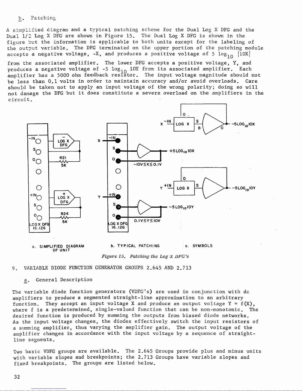
b.
Pstching
A
sirnpl~£ied
Dual
figure
the
accepts
1/2
~ut
output
a
Log X DFG
negative
diagram
the
information
variable.
and a typical
are
shown
is
The
DFG
voltage,
in
Figure
applicable
terminated
-X,
and
patching
15.
produces
to
on
scheme
The
Dual
both
the
upper
a
positive
for
units
the
Log X
except
portion
voltage
Dual
DFG
Log
X
is
shown
for
the
of
the
patching
of 5 10glO
DFG
and
in
the
labeling
the
of
module
IIOXI
from
the
produces
amplifier
be
less
should
not
damage
circuit.
associated
a
negative
has a 5000
than
be
taken
the
-IN
O
So
00
0
0
+INO
So
0
0
LOGX
OF
16.126
0.1
volts
not
DFG
R21
5K
lOG
DFG
R24
amplifier.
voltage
ohm
to
but
+
X
5K
feedback
in
order
apply
it
does
of
-5
an
constitute
X
Y
The
lower
10glO
res~stor.
to
maintain
input
-IN
S
lOY
voltage
0
0
0
+IN
S
0
OG
X
DFG
16.126
DFG
from
The
accuracy
a
severe
accepts
its
input
of
the
X
~
...... -
")0..
............
a
positive
associated
voltage
and/or
wrong
overload
-IN
+5
lOG 10 lOX
-5l0G1010Y
voltage,
amplifier.
magnitude
avoid
polarity;
on
the
should
overloads.
doing
amplifiers
-5l0G1010X
Y,
and
Each
so
not
Care
will
in
the
o.
SIMPLIFIED
9.
VARIABLE
a.
The
variable
amplifiers
function.
DIODE
General
to
They
where f is a predetermined,
desired
As
the
a summing
amplifier
line
Two
with
fixed
function
input
amplifier,
changes
segments.
basic
VDFG
variable
breakpoints.
DIAGRAM
UNIT
OF
FUNCTION
GENERATOR
Description
diode
function
generators
produce a segmented
accept
an
input
single-valued
is
voltage
groups
slopes
produced
changes,
thus
in
accordance
are
and
The
by
varying
available.
breakpoints;
groups
32
b.
Figure
straight-line
voltage
summing
the
diodes
the
with
are
TY P ICAl
15.
Patching
GROUPS
(VDFG's)
amplifier
the
The
the
listed
PATCH I
the
2.645
X
and
produce
function
the
outputs
effectively
input
2.645
2.713
below.
NG
Log
X JJFG's
AND
2.713
are
used
approximation
an
that
can
from
switch
gain.
voltage
Groups
Groups
The
by a sequence
provide
have
C.
SYMBOLS
in
conjunction
to
output
be
biased
the
output
variable
with
an
arbitrary
voltage
Y =
non-monotonic.
diode
input
plus
networks.
resistors
voltage
of
and
of
straight-
minus
slopes
dc
f(X),
The
of
the
units
and

GROUP
NUMBER
+VDFG
UNIT
READOUT
MODULE
-VDFG
UNIT
2.713-0
2.713-1
2.713-2
2.645-0
2.645-1
2.645-2
16.156-1
16.156-1
---
16.304-1
16.304-1
---
16.310
16.310
16.310
16.308
16.308
16.308
16.154-1
-
--
16.154-1
16.306-1
---
16.306-1
15
,t$
READOUT
VDFG
MODULES
UNITS
NOTE:
The
J-63,
16.165-1
or
Figure
J-64:-
16.
+VDFG
VDFG
Unit
Mounting
may
be
Locations
located
in
J-61,
J-62,
33

The
16.154
and
reference
identical
(fixed
units
b.
Minus
except
breakpoint)
described
Setup
VDFG
polarities
for
diode
VDFG
in
this
Procedure
Unit
are
and
section.
(Fixed
is
identical
reversed.
and
reference
the
Breakpoint
16.304
to
the
Similarly,
polarities.
Plus
(variable
VDFG's)
16.156
the
Plus
VDFG,
16.306
and
Therefore,
breakpoint)
except
16.304
the
16.156
VDFG
that
are
Units
Plus
the
diode
are
only
simplified
A
shown
the
The
a
sired
in
input
function
fixed
at
+4, +5,
tray
forward,
Figure
disconnect
Adjust
+2.6
pot
volts.
to
output
diagram
Figure
voltage
shown
breakpoint
(I)
Prepare
the
output
+6,
+7,
(2)
Open
exposing
l8c.
(3)
Turn
the
the
PARALLAX
(4)
Re-connect
provide
voltage
17.
polarity
in
VDFG.
+8,
the
the
output
an
input
is
reached
and a typical
This
information
restrictions
Figure
l8a
Proceed
a
of
+9,
door
pot
table
the
and
the
VDFG
of
to
(Figure
VDFG
+10
below
adjustment
potentiometers
amplifier
obtain
amplifier
of
+1
(+3.3
when
volts.
the
volt.
volts
patching
is
used
as
follows:
l8b)
the
control
1
from
the
1
to
Adjust
scheme
is
applicable
for
each
to
of
input
unit
illustrate
the
appropriately
voltage
panel
potentiometers.
fully
the
counter-clockwise.
VDFG,
appropriate
the
+IN
terminal,
the
+1
in
this
case).
for
to
must
and
slide
and
output
volt
the
the
the
is
equal
Patch
ground
voltage,
and
pot
16.156
other
be
Plus
VDFG's,
observed.
procedure
scaled
to
the
appropriate
the
circuit
the
in
adjust
until
the
VDFG
however,
for
setting
voltages
0,
+1, +2,
shown
Temporarily
+IN
terminal.
this
case
the
setup
correct
is
up
de-
+3,
VDFG
in
(5)
output
voltage
(6)
correct
output
potentiometers.
volts
(O
to
(7)
function
close
£.
variable
The
from 0
adds
but
setup
sample
procedure
function
steps
i~
the
cover.
Setup
to
+10
considerably
requires
information,
function
for
to
required.
Apply
is
attained.
Continue
voltage
The
-10
volts
Check
well
adjusted.
Procedure
breakpoint
volts
improved
a more
selected
setting
become
an
input
to
change
for
slope
the
adjustments
for
a Minus VDFG).
complete
(Variable
VDFG's
(Model
16.304),
complicated
and
includes
is
a
function.
familiar
of
+2
volts.
For
the
the
each
input
setup
Slide
the
Breakpoint
provide
flexibility
setup
a
procedure
complex,
with
the
Adjust
sample
input
voltages
increment
must
(preferably
VDFG
for
tray
ten
or 0 to
and
accuracy
procedure.
and
is
It
is
suggested
characteristics
the
function
by
be
made
with a plotter)
into
VDFG's)
variable
-10
volts
for
the
intended
+2
volt
shown,
sequentially,
adjusting
in
order,
its
operating
breakpoints
(Model
over
This
setup
that
the
sub-paragraph
of a sample
to
illustrate
the
of
the
pot
until
this
value
and
the
appropriate
going
16.306).
fixed
operator
VDFG
and
the
is
obtain
from 0 to
to
ensure
position
in
the
This
breakpoint
provides
function.
the
step-by-step
set
the
correct
+4.0
the
that
and
interval
feature
up
this
setup
volts.
slope
+10
the
VDFG's,
general
The
34

-
B2?l
3550
r----r---l
:::~~
- .
0
+v OFG
2
0
16.310
1-
~IOK
~
__
...1
+x
I
I
L
__________
O.
SIMPLIFIED
f(x)
_
+v
16.
SCHEMATIC
+x
OFG
1~6
+IN
+
VDFG
c. PATCHING
3550
82
I----~
B
SYMBOL
o
f
(x)
02
~~------------~
+v
OFG
16.310
b. PATCHING
Figure
17.
± VDFG Patching
35

+8
+7
+6
+5
+4
+3
+2
+1
.
.
-I
-I
_
OUTPUT
-
./'
"\.
'\
V
~
/V
V
......
\
'"
\
+9
f\
+10
INPUT
INPUT
0
+1
+2
+3
+4
+5
+6
+7
+8
+9
+10
ADJUST
PARALLAX
+IV
+2V
+3V
+4V
+5V
+6V
+7V
+8V
+9V
+IOV
OUTPUT
+2.6
+3.3
+4.0
+5.0
+5.0
+5.7
+5.7
+4.6
+4.2
+3.0
+1.0
0
0
+1
-
_L..
2
+2
+3
+4
O.
SAMPLE
b.
TABLE
+5
+6
FUNCTION
OF
+7
+8
FUNCTION
VALUES
-10
----{
Figure
36
18.
'>-----f
Sample
+IN
VDFG
c. SETUP
Function
+
PATCHING
and Setup Information
B
>---~~---
OUTPUT

the
VDFG
conducting
"corner"
line
segment
"rounding"
setup
To
procedure
avoid
(1)
are
in
these
Basic
not
state
the
curve
effect
(~
(!0
(,£)
Setup
ideal
is
DFG
not
output
is
usually
slvitches.
abrupt,
improves
for
two
reasons:
It
takes a variation
voltage
breakpoint
clearly
If
the
either
interaction
sive
approximation
set
the
touch
what
lengthy.
difficulties,
The
breakpoint
microamp
the
"knee"
resistor
DFG
output.
Considerations.
The
but
graph,
the
to
switch
is
a
only
an
accuracy
complicated
defined.
breakpoints
one
of
them
necessitates
it
value
up,
then
the
at
breakpoint
following
is
of
current
of
the
of
lOOK,
This
The
transition
gradual.
rounded
corner
approximation
of
the
of
about
the
diode
by
are
close
will
affect
setting
-
first
return
to
rules
defined
as
through
diode
this
is
cha,racteristic
current
relatively
diodes
used
from
As a result,
will
to a desired
DFG.
However,
one-fifth
off
or
on.
the
fact
together,
the
value
the
set
the
value
2,
then
2,
etc.
are
the
input
the
diode.
contributes
easy
in
the
the
non-conducting
instead
result.
of a volt
Hence
that
adjusting
at
function
at
return
This
process
adopted:
voltage
This
curve.
to
measure.
construction
of a sharp
Since
smooth
it
complicates
in
the
setting
the
breakpoint
the
the
other.
values
breakpoint
to
breakpoint
can
that
produces
is
approximately
With a feedback
0.10
volt
to
the
curve
the
value
This
by
succes-
1,
be
to
the
of
the
straight-
this
the
input
of
the
is
not
at
then
1,
and
some-
1.0
on
(2)
(~
To
minimize
breakpoints,
together
striction.
quired
gether
and
If
be
points
Additional
(~
Pot
not
sistor
into a DFG,
diodes
(.1?)
Insufficient
segment
more
or a pot
ment,
volt
than
to
make a diode
than
the
interaction
the
spacing
less
severe,
will
Considerations
Loading.
from a pot.
from
conducting,
is
slope
may
the
maximum
divided
interaction
adjacent
one-fifth
Since
0.2
a
volt
change
described
is
about
and
the
be a smooth
The
DFG
The
the
pot
output
the
load
and a loading
Slope.
not
enough
is
needed,
be
placed
obtainable
by
the
pot-setting
between
breakpoints
of a volt.
of
change
will
produce
0.2
to
portion
curve
input
load
should
on
terminal
on
the
pot
The
maximum
for
all
the
DFG
in
the
the
should
about
state,
in
above
0.25
of
rather
any
pot
will
error
slope
functions
feedback
feedback
slope
(e.g.,
function
This
0.2
volt
two
effect
will
volt,
the
graph
values
never
is
be
not a serious
in
the
breakpoints
only
make
the
one
setup
interaction
between
than a straight-line.
always
should
to
depend
per
corne
from
always
ground.
will
of 1 volt
to
be
resistor
path.
segment
a
pot-sett~ng
If a pot
on
the
result.
per
generated.
can
With
is 1 volt
at
different
placed
closer
input
closer
breakpoint,
difficult.
the
break-
an
amplifier,
be a fixed
is
number
volt
be
increased,
this
arrange-
per
of
1/2
reis
to-
will
fed
of
per
If
gives
re-
re-
37

-10
+IN
+
VDFG
-10
-0---Q
O.
BREAKPOINT
I
--
SETUP
TO OUTPUT
MONITORING
CIRCUIT
PATCHING
(PREFERRED)
~+IN
~
--
-
<8
/ REMAINDER
SAME AS ABOVE
:g
O~
CIRCUIT
,
b.
BREAKPOINT
38
Figure
SETUP
PATCHING
19.
Breakpoint Setup Patching
(ALTERNATE
METHOD)

a
slope
in
slope
this
Even
effect
the
pot-setting
sent
volt
To
lOOK
find
tween
the
no
feedback
criterion
adjacent
i-th
of 2 volts
will
increase
will
sample
of
0.050
noise
problems.
should
for
out
whether
breakpoints
and
the
per
not
be
curve
setting
amplification
(i
+
f(X
i
x.
l l
volt
the
noise
objectionable
shown
(slope
When
be
used
may
l)st
+
1) -f(X
+ 1 - X.
per
segment).
level
in
Figure
of
20
volts
setting
(no
pot).
the
breakpoint
is
be
tabulated.
breakpoints
)
i
This
proportionately,
with
20c,
reasonable
which
per
volt)
breakpoints,
Otherwise
will
necessary,
is:
increase
not
the
The
gains.
requires
should
the
the
0.10
apply.
slopes
slope
but
a
pre-
standard
be-
between
(3)
Sample
(4)
and
(5)
are
the
same
modif~cations
funct~on;
tion
not
required.
opera~or
uators
quire~
used.
The
attenuators
when
settling
care~~ly
ooes
are
number
The
the
order,
for
not
to
determine
(4)
available,
method
setup
the
breakpoints.
to
of
example,
exceed
Experience
Breakpoint
of
is
assure
This
except
slope
slope.
volt
per
volt,
slope
volt.
all
Hence,
per
volt
ments
Function
used
are
the
for
also
basic
I
when
attenuators
described
are
required
complete.
maximum
is
easily
for
of
For
per
and
(The
diodes
except
does
the
volt,
no
the
as
calculated.
the
center
curve
instance,
and
amplification
slope
slope
that
are
for
long
not.)
Setup
the
setup
used
for
the
procedure
if
thesegrnent-to-segment
volt
patch
gained
to
Setup
The
per
volt,
deviate
Patching.
the
configuration
is
not
in
Figure
for
The
steps
while
setup
first
accuracy
slope
is
not
if
successive
increments
at
any
conducting
the
center
as
the
Procedure.
of
the
setup
may
be
the
setting
from
If
available,
19a
only,
part
outlined
of
the
It
(the
as
important
a
function
would
point,
slope,
change
sample
of
any
required
feedback
up
the
steps
sufficient
shown
the
is
much
and
of
the
in
diode
is
important
slope
slopes
be
are
is
at
the
in
slope
The
steps
function.
arbitrary
change
pot
the
in
circuit
faster,
are
setup
this
generated
to
at
x =
as
the
had a center
of
1.50,
necessary,
all
the
any
less
~
point,
than
of
plus
slope
between
listed
The
function.
for
the
setup
of
slope
(pot
17
of
sample
function
provided.
coefficient-setting
Figure
released
of
and
19a.
Figure
therefore
for
procedure
procedure
should
function.
realize
0),
the
increment
slope
2.10
the
and 3 volts
since
one
slopes
the
volt
the
may
exceed
successive
in
Sub-paragraphs
same
steps,
of a specific
for a given
Figure
permits
If
the
19b
other
consists
be
that
actual
in
of
0.85
center
per
due
center
1
volt
seg-
in
Some
func-
22a)
is
the
attenre-
may
be
preferred.
functions
of
followed
to
slope.
39

- SECOND
EIGHTH
NINTH
-
g
TENTH
o.
TABLE
LOCATION
ENDPOINT
Xo -LEFT
XI -FIRST
X2
X3 -THIRD
X4 -FOURTH
X5 -FIFTH
X6 -SIXTH
X7 -SEVENTH
XB X
XIOXII -RIGHT
BREAKPOI"'T
BREAKPOINT
BREAKPOINT
BREAK
PO'
BREAKPOINT
BREAKPOINT
BREAKPOINT
BREAKPOINT
BREAKPOINT
BREAKPOINT
ENDPOINT
OF
FUNCTION
NT
X
0.00
0.35
0.85
1.10
1."5
2.85
3.85
6.20
7.90
8.55
9.00
950
VALUES
!
I
!
I
fIX)
0.00
!).81
9.3"
9.93
9.36
3.67
1.69-
0.89
1.56
3.20
6.75
12.00
+0.6
b.
BREAKPOI
€I -
A.
-
NT
CURVE
ENDPOINT
BREAKPOINTS
LOCATION
+0.4
I
-0.6
I
-0.8
+10
'~~
+8
1/
Ih\
I NPUT VOLTAGE
I
+8
I
1
1
1
1
1
1
1
:
:
:
ii' f I
i :
I
T
I
I
I
I
I
I
I
I
f
f
:
: : I 1 1 I /
:
IW
f 1 I
: I
i
I :
I I
I I i
~
ill
7.90
f-/
Ci)!
:!
\ i I
~~!
\
@
\V
+9
900
~
Jf
+10
v
/
P
+2
c.
PLOT
OF
DESIRED
FUNCTION
_______
CURVE
CURVE
BEFORE
AFTER
TRIMMING
TRIMMING
Figure 20. + Variable
40
+1
INPUT VOLTAGE
+2
'-':----.....
~.-___
I ----.::
+3
+4
Breakpoint
r-=:-:::-
-
~
+5
Diode Function
I
I /
+6
-
~v
-::
+7
Generator
-
+8 +9
Sample
+10
Curves

(~
Prepare
(Figure
specified
a
table
20a).
at
of
The
twelve
values
function
points
for
(for
XU,
the
Xl'
function
a
Plus
X2,
VDFG)
•••
to
XII.
be
generated
can
Of
be
arbitrarily
these,
the ten
the
XII = +10
gether
graph
important
most
Figure
to
the
ground
the
the
Set
(~
points
the
Rotate
(~
counter-clockwise,
this
aids
Set
(~
the
internal
other
accurate
computer
16.304
all
center
manner.
the
PARALLAX
than
of
the
l8a
twelve
the
breakpoint
are
slope
in
identifying
output
two
volts.
points
points
are
endpoints.
No
0.2
volt.
function
of
delineation.
is
used,
values
low
end
in
the
Plus
position.
VDFG
close
to
pot I fully
This
(amplifier
potentiometer.
are
two
of
These
to
occur
inflection
set
the
of X specified
of
even
reset
forward.
pots
+10
Ground
and
step
the
numbered
mode,
fully
volts).
clockwise.
continue
helps
breakpoints
16)
called
We
these
values
If
attenuators
clockwise
the
prevent
approximately
breakpoints
should
points
at
locations
and
other
the
patching
and
Place
input
alternating
pick
should
in
the
pots
slide
the
to
Rotate
amplifier
during
Xo = 0,
should
be
on
areas
arrangement
(1
through
table.
2
through
the
(this
function
amplifier
slope
the
the
to
(corners)
be
selected
the
requiring
tray
means
pot 2 fully
slope
overload
setup
zero
and
and
normally
closer
from
curve
12)
Be
12.
containing
by
near
the
of
accurately
sure
Place
all
break-
switch
14.
pots
and
procedure.
adjusting
to-
a
to
in
in
Steps
the
(~
and
remaining
(~
\
(~
steps.
(1)
(B)
(£0
Set
the
fier
ometer.
above
If
the
input
cord.
correct
Read
the
.3
though
Place
until
loading
pot
14
The
first
want
input
16)
approximately
are
performed
patching
of
amplifier
If
the
coefficient
the
output
volt
the
the
function
the
voltmeter
the
to
approximately
breakpoint
to
relocate
(amplifier
method
range.
precise
meter
to
simply
arrangement
14
to
of
Figure
using
of
amplifier
The
reading
value
switch
reading
(in
the
.500
is
now
it
at
Xl
14)
zero
to
of
the
the
is
not
in
decreases
.3
(the
to
+1
with
help
Figure
wiper
19b
NULL
17
with
should
critical.
the
volt
before
located
desired
volt.
the
prevent
of
is.used,
POT.
UP
position,
range),
closing
close
Set
CENTRAL
amplifier
19a
is
pot 1 with
adjust
the
voltmeter
be
close
to
zero.
it
the
to
first
the
output
SLOPE
used,
and
is
+10
breakpoint).
connect
the
pot I to
set
to
zero,
adjust
To
avoid
advisable
function
volts
(ampli-
potenti-
overload
long
patch-
to
al-
pot
over-
to
switch.
and
during
the
the
14
set
we
41

+10
TO
PLOTTER X
INPUT
Figure
21.
+IN
Breakpoint
+
VDFG
Location
Plot
Patching
42
Rotate
the
meter.
point
is
the
in
breakpoint
At
first,
the
vicinity
pot 1 counter-clockwise
nothing
of
Xl
will
the
happen,
output
but
will
while
when
start
observing
the
break-
to
change.
(j)
(j)
Rotate
first
any
Repeat
value
the
center
Repeat
0.10
is
The
reads
remaining
The
set
good
this
the
the
To
breakpoint
slope
required
long
volt
adjusted
breakpoint
+0.10
breakpoints
at
idea
tTIme.
desired
breakpoints
make
the
pot
pot
Step
position
Step
the
(D,
patch
<10,
change
until
or
breakpoints
extremes
to
The
curve,
this
until
settings
for
cord
and
potentiometer
-0.10
plot
plot,
the
is
now
setting
the
to
repeat
adjusting
on
the
the
volt,
are
now
(approximately'
the
resulting
but
are
properly
adjust
output
correctly
at
the
second
pot
meter.
meter
in
this
set
output
it
changes
this
curve
enables
the
time.
value
breakpoint
2.
Place
Step
the
whichever
(g)
breakpoint
For
reads
is
then
manner.
correctly,
of
the
(Figure
located.
DFG
by
set
at
Xl.
of
potentiometer_
the
above.
instance,
a
null
rotated
is
appropriate.
but
±l
volt
DFG
versus
20b)
one
to
input
voltage
0.1
volt.
Do
(Figure
function
2
potentiometer
potentiometer
(zero
check
volt)
until
the
slopes
per
volt).
the
will
at a glance
to
The
not
change
1
to
19b) , or
switch
in
the
voltmeter
Set
are
It
input
not
look
XII
(the
the
move
in
for
Step
the
still
isa
at
the
a
14
(10.
like
that
(5)
This
adjustment
fier
duces a slope
-1
Since
overload
volt
imately
less
than
per
the
pots
obtained
1800 from
Setting
is
during
of
volt,
rotate
endpoint
adjust
zero.
shifts
plot.
Patch
puter
volt
curve
integrator,
in
+1
zero
by
is
11
the
not
critical,
setup.
volt
slope
through
watching
its
of
the
CENTRAL
This
the
entire
the
configuration
in
the
provided
under
seconds.
Function
Since
per
volt
is
the
extreme
the
interval
SLOPE
does
not
affect
curve
operate
consideration.
the
plotter
Values.
and
found
approximately
screwdriver
position.
so
fully
and
mode.
that
could
fully
with
of
interest
pot
so
that
the
breakpoint
so
as
to
provide
shown
the
will
Set
be
clockwise
the
in
Figure
An
initial
plotter
With
omitted,
counter-clockwise
300
blade
an
cover
all
slope
rotation
pot
at
degrees,
and
the
pen
input
the
but
the
rotating
usually
output
location,
a
more
21,
and
condition
describes
of
-1
range
pots
zero
of
approximately
it
helps
of
the
rotation
center
slope
+10
volts)
is
approximately
easily
place
voltage
the
volt
-1
to
prevent
slope
of
its
may
the
pot a little
and
but
merely
read
the
com-
of
entire
to
the
+10
volts
to
ampli-
pot
produces
rotation.
be
approx-
-1
zero.
pro-
43

* FEEDBACK POT
(SEE
TEXT>
-10
-10
--0----Q
a.
--
FUNCTION
I
SETUP
+IN
TO OUTPUT
MONITORING
PATCHING
.... -
CIRCUIT
(PREFERRED)
~
~---;:;
....
-
o
~
0.050*
.... -
---~D'
REMAINDER OF
SAME
AS
CIRCUIT
ABOVE
\
b.
FUNCTION
Figure
44
SETUP
22.
PATCHING
Function
Setup
(ALTERNATE
Patching
METHOD)

(~
(!0
Patch
amplifier
(Figure
f(O)
accurately.
output
in
the
Set
the
the
22b).
of
NULL
VDFG
circuit
14,
or
Adjust
amplifier
function
input
shown
adjust
This
16
to
in
Figure
potentiometer
the
PARALLAX
is
best
to
the
(see
Chapter
Xl
(the
22a
and
1
potentiometer
accomplished
VM
jack,
II,
Paragraph
first
breakpoint).
to
and
ground
produce
by
using
the
input
zero
to
produce
connecting
the
voltmeter
3~.
Adjust
to
volt
the
the
no
overloads
up
of
close
the
to
(6)
function
10
volts,
CENTRAL
meter.
(£)
Set
slope
set
(SO
Continue
last
+10
(~
Patch
pot
done
Amplifier
should
values
it
the
pot 1 until
to
f (X2) •
value
volts.
the
17
as
prev"iously
Overloads.
occur
may
SLOPE
VDFG
input
Except
function
is
set
the
in
this
set
circuit
shawn
during
may
cause
be
considerably
potentiometer
to
X2 (the
the
meter
for
the
value
by
adjusting
preceding
way
until
is
the
right
shown
in
Figure
in
Sub-paragraph
If
the
the
set
up
overloads.
to
read
second
indicates
NOTE
first
two
at a given
the
breakpoint.
all
slopes
endpoint,
in
Figure
22a) , and
above
of
procedure
the
(If
more
than
f(X
)
l
breakpoint).
a
null
points,
breakpoint
slope
pot
have
XII'
21
(including,
plot
(4)
the
(j).
is
breakpoints.
the
desired
10
volts
accurately
with
the
for
been
which
set.
is
however,
entire
followed
However,
function
before
on
the
Adjust
the
NULL
POT
The
usually
feedback
curve
as
carefully,
the
value
adjustment.)
set
is
Of
of
to
it
to
cour'se,
the
the
is
hard
the
if
DFG,
desired
to
slope
the
it
adjust
pot.
(~
function
should
value
In
Temporarily
be
and
the
this
amplifier
(!0
Put
the
overload.
(£)
Adjust
(~
Remove
crease,
(~
Set
the
is
properly
possible
remove
correct
case,
patch
producing
computer
the
output
the
extra
but
not
output
to
the
overload.
value,
the
an
in
to
feedback
overload.
to
the
scaled
adjust
as
the
following
extra
f(X).
the
reset
zero,
desired
and
the
appropriate
However,
voltmeter
steps
10K
feedback
mode.
or
as
resistor.
value.
is
close
within
if
the
will
are
recommended:
resistor
The
output
to
The
output
the
slope
amplifier
not
zero
slope
pot
respond
around
should
as
should
limitations
to
set
is
immediately
the
not
possible.
in-
f(X)
saturated
45

(7)
function
above -setting
values.
or
where
It
is,
values.
values
This
the
for
The
this
Trimming
that
the
value
effect
curve
best
is
reason,
way
Adjustments.
were
will
first
at
be
steepest.
necessary
to
do
this
one
largest
Frequently
setup.
point
to
is
This
has a slight
where
perform
to
start
a
is
the
breakpoints
a
trinnning
at
slight
due
Xo
to
effect
and
shift
the
adjustment
proceed
may
interaction
on
are
the
closest
out
be
noted
mentioned
previously
together,
of
the
to
XII'
in
the
set
function
as
above.
adjustment
mine
compare
In
-10
function-approximated
when VDFG's
just
Note
X =
justment,
diodes
Therefore,
about
function
line
whether
d.
some
< X <
the
also
+1
in
are
-1
fit
Plot
out
the
may
be
additional
it
with
Paralleling
cases,
+10.
output
that
the
labeled 1 volt,
the
it
A
are
paralleled.
at
there
Plus
conducting,
the
values
< X < +1
gene~ators
(1)
Determine
:over
(2)
the
Calculate
entire
necessary,
trimming
desired
Fixed
may
be
desirable
Plus
VDFG
by
19
f(O).
is
no
VDFG
is
range
and
that
of
f(-l),
two
volts
can
be
the
-I ~ X
£(0) = 1/2
curve
but
one.
Breakpoint
and a Minus
straight-line
"The
Therefore,
breakpoint
at
in
is,
set
values
this
is
PARALLAX
X =
each
in
f(O)2
long
up
~
+1.
again.
is
necessary
VDFG's
to
generate
the
at
-1
in
unit
easily
of
the
and
instead
f(-l)
[£(-1)
determines
range
In
extreme
seldom
is
a
VDFG
can
segments.
potentiometer
two
PARALLAX
X = O.
the
Minus
-1
f(+l)
of
the
by
means
and
f(+l)
+
£(+1)]
the
case.
to
plot
function
be
paralleled
The
VDFG.
the
~ X
~
must
usual
of
•
cases,
the
over
Certain
of
controls
first
The
slope
+1
for
be
collinear.
one
the
following
that
give a good
a
second
The
best
entire
an
input
and
points
each
breakpoint
initial
of
the
volt.
generator
are
the
paralleled
trimming
way
to
deter-
curve
the
must
interdependent.
output
The
The
procedure.
and
range
desired
be
can
occurs
slope
when
segment
paralleled
straight-
of
noted
ad-
at
adunits.
no
(3)
Adjust
calculated
VDFG
until
necessary;
the
+1
now
be
46
value.
(4)
f(-l)
(5)
however,
volt
control
divided
(6)
(7)
(8)
Apply
Apply
Adjust
Adjust
Recheck
either
an
is
set
an
if a small
on
equally
f(+2),
f(-2),
input
correctly.
input
the
between
the
entire
or
of
of
Plus
f(+3)
f(-3),
both
PARALLAX
-1
volt
+1
volt
deviation
VDFG
f(-l)
... ,
,
... ,
function.
and
and
to
and
f(+lO).
f(-lO)
controls
adjust
check
from
remove
f(+l).----
•
the
half
until
the
f(+l).
desired
the
-1
£(0)
volt
No
adjustment
value
error.
measures
control
is
The
on
should
found,
error
the
the
adjust
should
Minus
be
10.
SIGNAL
a.
amplifier
input
the
voltage
weighted
energized
The
circuit
signal
inputs
amplifier
tacts.
no
inputs
the
input
and
IN2
Therefore,
levels,are
switching
COMPARATORS
Relay
(1)
Comparator
General
and a double-pole,
to
an
algebraic
when
the
configuration
input
produce
is
applied
a
negative
energizes
The
relay
are
is
applied;
resistors,
have
different
the
setup
desired.
(2)
Adjustment
level,
say
AND
Description.
arbitrary
sum
weighted
to
the
relay
de-energized
the
Rl
and
weights
procedure
of
+5
volts,
FUNCTION SWITCHES
The
Relay
double-throw
reference
of
the
algebraic
of
the
;
IN
l
voltage
and
relay
R2,
Voltage
input
relay
the
at
the
when
arms
have
in
their
described
Switching
proceed
input
voltages
sum
comparator
reference
the
summing
relay
the
are
different
effect
below
as
Comparator
relay.
voltage
of
the
input
arms
summing
connected
values,
on
must
Level.
follows:
The
amplifier
and
is
negative.
input
is
shown
is
junction
are
connected
junction
to
the
be
To
consists
operates
voltages
in
applied
of
the
plus
the
voltages
summing
followed
obtain
The
Figure
the
is
junction
of a high-gain
compares
the
relay
relay
is
positive.
23a~
to
IN
. When
2
amplifier,
to
the
minus
positive
or
contacts.
applied
voltage.
if
precise
a
precise
a
variable
when
is
de-
The
the
the
con-
when
Since
to
switching
voltage
INI
b.
The
Model
switching
amplifiers,
and
two
ently,
depending
(~)
(£)
(£)
(~)
Electronic
40.538
device.
and
electronic
Refer
input
the
amplifier
example).
ation
Connect
this
IN2
Adjust
occurs.
erence
a
contact
Remove
input.
Comparator
Electronic
The
consists
switch
on
the
to
Figure
of
an
amplifier
Connect
of
the
comparator.
the
appropriate
case)
to a second
termination.
the
wiper
The
switching
voltage
with
the
amplifier
Comparator
unit
operates
of a comparator
units.
circuit
23b.
Connect
and
is
at
the
the
of
the
into
the
a
relay
voltmeter.
input
.(Figure
in
conjunction
These
units
requirements
a
coefficient
adjust
desired
output
switching
of
computer
potentiometer.
second
action
potentiometer
can
arm
and
to
INI
24)
unit
which
may
and
be
the
the
wiper
until
level
the
amplifier
reference
voltage
Connect
be
observed
monitoring
and
apply
is a versatile
with
produces
external
binary
combined
patching
potentiometer
the
output
(+5
volts
to
the
(-10
the
wiper
until
by
an
switching
patching
the
voltage
arbitrary
high-speed
operational
output
or
used
independ-
arrangements.
INI
to
in
termin-
vdc
to
ref-
signal
levels,
the
of
this
in
the
on
47

IN I
---
12
:~
-~I
:~
~:
K
I
-IOV
IN 2
---
(+5V)
10K
(0)
SIMPLIFIED
DIAGRAM
+IOV
+
g
~
IN I
CI
IN2
2
A-o---()
~
A-o----Q
A
-
----~
+
A
~
-
VM
(10
RANGE)
VOLT
(b)
CIRCUIT
Figure
48
23.
Rela}'
FOR
Comparator,
SETTING
VOLTAGE
Simplified
SWITCHING
Diagrams
LEVEL
and
Setup
Patching

ElEC
40.538
COMP
Figure 24
40.538
El
ectronic C
omparator Unit
49

(1)
provided
put
of
the
comparator.
the
high-gain
rate
switching.
designated
zero
always
duce
are
volts
the
summing
plus
referred
summing
complementary
junction
and a binary
the
0
terminal.
In
addition
(LTH)
a
parator
binary
binary
put
latch
applied
or
binary
amplifier
output
ZERO
voltages
terminal
together,
The
in
Figure
amplifier,
This
DIG 1
or
junction
5
volts
to
ZERO
to
unlatch
ONE
(ground
Comparator.
feedback
of
the
The
and
+5
volts.
at
as
of
appears
the
(UNLTH)
(+5
volts)
levels
regain
overrides
25.
which
amplifier
output
O.
(opposite
of
the
binary
the
analog
is
effectively
from
or
control
the
comparator
The
analog
is
network
of
Only
In
addition,
the
comparator
1
terminal
ONE
amplifier
at
inputs,
terminals
is
applied
the
O'volt)
of
the
A
functional
voltages
provided
with
consists
under
the
two
open
comparator
voltage
the
from
each
amplifier
and
zero
and
binary
goes
negative,
the I terminal
binary
to
control
to
the
disconnected
comparator
is
applied
the
comparator.
binary
ONE
at
responds
block
to
a
of
loop
levels
voltages
other).
volts
ZERO
while
logic
latch
remain
to
the
to
diagram
be
compared
special
two
back-to-back
conditions
unit
is
are
at
For
is
positive,
at
respectively.
the
+5
levels
the
operation
terminal,
from
the
the
in
their.
unlatch
The
binary
latch
analog
input
of
the
comparator
are
applied
feedback
network
diodes,
to
provide
provided
available
at
at
two
these
the I and 0 terminals
,example,
if
the
the
circuit
the 0 terminal.
If
the
voltage
state
volts~inary
may
terminal,
of
the
be
connected
of
the
output
comparator
previous
terminal,
ZERO
circuit
ONE)
the
unit,
states.
applied
so
that
comparator.
of
the
voltages.
unit
to
the
within
and
highly
terminals
terminals,
voltage
will
These
reverses
appears
to
the
the
and
If
analog
to
the
if
both
in-
the
allows
accu-
are
at
pro-
levels
at
the
at
latch
comthe
a
in-
un-
~
is
If
The
binary
both
of
special
comparator
consists
istorized
digital
the
gate
the
appropriate
to
the
the
GJ
the
current
and
patching
c.
The
Dual
Dual
the
Function
Control
middle
switch
output
the
electronic
purposes.
(2)
The
Electronic
unit.
of a four-diode
control
input
to
terminal,
the
associated
IN
amplifier.
(gate
junction)
directly
for
the
Dual
Function
Function
Switch
Panel
row
of
the
with
a
center-off
levels
Figure
circuit.
terminal,
For
through
electronic
Switch
Assembly,
and
patch
from
switch
26
gate;
the
special
terminal,
Switch
Group
are
terminated
panel.
position.
the
units,
Switch.
provides
precision
When a
gatelli
amplifier.
then
applications,
which
the
gate
comparator
Group
consists
Type
Each
comparator
trunked
Two
electronic
a
block
input
binary
opened
The
coupled
by-passes
to
the
2.127
of a patching
20.366.
on
the
function
The
upper
unit
to
diagram
ONE
and
analog
through
the
amplifier
are
The
patching
may
another,
switches
and
feedback
(+5
volts)
an
analog
input
an
analog
the
summarized
function
switch
switch
be
connected
computer,
are
included
of a switch
unit.
resistors;
is
applied
current
is
input
input
input
summing
module,
normally
resistor
in
is
resistor
may
junction.
the
Type
appendix.
switches
module
which
is a single-pole,
is
terminated
to
either
or
used
to
passed
connected
and
be
connected
and
12.264,
are
is
located
on
the
or
for
other
in
the
Each
switch
and a trans-
the
through
to
the
gate
to
applies
Circuits
and
a
mounted
on
in
double-throw
upper
the
50

LTH
UNLTH
r------------------------------------------,
DIGITAL
CONTROL
10
·1
---'''<Afv--
....
B o
L_B--
....
SJ
'--
--
, ,
-
COMPARATOR
AMPLIFIER
----0--
BUFFER
'-
-------------------
I----.....e-I
COMPARATOR
(
BISTABLE)
o
___
I
I
I
.J
Fl.gure
25.
Comparator Unit, Functional
Block
Diagram
51

DIGITAL
INPUT
r-------------------,
I
I
I
I
I
I
I
I B
1
CONTROL
-10
OUT
+10
Rin
I I
L
___________________
Figure
26.
Electronic
Switch
Unit,
Rfb
J
Functional
I
I
I
Block
o
Diagram
52
portion
of
the
(resistive
of
the
patching
load).
patching
module.
module;
The
the
switch
lower
contacts
switch
are
is
terminated
rated
at
120
on
volts,
the
lower
10
portion
amperes
11.
The
REPETITIVE
~.
addition
means
greater
are
replaced
of
500.
solutions.
Unit,
simulator
The
Repetitive
panel
switch
the
integrators
position,
a SLAVE
fixed
vides
second
of
the
General
of
switching
than
Thus,
or
an
when
(1)
area
and
four
position.
compute
(2)
the
integrator
duration
COMPUTE
OPERATION
Description
of
the
Repetitive
the
integrators
30
cycles
with
the
The
problem
external
the
per
0.02
mfd
Rep
Op
oscilloscope.
Rep
Op
Operation
A
Model
of
the
the
CALIBRATE VERNIER
are
compute
times
A
timing
20.532
TR-20.
in
The
and
Unit
operate.
time
CALIBRATE VERNIER
networks
and
an
operate
TIME MILLISEC
second.
capacitors
Group
variables
Group
Group
Control
It
contains
positions
can
increase
that
switch
Operation
between
The
gives
are
The
is
installed.
consists
Panel,
potentiometer,
The
is
located
with
a
pulse
and
(Rep
the
usual
to
change
the
operator
displayed
computer
of
three
which
two
controls,
COMPUTE
of
20,
permits
the
selected
reset
whose
pulse
duration
the
Op)
reset
10
mfd
the
on
can
Group
faster
the
to
and
operate
integrator
problem
Model
still
the
acquisitionof
be
units:
TIME
50,
mounts
that
MILLISEC
100,
in
the
COMPUTE
determine
and
the
switch
200
continuous
in
the
compute
rear
that
is
time
of
the
has a constant
determined
CALIBRATE VERNIER.
TR-20
modes
feedback
time
scale
34.035
used
as a real
sloping
TIME
the
has
milliseconds,
coverage
by a factor
computer.
by
provides
at
by a factor
problem
Rep
Op
control
MILLISEC
length
an
between
10
milli-
the
a
rates
capacitors
Display
time
of
time
OFF
and
the
of
2.5.
It
pro-
position
12.1116
works
accessory.
Y
(vertical)
quential
venient
priate
with
Unit
this
as a sweep
patching
)
Y
may
3
Operating
separate
(3)
Networks
are
described
(4)
electronic
installation,
terminals
unit
module
be
plott~d.
and
manual
The
Model
in
computers
in
The
34~035
It
provides a large
inputs,
which
switch.
on
the
is
the
(X)
input,
provides
maintenance
supplied
12.1115
Paragraph
Repetitive
may
and
signals
readout
ability
or
a
time
instructions
with
Integrator
equipped
5
rectangular
be
applied
A
cable
to
patching
to
use
by
rotating
base
this
Net-';;\Torks
with
of
this
Operation
display
singly
is
provided
be
observed
module.
the
time
a
against
for
instrument.
repetitive
handbook.
Display
or
with
are
base
switch,
which
the
Model
replace
Unit
and
through
An
additional
output
the
the
34.035
operation.
is
provision
the
unit
simply
from
Y~
other
the
standard
available
for
a
four-position
which
connected
feature
the
input
Y
inputs
are
provided
at
These
up
allows
to
Rep
the
(Y
Model
net-
as
an
to
four
the
included
Op
Timing
readout
Y
,
l
in
secon-
appro-
,
2
a
or
53

The
electrical
TR-20
The
Maintenance
~.
computer
priate
The
Mode
Panel
other
sweep
the
CALIBRATE
by
the
is
rotated,
PUTE
TIME
being
sition
junctions.
be
set
12.
DISPLAY
Using
is
compute
Control
has
two
provides
voltage
position
the
MILLISEC
adjusted,
so
that
If
incorrectly.
NETWORKS
details
of
Manual
Repetitive
placed
time
in
with
switch
terminations
a sweep
voltage
eliminates
VERNIER
of
is
the
COMPUTE
compute
switch.
the
COMPUTE
the
relays
this
is
not
the
Repetitive
o
Operation
the
repetitive
the
COMPUTE
must
be
labeled
difficulties
fully
time
increases
During
TIME
in
the
done,
Operation
operation
placed
for
TIME
SCOPE;
an
MILLISEC
in
the
one
external
in
synchronizing
counter-clockwise,
TIME
MILLISEC
beyond
the
setup
MILLISEC
Integrator
loading
of a problem
switch
Networks
errors
Group
mode by
and
HOLD
position.
is a ground
oscilloscope.
the
switch
the
0 As
duration
must
be
can
will
cause
are
covered
selecting
CALIBRATE
termination
the
oscilloscope.
compute
the
CALIBRATE
indicated
when
placed
ground
the
VERNIER
The
Rep
The
use
time
is
attenuators
in
the
the
summing
attenuators
in
the
an
appro-
controls.
Op
Control
and
the
of
this
When
indicated
VERNIER
by
the
OFF
COM-
are
po-
to
Display
networks
computing
quirements,
40.538
Electronic
The Model
be
mounted
computer
The Model
sitions
17
provides
The
illustration
cated
on
comparator.
identical.
are
components
the
TR-20
12.987
in
is
40.538
and
the
either
Display
position
equipped
Electronic
18.
same
the
While
available
to
an
is
shipped
Comparator.
Network
17
with a Model
The
upper
patching
(Figure
27)
display
the
locations
for
external
with
is a plug-in,
of
the
non-linear
Comparator
two-by-four
connections
shows
module
of
the
display
either
40.538
the
or
the
the
TR-20
to
allow
device.
a
12.987
wired
row
only.
Electronic
is a dual-width
terminal
as
the
patch
display
holes
holes,
may
area
12.987
portion
differ,
patching
Depending
Display
through
It
is
Comparato~
module,
(labeled
from
on
customer
Network
module.
not
used
occupying
DISPLAY)
various
Network.
including
of
the
the
functions,
electronic
functions
or
It
if
re-
a
may
the
po-
lo-
are
54

Y
l
0
Y
2
0 Y
y30
y
0
4
XlO
X
0
2
INPUT
34.035
~
X
INPUT
TO
PLOTTERS
REP-OP
TO
PLOTTER
OR
DISPLAY
UNIT
NOTE:
Figure
This
Display
27.
jumper
external
12.987
See
Note
Unit
analog
A.~
{
is
Display
XDfI~
required
in
any
signal
•
for
mode
Network
other
is
,
operation
than
applied
Patching
SAWTOOTH
36.082
X
INPUT
REP-OP
to
REP-OP
TO
TIMING
of
CROSS-PLOT"
patch
Terminal
SWEEP
34.035
the
340035
hole
Functions
FROM
TIMING
UNIT
or
when
XD.
UNIT
Rep-Op
an
55/56

APPENDIX
I
HIGH GAIN
INVERTING
SUMMING
COMPUTER
AMPLIFIER
AMPLIFIER
AMPLIFIER
SYMBOLS
---<>---.
--0--
--o---A
.1
----J\./V\r--
FUNCTION
SOLID-STATE
FIXED
RESISTOR
SWITCH
DIODE
-----{Ot----
INTEGRATING
AMPLI
FIER
ATTENUATOR
END GROUNDED
ATTENUATOR,
UNGROUNDED
,
INI~
INZ
------
LOWER
----t) I
---------~~
---------10
RELAY
COMPARATOR
CAPACITOR
Y
INPUT
X
INPUT
OF XY
OF
XY
PLOTTER
PLOTTER
AI-l

QUARTER -SQUARE
MULTIPLIER
!SYMBOL
"........
ri
I
",/
ON
~,
IN BLOCK
FUNCTION
-----
THIS AMPLIFIER
REQUIRED
I V D FG
I
L_
SYMBOL
ON
ANALOG i
INPUTS
X]
Y'
TYPE
IN
BLOCK
OF
)
UNIT
I
.'
LOGIC
(DIGITAL)
INPUT
'-r------r""1
\ LTH LTH J
DIGITAL INPUTS
1
-------,
GATE
JUNCTION
.
UN
I
DEPENDENT
(SEE
NOTE)
FOR
ONLY
DEPENDENT
2
(X
.VDFG,ETC.)
o
l>
DIGITAL
OUTPUTS
J
NOTE:
X:
MULTIPLICATION
+
=DIVISION
X2: SQUARING
.jX=SQUARE
DIODE
ELECTRONIC COMPARATOR
(AMPLIFIER
ROOT
FUNCTION
GENERATOR
INCLUDED)
ANALOG
INPUT
AI-2
INAA~~~~
OUT
ELECTRONIC
SWITCH

APPENDIX
II
CIRCUIT
DESCRIPTION
INVERTERS
COMPUTER SYMBOL
e---+..;..a.w
e1>--e
-e
e
PATCHING
SJ
10
10
e-++---
-e
-e
COMMENTS
STANDARD
CIRCUIT
lOOK
INPUT
IMPEDANCE
10K
INPUT
IMPEDANCE
.(
MULTIPLIERS
.IO~
e
~-Ioe
e
__
-O.le
e---+~~
SJ
e---+-~"""'1
10
10
DUAL
AMPL
fD-++---IOe
1I-++--O.le
DC
6.712
GAIN OF
GAIN OF
10
0.1
AIl-l

CIRCUIT
DESCRIPTION
COMPUTER
SYMBOL
e-{>--2e
PATCHING
COMMENTS
MULTI
PLIERS
( CONTI NUEO)
OR
e
eL[>--2e
e
e~I~~
e
DUAL
DC
AMPL
6.712
SJ
10:1
DUAL
DC
AMPL
6.712
-2e
GAIN
OF 2
e
2
GAIN
OF
1/2
e
e
10
AII-2
-ke
-ke
II
II~
ATTEN
e
m-oo++-
-ke
-ke
ke
ke
FOR
FOR
0<
1<
k<
k<
1
10

CIRCUIT
DESCRIPTION
COMPUTER SYMBOL
e
-2
ke
PATCHING
COMMENTS
e
2ke
FOR
0<
k<
1
MULTIPLIERS
( CONTINUED)
ADDITION
e
-2
ke
e
e
~---
I
-ke
ke
FOR
1<
k
k
_ e I
--+-'-"'~
e2---r--~1\Ii
e3--";-";-4lf.t'~
10
10
AMPL
DUAL
DC
6.712
TYPICAL
SUl-i.MATION
CIRCUIT
SUBTRACTION
TYPICAL
SUBTRACTION
CIRCUIT
AII-3/4

CIRCUIT
DESCRIPTION
DUAL
INTEGRATOR
NETWORK
COMPUTER
e =
-1
o 0
+IC
SYMBOL
t
(e}dt
e
-4~w.A
AMPL
AMPL
~~
DUAL
DUAL
PATCHING
______
~'+-
DC
6.712
DC
6.712
____
~~SJ~
ICO IC
~O...,
BO
Su
COMMENTS
O
BASIC
INTE.
GRATOR CIR.
CUlT
TYP
ICAL
SUM·
MING INTEGRA·
TOR CIRCUIT
12.1116
AS
REQUIRED
AS
REQUIRED
DUALINT
NET
12.1116
REMAINDER
PATCHING AS
REQUIRED.
DUALINT
NET
12.1116
REMAINDER
PATCHING
REQUIRED.
OF
AS
OF
IS
INTEGRATOR
RES
ET
WH
PUTER
IS
ATE;
INTEGRATOR
IS
IN OPERATE
WHEN
COMPUTER
IS
IN RESET
IN
EN
COM·
IN OPER·
(SPECIAL)
IS
INTEGRATOR
OPERATE
WHEN
IN
(OM.
PUTER IS IN OPER·
ATE;
INTEGRATOR
IS
IN HOLD
WHEN
COMPUTERISIN
HOLD
OR
RESET
(SPECIAL)
AII-5

CIRCUIT
DESCRIPTION
COMPUTER
+IN
SYM
BOl
PATCHING
COMMENTS
REPETITIVE
OPERATION
INTEGRATOR
NETWORK
12.1115
eo:
-
[f~el+loe2)dt+
o
AS
REQUIRED
AS
REQUIRED
IC]
e2--~~~
REMAINDER
REMAINDER
AS
REQUIRED
AS
REQUIRED
OF
PATCHING
DUALINT
NET
12.1115
OF
PATCHING
TYPICAL
MING INTEGRA·
TOR
(STANDARD)
INTEGRATOR
RESET
PUTER
ATE;
IN OPERATE
COMPUTER IN RE·
SET
(SPECIAL)
INTEGRATOR
OPERATE
COMPUTER IN
OPERATE;
INTEGRATOR IN
HOLD
PUTER
OR
(SPECIAL)
SUM·
CIRCUIT
IN
WHEN
COM.
IN
OPER·
INTEGRATOR
WHEN
WHEN
WHEN
COM·
IS
IN HOLD
RESET
IN
AS
REQUIRED
AII-6
REMAINDER
AS
REQUIRED
OF
PATCHING
INTEGRATOR RE·
MAINS
IN REAL
TIME
WHEN
IS
IN REP·
COM.
PUTER
OP
(SPECIAL)

CIRCUIT
DESCRIPTION
+x----
-X
+Y
-Y
COMPUTER
.....
SYMBOL
-XV
10
~
IO~
,0-,
IlroJ
+Y
+x
-x
S
..
-+
PATCHING
__
___
COMMENTS
X·Y
10
QUARTER-
SQUARE
MULTIPLIER
+Y
-Y
+X
-IOV~
-IOV~ Y ~
+X
O~X~+IOV
X~
+IOV
+IOV
-IOV~X~
O<Y~+IOV
+IOV
-lOX
XY
_x2
10
B-:~~
MULT
REF
7.04
~
+x
...
-+-_
+Y
-Y
+X
eo=
-XV
10
eo
+x
eo
lOX
y
O<Y~+10
X2
POSITIVE
INPUT
+X,..--_---..
-x
.-+
o
--t--L..!--t.!W
MULT
REF
7.04
~
.....
-
+X
~+-+---eo
X2
NEGATIVE
INPUT
AII-7
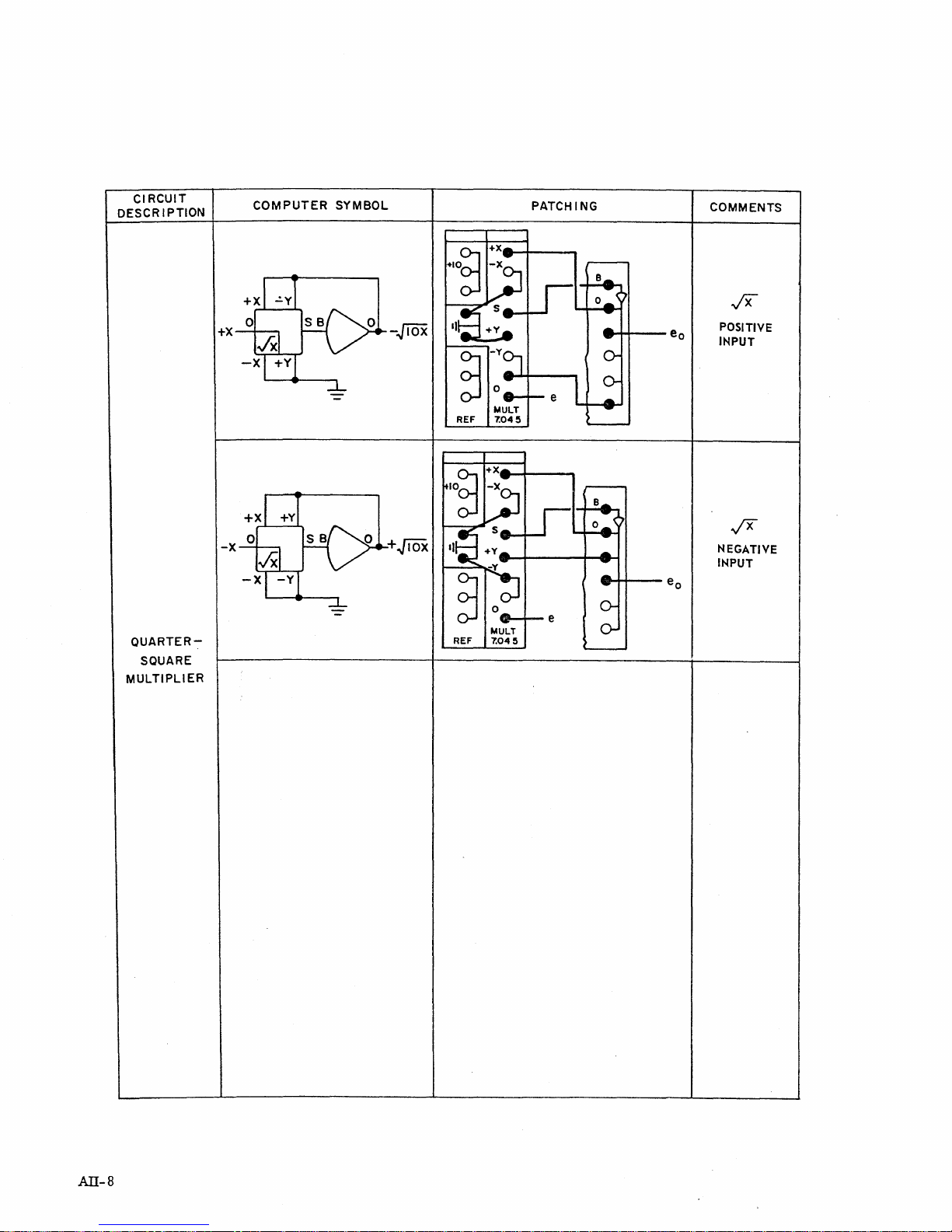
CIRCUIT
OESCR I PTION
COMPUTER
SYMBOL
PATCHING
COMMENTS
QUARTER-:-
SQUARE
MULTIPLIER
+x
+x
--+-+---eo
~-
.......
POSITIVE
INPUT
ft
NEGATIVE
INPUT
ATI-8

CIRCUIT
DESCR I
PTI
ON
COMPUTER
SYMBOL
-x
10
PATCHING
COMMENTS
X2
2
POSITIVE
INPUT
16.101
X2
DFG
CIRCUITS
OSXS+IO
-IOSXSO
-xlxl
10
tiN
+X-.j.-..
s
o
X2DFG
-x
5
o
fiN
---...-
---+--
...
...
...
-+----+--a~
X2
(0
X2
B
X2
+-
10
NEGATIVE
INPUT
X2
BI-POLAR
INPUT/OUTPUT
-IOSXS+IO
01
-x
X
2
-IOSXSO
+ViOX
-x
o
._-t---------'
tiN
...
4 .......
5
...
-4----'
xlxl
(0
JX
B
NEGATIVE
----lo.;::~=x
INPUT
DIODE
VOLTAGE
DROP
ATI-9

CIRCUIT
DESCRI
PTiON
COMPUTER
SYMBOL
+X
PATCHING
COMMENTS
.jX
POSITIVE
INPUT
16.101
2
X
DFG
CIRCUITS
(CONTINUED)
0$
X$
-IO$X$+IO
+10
x
x
-v1Ox
-=i=~--x
DIODE
VOLTAGE
DROP
2
BI-
POSITIVE
81-
NEGATIVE OUTPUT
x
POLAR
x
POLAR
INPUT
OUTPUT
2
INPUT
-IOSX
$+10
AlI-lO
x
X~y2
10
Y
IN
s._+-----
O._~------r--~
+IN
s
__
+-
...
.....
X2_Y2
10
x2_
y2
X INPUT
Y INPUT POSITIVE
NEGATIVE

CI
RCUIT
OESCRI
PTION
COMPUTER
0
1
-2LN
SYM
BOL
+5LOG1010X
.921
lOX
+X
-x
PATCH
-2LN
ING
lOX
COMMENTS
LOG X
POSITIVE INPUT
(BASE
10
AND
NATURAL)
16.126
LOG X
OFG
CIRCUITS
SI
-X
LOG
°2
-t5LOG1010X
.921
+2LN
lOX
I X
+io
ANTI
LOG
IO
+IN
X
0
1
-lANTILOG
10
10
+5
151
I~I
5
-X
IN
LOG
__
lOX
IO
0
0
+IN
0
-1-------,
+2LN
10~
LOG X
NEGATIVE INPUT
10
(BASE
ANTILOG X
NEGATIVE INPUT
ANTILOG X
POSITIVE INPUT
AND
NATURAL)
(BASE
10)
(BASE
10)
-.!..ANTILOG
lO
I~I
10
5
AII-ll

CIRCUIT
DESCRIPTION
16.126
LOG
X
DFG
CIRCUITS
(CONTINUED)
COMPUTER
.4343
S2
LOG
+X
.4343
-10
SYMBOL
PATCHING
COMMENTS
-x
ANTILOG X
NEGATIVE INPUT
(NATURAL BASE)
+x
INo
__
-'-----_
X
-IN
o
o
-16ANTILOGe\%I-
.....
,....j
-10
C
+A(lOX)
ANTILOG X
POSITIVE INPUT
(NA
TU
RAL
BAS
E)
AII-12
LOG
10
lOA
c
X
NEGATIVE INPUT
C
-X
-ex
-Ae
IN
+10
EXPONENTIAL
FUNCTION
o
II
o

CIRCUIT
DESCRIPTION
COMPUTER
r----.....,.°l
+ B
VDFG 8
°2
05X5+10
SYMBOL
2
PATCHING
COMMENTS
+X
f(
16.308
OR
16.310
POSITIVE X
+X
NEGATIVE X
VDFG
CIRCUITS
( FIXED AND
VARIABLE
BREAKPOINT
UNITS)
±X
-IO::;X::;O
-IO~X~+IO
;O--
.......
-f(X)
f(X)
±X
16.309
OR
16.311
e--+t---
f
(X)
f(X)
BI-POLAR
POSITIVE
f (X) MONOTONIC
AND
INCREASING
3
(X I Tan
X,
X
X,
ETC.)
AII-13/l4

CIRCUIT
DESCR
IPTtON
COMPUTER
SYMBOL
COMMENTS
RELAY
COMPARATOR
6.143
Ei~~~-------------~
-10
-Ej
....0----
Eo
----..3II~--Ei
Eo
ABSOLUTE
VALUE
Eo
DEAD
ZONE
Ej--~-------------~
-10
A
10
-10
---..
r--_
10
-10
A
10
---~~:""--Ei
\-+2A
BACKLASH
AIl-15
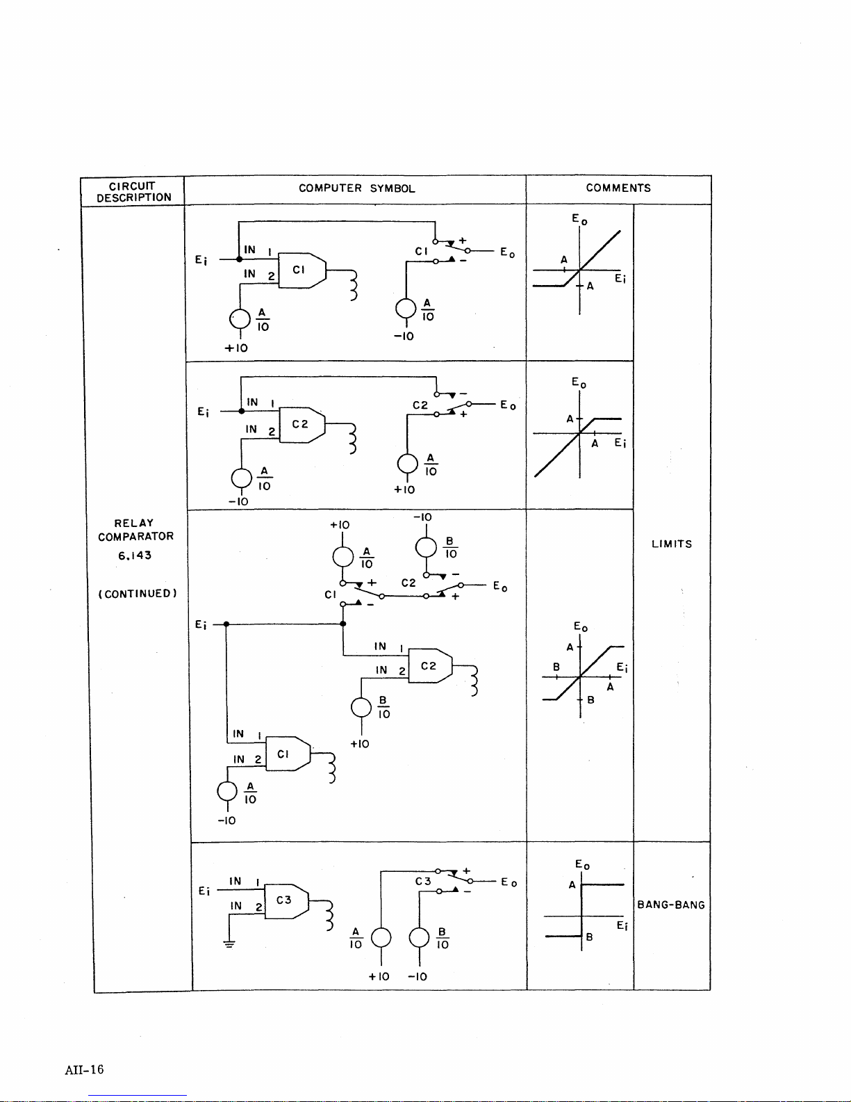
CIRCUIT
DESCRIPTION
COMPUTER SYMBOL
COMMENTS
Eo
RELAY
COMPARATOR
6.143
(CONTINUED)
Ej
Ej
Ej
+10
-10
CI
¢:-
-10
C2
A
10
+10
-10
+(0
~A
10
~EO
CI +
~~
(0
Eo
Eo
Eo
LIMITS
Eo
-10
Ei~
AII-16
+10
A
10
+10
*;
BANG-BANG
-10

CIRCUIT
OESCRI
PTION
COMPUTER
LTH
B
SYM
UN
LTH
ELECTRONIC
COMPARATOR
40.538
B
x
Y
DIG'
DIGITAL GATE I
UN
LTH
LTH
DIG
I
o
COMPARATOR

PATCHING
COMMENTS
DIGITAL GATE 2
ELECTROHI~
LATCH
IIP:JT
ELECTRONt~
ELECTRONIC
UNITY
ELECTRON!':
COMPARr.~~
vrU7AL
BINARY
DIRECT
:'.1"PARATOR
CI
~I"?UT
.l.1';,.nG
GAIH
lo-t"LOG
OUTf-~~
7--:~O.COMPARATOR
X-vO,~OMPARATOR
~')MPARATOR
(BINARY
I
(+!5VJ)
1WITCH
-#
I
INPUT
(GRD)
INPUT
SWITCH
I)
INPUT
SWITCH
I)
;I¥ITCH # I{
>MPLIFIER
AMPLIFIER
NPUT
(X+Y)
BINARY
-BINAR ( OUTPUT
-------
-------
v/.
OUTPUT
-----
__
--
AS SHOWN
LEVELS
ELECTRONIC
UNLATCH
o
[GRO])
ELECTRONIC
BINARY
I OUTPUT
ELECTRONIC
DIGITAL
DIRECT
ANALOG
(SWITCH
2)
UNITY
GAIN
INPUT
(SWITCH
ELECTRONIC
}
OUTPUT
COMPARATOR
OUTPUT
REVERSED
COMPARATOR
INPUTCBINARY
COMPARATOR
(+5V)
SWITCH
INPUT
INPUT
ANALOG
2)
SWITCH
AMPLIFIER
AMPLIFIER
--------->1.-
#2
ELECTRONIC
COMPARATOR AND
# 2
SWITCH
CIRCUIT
PATCHING
----------~
DIG
I
B
Eo
ELECTRONIC
SELECTOR
SWITCH
ATI-17
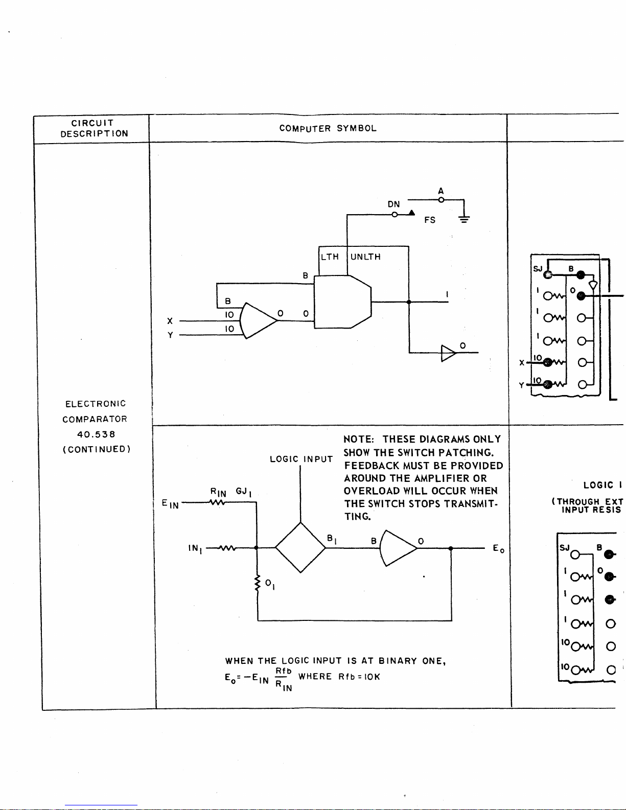
CIRCUIT
DESCRIPTION
COMPUTER SYM
__
lTH
UNlTH
B
.-J---
...........
BOl
A
--~D~N_~
ELECTRONIC
COMPARATOR
40.538
{CONTINUED}
x
Y
----~~
o 0
lOGIC
IN PUT
o
NOTE: THESE DIAGRAMS
SHOW
THE
SWITCH PATCHING.
FEEDBACK MUST BE PROVIDED
AROUND
OVERLOAD
THE
TING.
THE
AMPLIFIER
WILL
OCCUR
SWITCH STOPS TRANSMIT-
B
o
ONLY
OR
WHEN
lOGIC
{THROUGH
INPUT
SJ
REStS
I
EXT
•
o
WHEN
Eo=
-E
THE
IN
lOGIC
Rfb
RIN
INPUT
WHERE
Rfb
IS
AT
= 10K
BINARY
o
ONE,
o

PATCHING
DISPLAY
"10
Y
zO
X,O
X
20
COMMENTS
"30
LTHO
..A.O
UNO
LTH
REMAINDER OF
PATCHING
REQUIRED.
AS
SELF-LATCHING CIRCUIT.
DIG 1 TERMINAL
TO
WHEN
X+
Y>
GOES
+5
VOL TS. OUTPUT
REMAINS IN THIS
STATE
AllY
UNTIL
MANU-
RESET WITH
FUNCTION SWITCH.
0,
REMAINDER OF
PATCHING
REQUIRED.
AS
CI
RCUI
BASIC
FOR
A GAIN
T
OTHER THAN
UNl TY THROUGH
AN
ELECTRONIC
SWITCH

APPENDlxm
(a)
for
be
Com~,
NO.
AMPLIFIER
The
to.llo'Wing
simulatillg
round
in
Inc.,
transfer
Jackson,
New
BODE
CmCUITS
Table
A.S.:
York,
PLOT
E.
FOR
SIMULATING
contains
functions.
"Analog
1960.
B
I
TRANSFER
examples
A more
Computation",
TRANSFER
FUNCTION
~"'-
ot
complete
I~V
0-
A
FUNCTIONS
amplifier
MCGrall-9Hill<B.ook
CONSTANTS
-E
0
circuits
llsting
TIME
may
GAINS
1:
t
t
1
I
2
o~-
0---------
K~
T
E·
~
1
0-f"'-
AI~V
1
1
+
Tp
K
+
Tp
B
~-Eo
B
T=.1
.A
T
. -
B
K=-
A
1
A
A=B=-
A=-
B =
1
T
1
T
AK
0-
A
1
A=-
T
B • 1
1
Tp
+
Tp
3
o~
T
1
= -
A
0---------
4
~T
T
l
K
1
K;e
+
Tp
T--
K =
1
A
BT
A=-
B
II:
1
T
AK
AIll-I

NO.
BODE
E.
I
PLOT
TRANSFER
FUNCTION
B
TIME
CONSTANTS
GAINS
5
(b)
The
values
extensive
Fifer,
tor
s.
o
tollCNing
some
listing
usetul
: "Analog
NO.
SHORT-CKT.
I.
A
table
contains
networks
I1lB.y
be
round
Computation
Yss
ADMITTANCE
1
-
A
u
tor
in
•
the
short-circuit
simulating
Jackson,
(See
Bibliography.)
--A../\/'v-
D
transfer
A.S.:
NETWORK
R
1'2--
1'.3.
admittance
IIAnalog
1
B-CD
1
-
B-C
and
tunctions.
Computation",
A=R
component
A more
and
1 +
fir
2.
3.
AIIl-2
A
A
(1
1
+ pT)
-Q-
R
~
T
R
C
R
A=R
T =
A
r:a
T
--
RC
2ft
RC'
2

NO.
Yss
SHORT-CKT.
ADMITTANCE
NETWORK
4.
5.
6.
7.
8.
1(1
A ,
+pT)
..
pSI'
e < 1
1(1
A 1 +
e < 1
1 1 + pSI
..!.
A 1 +
,l1+pGr
A 1 +
C)
< 1
1 +
e <
"1
A 1
+pT)
pT
per
pr
-+
pT
pSI
e < 1
R2
c
R R
A =
R1 + R2
T = R2C
R1
A =
R1
T = (R
A = 2ft1
T = (R
e = 2
A = 2ft
T =
e =
+ R
1
+ -2 ) C
2
2R
2R2 + R1
~
(C1 + C2)
2C
2
C'i
+ C
R
2
2
) C
2
1 «
1+pTl)
A
9.
(1+pT2)
(1+pT3~
)
Am-3

The
following
cations.
ever,
that
GENERAL
This
these
list
of
is
by
references
written
no
material
means a complete
will
in
APPENDIX
BIDLIOGRAPHY
is
categorized
bibliography
turn
indicate
other
IV
by
both
of
material
general
material
and
available.
references
specific
It
of
the
fields
is
felt,
type
of
appli-
how-
desired.
Rogers,
Hill
Jackson,
Fifer,
Cheng,
S:
D.
Reading,
Karplus,
Mathews,
and
New
Heizer,
Potentiometers",
A.
E.
and
Book
Company,
A.
S.:
"Analog
"Analogue
K.:
"Analysis
Massachusetts,
W.
J.:
"Analog
M.
V.,
and
Passive
Networks",
York), 7 -12
L.
E.,
and
Connolly,
Inc.,
Computation",
Computation",
of
Linear
Simulation",
Seifert,
(March
S.
J.
Abraham:
J.
Assoc.
T.
W.:
New
1959
W.
Proc.
1955)
"Analog
York,
McGraw-Hill
McGraw-Hill
System",
McGraw-Hill
W.:
"Transfer
1955
Western
"Transfer
Compo
Mach.,
Computation
1960
Book
Book
Addison-Wesley
Book
Function
Joint
Function
3(3):
186
in
Engineering
Company,
Company,
Publishing
Company,
Synthesis
Computer
Simulation
(July
1956)
Inc.,
Inc.,
Inc.,
with
Conf.,
by
Means
Design",
New
New
York,
Company,
New
Computer
(published
of
McGraw-
York,
1960
1961
Inc.,
York,
1958
Amplifiers
by
IRE,
Amplifiers
and
AERODYNAMICS
"Aircraft
"Human
Performance
C.
C.,
March
Pilot
D.
T.,
Proceeding
1-3,
1955,
Dynamic
and
Weir,
of
p.
Response
D.H.,
August, 1958; ASTIA
Studies
the
78
No.
on
an
Western
in
Wright
AD
130.
Electronic
Joint
Flight
and
Air
Development
988
Analog
Computer
Simulator",
Computer",
Conference,
Seckel,
Center,
WADC
Wadel,
presented
E.,
Hall,
Technical
L.
B.,
at
Los
I.
A.
Report
and
Angeles,
M.,
Wan,
McRuer,
57-520,
AIV-l

"Rigid
Missiles",
Angeles,
Body
Equations
Mangnall,
CCLA
of
Report
Motion
J.
N.,
No.3,
for
Use
Electronic
El
Segundo,
in
Analog
Associates,
Computer
Calif.,
Inc.,
March
Studies
of
Computation
18,
1957
Symmetrical
Center
Spinning
at
Los
CHEMICAL
"Analog
E.
W.,
Computer
Society
"Analog
Simulation
Spencer,
ment-Automation
ember
"Analog
Computing
T.J.,
"Application
Franks,
Meeting,
"Analogical
Automation,
A:t\TD
INDUSTRIAL
Simulation
Instrument
of
America
E.
H.,
26-30,
1960,
Industrial
of
General
R.
G.,
June,
Computing
Vol.
ENGINEERING
of a
Society
Paper
of
No.
of a Chemical
1960
Proceedings
Conference
preprint
in
the
Chemical
and
Engineering
Purpose
and
OTBrien, N.
1957
Devices
22,
June,
Chemical
America
56-7-2
Reactor
and
No.
and
Analog
G.,
in
the
1949,
Reactor",
Journal,
Temperature
of
Instrument
Exhibit,
72-NY60,
Petroleum
Chemistry,
Computer
American
Petroleum
p.
497
Batke,
Vol.
4,
JanuarY,1957,
Control
SOCiety
Vol
15,
pp.
72-NY60-1-72-NY60-9
pt.
of
TI,
Industries,
Vol.
50,
1958,
to
Unsteady
Institute
Industry",
of
MorriS,
T.
L.,
Franks,
System",
America
presented
Past
and
p.
1631
State
Distillation
Chemical
W.
R.
p.14,
Mayer,
15th
Annual
at
New
York,
Present",
Engineers,
L.,
Instruments
G.,
and
James,
and
Instrument
F.
X.,
and
Instru-
Sept-
Williams,
Calculations",
Seattle,
and
AIV-2
"Modern
and
76,
Computer
Spergel,
No. 31,
P.,
July,
CONTROL SYSTEMS
"Analog
"Optimization
Computer
F.
D.,
p.
143
IRE
Transactions
IRE
Transactions
by
Random
Applications
Analysis
Transactions
1957,
Search
on
Electronic
for
the
pp.
in
on
Electronic
Design
of
the
105-109;
Predictor
on
the
Analog
Computers,
of
Steel
American
discussion,
Design",
Computers,
Computer",
Vol.
Mill
Control
Institute
pp.
Bates,
Vol.
EC-8,
Systems",
of
Electrical
109-110
M.
R.,
EC-6,
Munson,
No.2,
Bock,
No.3,
J.
K.,
June,
Reider,
Engineers,
D.
H.,
and
September,
and
Rubin,
1959,
p.
J.
E.
Vol.
Powell,
200
,
1957,
A.1.,

"Analog
Proceedings
N.
Report
Computer
J.,
October
57GL351,
Study
of
the
16-18,
of
Sampled
Computers
1957,
November
p.
15,
Data
in
Control
71,
1957
Systems",
Systems
and
General
Chestnut,
Conference,
Electric
H.,
Dabul,
presented
Technical
A.,
and
at
Atlantic
Information
Leiby,
Series,
D.,
City,
"Analysis
"Missile
"Analog Study of
"Modern
"Jet
of a
actions
System
putation
Vol.
15,
Computer
Spergel,
Pt.
II, No. 31,
Engine
of
the
1957,
Non-linear
on
Automatic
Linearization",
Center,
Boiler-Reactor
No.5,
P.,
Transactions
Simulation
National
p.
15.0
Control
Control,
PCC
Report
May,
1957,
Analysis
July,
1957,
for
Engine
Simulation
Favreau,
Interaction",
p.
for
the
of
pp.
Council,
DATA ANALYSIS AND PROCESSING
System
Vol.
No. 69,
84
Design
the
American
105-109;
Control
presented
for
Stabilizing a .Missile",
PGAC-3,
R.
Princeton,
R.,
November,
Electronic
N.
Borner,
of
Steel
Mill
Institute
discussion,
Development
at
.Washington, D.
J.,
November
E.
F.,
Control
of
Electrical
pp.
Work",
Atran,
1957,
p.
Associates,
and
Cassidy,
Systems",
109-110
Sherrard,
C.,
L.,
8
Inc.,
12,
1956
B.
F.,
Reider,
Engineers,
E.
S.,
December
mE
Trans-
Princeton
Nucleonics,
J.
E.,
Vol.
76,
Proceedings
10-12,
Com-
and
"Simulation
Byck, D.
port
"Direct
Research
September,
"The
F.
"A
Multipurpose
cations",
No.4,
of
Linear
M.,
No. 91,
Measurement
Council
Generation
C.,
Electronic
Diamantides,
December,
Electronic
El
Segundo,
1959; ASTIA No. AD 230 392
of
Fourier
Electronic
Constant-Coefficient
ASSOCiates,
Calif.
of
Power
of
Canada,
Spectra
Mechanical
by
Transforms
Engineering
Switch
N.
1956.
D.,
p.
(London),
for
IRE
197
Analog
Transactions
Systems
Inc.
an
Analog
Engineering
and
Coefficients
Vol.
Computer
by
the
Weighting
Computational
Computer",
Report
on
32, No. 390,
Simulation
on
Electronic
Center
an
Analogue
August
Function
at
Los
Wonnacott,
MK-5,
Ottawa,
Computer",
1960,
and
Autocorrelations
Computers,
Technique",
Angeles,
T.H.,
Canada,
pp.
496-498
Vol.
PCC
Re-
National
Harbert,
Appli-
EC-5,
AIV-3
"Analog
F.
p.
Computer
D.,
IRE
143
Applications
Transactions
in
Predictor
on
Electronic
Design",
Computers,
Bates,
Vol
M.
EC-6,
R.,
Bock,
No.3,
D.
H.,
and
September,
Powell,
1957,
"Evaluation
and
"Random
of
bourg,
"Transport
of
Pfeffer,
Optimization
the
Second
September
Delay
Corporation,
"Analog
D.
M.,
Computer
Technical
ASTIA No. AD 246
"Simulation
National
1956,
p.
Complex
1.,
International
Simulation
Atomic
Mechanization
Wright
Note
of
Military
Simulation
1.1
Statistical
1956
by
1-6,
Air
Development
59-344,
530
Vehicle
Conference
IRE
Convention
Analog
Analogue
1958,
Circuits",
Power
Project
Functions
Techniques",
Computation
pp.
437
Single,
Division,
of a
Tilt-Wing
Division,
1365,
Suspension
Proceedings,
by
an
Analog
Record,
Vol.
Favreau,
Meetings
-443
C.
H.,
and
Report
WAPDT-38
VTOL
Air
Research
Aircraft",
Wright-Patterson
Systems",
Sattinger,
presented
Computer",
4,
pt.
4,
R.
R.,
Stubbs,
and
Air
at
Favreau,
March
and
19-22,
Franks,
(Brussels),
G.
S.,
Balsink,
Development
Force
I.
Dallas,
J.,
Base,
and
Texas,
R.
R.,
1956,
R.,
Proceedings
presented
Westinghouse
E.
B.,
and
Command,
Ohio,
July,
Therkelson,
January
Low,
p.
31
at
Stras-
Electric
Sovine,
WADD
1960;
E.
B.,
19-21,
H.,
"Real-Time
"Operational
"Dynamic
ELECTRICAL
"Determination
AIV-4
Automobile
Conference,
Analog
Structure",
Analysis
Bulletin,
J.
H.,
trical
No.6,
Fahrnkopf,
Engineers,
Simulation",
presented
at
Simulation
Clymer,
of
an
Aircraft
A.
B.,
Electronic
ENGINEERING
of
Impulse
C.
Stresses
D.,
Vol. 75, pte
San
Francisco,
of
the
mE
Transactions
Arresting
ASSOCiates,
Within
and
Steele,
Ill,
Kohr,
R.
Vibration
Gear
Transformer
J.
H.,
1956,
H.,
Proceedings
May
3-5,
of a
on
System",
Inc.,
Long
Transactions
p.
1267
1960,
p.
Beam
and a Rectangular
Electronic
Hans,
Branch,
Windings
of
the
285
Computers,
M.
N.
J.
by
of
the
American
Western
Multicellular
Vol.
W.,
PACE
Computers",
Institute
Joint
Computer
EC-8
Application
McWhirter,
of
Elec-
"The
Use
of
Analogue
w.
C.,
Transactions
April,
ELECTRONICS
1956,
pp.
Computers
of
the
238-242
in
Power
American
System
Institute
Studies",
of
Electrical
Van
Engineers,
Ness,
J.
E.,
Vol
and
75,
Peterson,
pt.
III,
"Solutions
Computers
May,
"Far
Field
Rubin,
Vol.
"On
the
Solution
Norris,
les,
Associates,
FLUID
"Analog
HUMAN
MECHANICS
Horowitz,
of
Partial
with
1952,
p.
Antenna
A.
I.,
15,
1959,
of
A.,
August
Computer
FACTORS
19-22,
M.,
Integral-Differential
Storage
163
Pattern
and
Landauer,
pp.
Sine
1958
Inc.
Computation
Construction
and
Devices",
Calculations
995-1011
Microwave
mE
WESCON
1958,
Reynolds,
J.
pp.
of
Equations
Wang,
by
P.,
Proceedings
Problems
Convention
70-85,
Center
Conformal
C.H.
and
at
,Journelof
C.
C.,
Means
of a General
by
an
Record,
Microwave
Los
Angeles,
Maps
Applied
of
Electron
Project
of
the
Analog
Vo1.2,
in
Fluid
Dynamics
Cyclone,
Purpose
National
Computer",
pt.
1,
Applications
October
Dynamics",
Physics,
27-28,
Using
Symposium
Analog
Electronics
Byck,
presented
Seminar,
1960
Tomlinson,
Vol.
26,
Analogue
II,
Computer",
Conference,
D.
M.,
and
at
Los
Electronic
N.
1955,
p.
April-
Ange-
P.,
229
"A
Study of
Analog";
"Analog
Electronics,
MA
THEMATICS
"A
1vietJlOd
L.,
p.
the
Mechanism
Warner,
Computer
of
Computing
Mathematical
194
Aids
Vol.
of
Pressure
H.R.,
32,
Tables
Circulation
Heart
Ailment
October
Eigenvectors
and
Diagnosis",
2,
1959,
and
Other
Wave
Distortion
Research,
pp.
Eigenvalues
Aids
to
by
Vol.
5,1957,
Skinner,
56-59
on
an
Computation,
Arterial
R.
L.,
Analog
Vol.
Walls
Using
p229
and
Gehmlich,
Computer",
13,
No.
67,
an
Electrical
D.
K.,
Neustadt,
July,
1959,
AIV-5

"A
Use
of
Case
October
Analog
Institute
27,
Computer
of
Technology,
1959;
ASTIA
in
Antenna
No.
Pattern
Scientific
AD 227
Report
253
Studies",
No.6,
Brammer,
F.
E.,
AFCRC-TN-59-579,
and
Wen-Hsiung
Cleveland,
Ko,
Ohio,
"Plotting
tion
"The
Use
Meissinger,
at
San
PHYSICS
"A
Time-Sharing
Computer
"Analog
Nuclear
in
p. 48
"Analog
craft
Results
of a Quadratic
Bulletin,
of
Parameter
H.
Francisco,
Analog
Conference,
Representation
Power
Control
Systems
Simulation
Corp.,
Report
No.
F.,
Plants",
in
10,
Electronic
Influence
Proceeding
May
3-5,
Computer",
presented
of
Heat
Carteron,
Conference,
Real-Time
GER-7491,
Regression
Associates,
Coefficients
of
the
1960,
p.
Reihing,
at
Exchange,
J.
presented
of
Xenon
Akron,
Analysis",
in
Western
181
J.
San
Francisco,
Application
M.,
and
at
Poisoning
Ohio,
Rubin,
Inc.,
Computer
Joint
V.,
Jr.,
to
Deloux,
Atlantic
in a Nuclear
April,
A.
Long
Branch,
Analysis
Computer
Proceedings.
March
the
3-5,
Simulation
G.,
City,
1956
I.,
et.
aL,
N.
J.
of
Dynamic
Conference,
of
1959,
of
Proceedings
N.J.,
October
Reactor",
.~~CE
the
Western
p.
341
Heat
of
16-18,
Goodyear
Applica-
Systems",
presented
Joint
Exchangers
the
Computers
1957,
Air-
of
POWER
"The
PLANTS
Derivation
Data",
Wolin,
January
AND
of
19-21,
PROPULSION
Simulators
L.,
National
1956,
p.
of
14.1
AIY-6
SYSTEMS
Gas
Turbine
Simulation
SIMULATION
and
Other
Conference
PhYSical
Systems
Proceedings,
from
presented
Experimental
at
Dallas,
Texas,
 Loading...