

Page 1

ANALOG/HYBRID
COMPUTING
SYSTEM
REFERENCE
HANDBDDK
Page 2

ANALOG/HYBRID
COMPUTING
SYSTEM
©
ELECTRONIC
ASSOC1ATES.
INC.
t968
•
PRINTED
IN
U.S.A
REFERENCE
••
PUBL.
NO.
00
800.2055.0
HANDBDDK
•
MARCH
'968
Page 3

The
table
Unless
tenance
tem.
below
otherwise
handbooks
lists
other
indicated
directly
RELATED PUBLICATIONS
publications
by
title
applicable
which ma.y
or
footnote,
to a particular
all
be
of
interest
are
maintenance
system
are
to
the
readers
handbooks. Note
normally
supplied
of
this
with
manual.
that
main-
the
sys-
Title
Handbook of Analog Computation
Basics
580
580
of
Parallel
Reference
Console
Hybrid
Computation
Handbook
Components Manual
580 Computing Components Manual
580 Logic
580/680
TR20/TR48
Expansion
Digital
Repetitive
Group
Voltmeter,
Operation
Model
Display Units,
Models 34. 034 and 34. 035
26.268
Publication
00 800. 0001-3
07
800.0016-0
00
800.2055-0
00
800.2056-0
00 800. 2057
00
800.2058-0
00
800.2059-0
00 800. 2024-1
Number
-0
Page 4

In
order
to
enable
and efficiently, we
us
to
request
1.
Please
the
scription
items
lays,
process
your
specify
basic
such
transformers,
NOTIC
your
requests
conformance
the
type
unit
as
well
of
the
part
as
potentiometer
for
with
number
as
the
when
inquiring
precision
E
spare
parts
the
following
and
serial
EAI
part
about
assemblies
resistors,
and
procedure:
number
number
replacement
or
cups,
etc.
replacement
of
and
dere-
items
quickly
2. When
Your
and
It
aid
is
cooperation
in
assuring
the policy
in
supplying
that
of
Electronic
ble to the requirements
of
prohibitive costs
ponents,
etc.,
custom design, by substituting new components, modifying standard
wherever
this instruction manual, which has been written to
concur in
fied
its
content with the equipment supplied. It
person will find the manual a fully adequate guide in understanding, operating, and
inquiring
solvers,
please
specify
ment with which
Console,
Serial
clude
under
No. 000,
the
which
the
the
correct
Associates,
of
the individual customer. This
necessary
about
networks,
the
the
Type
8811,
etc.
purchase
the
equipment
required
items
to
expedite conformance with requirements.
items
printed
serial
units
Memory
If
at
order
information
are
supplied.
Inc. to supply equipment patterned as closely as
as
servo
circuit
numbers
are
to be
Module,
all
possible,
or
the
EAI
was
originally
cover
is
multipliers,
assemblies,
of the
major
used,
such
Type
please
project
re-
etc.,
equip-
as:
4.204,
in-
number
procured.
will
speed
the
proceSSing of
is
accomplished, without incurring the
standard equipment, may not
felt, however, that a technically quali-
taining the equipment actually supplied.
your
requests
possi-
com-
As a result,
entirely
main-
M226-S
Electronic
the
right
or
to
ments
ASSOCiates, Inc.
to make changes in design,
make
additions
in
its
product
any obligation upon
them
on
products
tured.
to
or
improve-
without
itself
to
previously
reserves
imposing
install
manufac-
PRINTED
IN
U.S.A.
Page 5

UNITED
STATES
AND
CANADIAN
OPERATIONS
Marketing Division
EASTERN REGION
Eastern Reaional Office: West Long Branch, N. J. 07764, Tel: 201-229-1100, TWX 710-722-6597, Telex 01-26655, Cable: PACE
West Long
Branch.
N.
J. 07764
Special System
PACE
Customer
Long
Northeastern
Syracuse
455-5521
SOUTHEASTERN REGION
Southeastern
CENTRAL REGION
Central
Cleveland
SOUTHERN REGION
Southern
Houston
~~I~~J~I!~8~!;~~~t
WESTERN REGION
Western Regional Office: 1500 East
San Francisco
Northwestern
EASTERN REGION
Eastern U.S. Headquarters: West Long Branch, N. J. 07764, Tel: 201-229-1100, TWX 710-722-6597, Telex 01-26655, Cable:
PACE
Northeastern
Princeton,
Resident
SOUTHEASTE~N
Southeastern
CENTRAL REGION
Central
Cleveland
Resident
SOUTHERN REGION
Southern
Houston
Huntsville
Telephone: 205-881-7031
Resident
WESTERN REGION
Western U.S. Headquarters: CUSTOMER REPAIR FACILITY, 1500 East
Telephone: 213-322-3220, TWX 910-348-6284
Western
Telephone: 213-322-3220, TWX 910-348-6284
San
Resident
Colorado/Ryan
CANADA
Toronto
Princeton
452-2900
Los Angeles Analysis and
322-3220, TWX 910-348-6284
San
TWX 910-373-1241
Washington,
Houston
Engineerine
PACE
Manufacturing
PACE
Instrument
07740
Pacific
Scientific
UNITED KINGDOM & SCANDINAVIA
Electronic
PACE
Northern
SWEDEN
EAI·Electronic
10064, Cable: PACE STOCKHOLM
EUROPEAN
EAI·European
18-40-04,
FRANCE
EAI
GERMANY
EAI·Electronic
AUSTRALIA & NEW ZEALAND
EAI·Electronic
Victorian
JAPAN
EAI·Electronic
Telex: 7814285,
~~~~ro;~cR~~~O~i~r~L.
MEXICO
EAI·Electronic
PACEMEX
Department:
West Long Branch, N. J. 07764
Services: West Long
Branch,
N. J. 07764
District
District
Regional Office: 12260
Regional Office: 33166 Des Plaines Ave., Des Plaines,
District
Regional
District
District
District
West Long Branch, N. J. 07764
District
New
Jersey: U.S. Route No.
Field
Engineers: Bedford,
Regional Office: 12260
Regional Office: 3166 Des Plaines Avenue, Des Plaines,
District
Field
Engineers:
Regional
District
District
Field
Engineers: San
U.S. Headquarters: CUSTOMER SERVICES FACILITY,
Francisco
District
Field
Eneineers: Edwards,
Aeronautical,
Office:
Allan
Analysis
Francisco Analysis and
D.
C.
Analysis
Department:
West
Long
Department:
West
Long
Division:
Data Systems,
Instruments
Associates,
Burgess
Hill
Area Office: Roberts House,
Associates·AB: Hagavagen 14, Solna 3, Sweden,
CONTINENT
Continental
Telex:
Electronic
Associates SARL: 72-74, rue de la
Associates GMBH: 5100 Aachen, Bergdriesch 37,
Associates, Pty.,
Office: 34 Queens Road,
Associates (Japan),
Cable: EAIJAPACE
ASSOCiates,
~~t::,e~~1~~g't.u~:~~~
United
Kinedom
5101·10,
Telex:
Australian
871·183, Cable: PACE BURGESS
Computation
West Long Branch, N. J. 07764,
Branch,
N. J. 07764, Tel: 201-229-1100, TWX 710-722-6597, Telex 01-26655, Cable: PACE West
Office: 875 Providence Highway, Dedham,
Office:
Pickard
Building,
Wilkins
Office: 6741 Ridge Road, Parma, Ohio 44129,
Office: 3514 Cedar
Office: 7007
Office:
Office: 4151
Office: 1107
Office: 875 Providence Highway, Dedham,
REGION
Office: 6741 Ridge Road, Parma, Ohio 44129,
Office: 3514 Cedar
Office: 7007
Office:
Office: 4151
Crawford Associates,
and
Computation
Analysis and
and
Computation
8ranch,
Branch, N. J. 07764
Long
Inc.:
Department:
Springs
Gulf
Freeway, Room 128, Houston, Texas 77017, Tel: 713-MI 4-3678
Holiday
Office Center,
Imperial
Middlefield
Northeast
I,
Mass./Florham
Wilkins
Detroit,
Michigan/Pittsburgh,
Springs
Gulf
Freeway, Room 128, Houston, Texas 77017, Tel: 713-MI 4-3678
Holiday
Office Center,
Antonio,
Texas/Alamogordo, New
Middlefield
California/Pasadena,
San Diego,
California
ANALYSIS
Center: U.S. Route No.
Computation
West Long
N. J. 07764
Branch,
Center: 1500 East
Computation
Computation
Center: 7007
Engineering and Manufacturing Division
Branch,
West Long Branch, N. J. 07764, Tel: 201-229-1100, TWX 710-722-6597, Telex 01-26655, Cable:
Other Departments, Divisions and Subsidiaries
N. J. 07740, Tel. 201-229-4400, TWX 710-722-6597, Cable: PACE West
644 Young Street, Santa Ana,
4151
Middlefield
INTERNATIONAL
Ltd.:
Burgess
Hill,
Sussex, England, Tel: Burgess
Manchester
Regional Office:
2.21-106, Cable: PACEBELG Brussels
Ltd.:
26
Albany
Melbourne
Inc.:
9th
Ltd.:
Burgess
Hill,
S.A. de C.V.:
~:g~~kE~n~r~~~~:;rnatiOnal,
Computation
Center:
Electronic
Center: 34 Queens Road,
SALES OFFICE
Tel:
201-229-1100, TWX 710-722-6597, Telex 01-26655, Cable:
Room 144-147, 5858 East
Avenue, Rockville,
Road, Room 211, Dallas, Texas 75219, Tel: 214-528-4920
Suite
Highway,
Road. Palo
45th
St., Room 323,
CUSTOMER SERVICES OFFICES
P.O.
Box 582,
Park, N.
Avenue, Rockville,
Road, Room 211, Dallas, Texas 75219, Telephone: 214-528-4920
Suite
Road, Palo Alto,
ltd.,
65
Center: 4151
Center: 12260
Gulf
N.
J. 07764, Tel: 201-229-1100, TWX 710-722-6597, Telex 01-26655, Cable:
Massachusetts
Maryland
Illinois
Tel:
2, 3322.
South
EI
Segundo,
Alto.
California
Seattle,
Massachusetts
Princeton,
J./Washington,
Maryland
Illinois
Telephone:
Pennsylvania/Dayton,
2, 3322
South
Mexico/Tulsa,
1500
California
California/Moffet
Martin
Ross
Avenue, Downsview OntariO, Canada, Tel: 416-636-4910
AND COMPUTATION CENTERS
I,
P.
O.
Imperial
Middlefield
Wi
IKins Avenue, Rockville,
Freeway, Room 128,
California
Road, Palo
Alto,
SALES & CUSTOMER
Road,
Altrincham,
Tel:
Centre
International,
Tombe
St., Leonards, N.S.W.
S.
C.
2,
Mori
Building,
ENGINEERING
Sussex,
England,
Darwin
#142,
COMPUTATION CENTERS
Associates, Ltd., Burgess
HILL
Melbourne
22nd Floor, Place Rogier,
Issoire,
Paris 14e, France, Tel: 535.01.07, Telex 27610
West
Australia,
Tel:
1·3 Shiba-Atago-cho,
AND MANUFACTURING
Tel: Burgess
Planta
Baja, Col. Anzures,
22nd
Floor, Place Rogier, Brussels
S.
C.
02026, Tel: 617-326-6756
Malloy
Road, Syracuse,
20852, Tel: 301-933-4100
60018,
Tel:
216-842-1840
California
New Jersey 08541, Telephone: 609-452-2900
East
Highway,
312-296-8171
Memorial
Parkway,
90245, Tel: 213-322-3124, TWX 910-348-6284
94303. Tel: 415-321-0363, TWX 910-373-1241
Washington 98105, Tel: 206-632-7470
02026, Telephone: 617-326-6756
D.
C./Baltimore,
20852, Telephone: 301-933-4100
60018, Telephone: 312-296-8171
216-842-1840
Ohio/Warren,
Memorial
Parkway,
Oklahoma/Houston,
Imperial
Highwa/,
Imperial
Highway,
94303, Tel: 415-321-0363, TWX 910-373-1241
Field,
California/Martin
Box 582, Princeton, New Jersey 08541, Telephone: 609·
EI
Segundo,
Road, Palo Alto,
Houston,
92705, Tel. 714-540-3610, TWX 714.546-3049
California
94303, Tel: 415·321·7801; TWX 910-373·1241
SERVICES
Hill
(Sussex) 5101·10, 5201-5, Telex: 87183, Cable:
Cheshire,
Tel:
Altrincham
Stockholm
82-40-96; 82·40·97, 83·38-60,
Germany, Tel: Aachen
Australia,
26-1329, Cable: PACEAUS,
2,
Tel: 43-7522, Cable: PACEAUS,
Minato·Ku,
Hill
(Sussex) 5101-10, 5201·5, Telex: 87183, Cable:
Hill,
Sussex, England, Tel: Burgess
Australia,
Tel: 26-1329, Cable: PACEAUS,
New
York
Huntsville,
Alabama
Md./Eatontown,
Michigan
Huntsville,
Alabama
Texas
EI
Segundo,
California
EI
Segundo,
Marietta
California
90245, Telephone: 213-
California
94303, Tel: 415-321-0363,
Maryland
Texas 77017, Tel: 713
20852, Tel: 301-933·4100
OFFICES
5426
Brussels
I,
Belgium,
26042;
26041,
Melbourne
Tokyo, Japan,
Mexico
5,
D.F.,
Tel:
I,
Belgium,
Tel:
13211,
Tel:
35801,
N.
J.
35801,
90245,
California
90245,
Corp., Denver,
MI
4·3678
Lone
Branch,
Telex
Stockholm
Tel:
Telex 832.676
Sydney
Tel:
433-4671,
28-55-13, Cable:
Brussels
Hill
Melbourne
315-
N. J.
Brussels
eai
18-40-04,
(Sussex)
d
Printed
In
U.S.A.
EAI
ADVANCED
PLonERS/SIMULATION
TION
SYSTEMS/TEST
SYSTEMS
ANALYSIS
AND
:LECTRONIC
AND
COMPUTATION
SYSTEMS/SCIENTIFIC
CHECK-OUT
SYSTEMS/MILITARY
ASSOCIATES,
SERVICES/ANALOG
AND
LABORATORY
AND
COMPUTERS/DIGITAL
INSTRUMENTSIINDUSTRIAL
INDUSTRIAL
RESEARCH
AND
INC.
Wul
COMPUTERS/HYBRID
PROCESS
CONTROL
DEVELOPMENT
L.a.,,,,,,,,,
SERVICES/FIELD
N_
ANALOG-DIGITAL
SYSTEMS/
PHOTOGRAMMETRIC
ENGINEERING
J=y
COMPUTATION
07764
EQUIPMENT/ANALOG
EQUIPMENT/
ANO
EQUIPMENT
AND
RANGE
INSTRUMENTA·
MAINTENANCE
DIGITAL
SERVICES.
Bulletin
No. IL-641D4-10
July,
1967
Page 6

CONTENTS
CHAPTER
CHAPTER
1 -
GENERAL
580
1.1
'GENERAL
1.2
OPERATING
1.3
KEYBOARD
1.4
ANALOG
1.5
THE
1.6
THE
1.7
READOUT
2 -
OPERATIONAL
2 . 1
INTRODUCTION
2.2
DUAL
2.3
QUAD
DESCRIPTION
ANALOG/HYBRID
DESCRIPTION
CONSIDERATIONS
PANEL
READOUT
AUXILIARY
..
PANEL
CONTROL
LOGIC-CONTROL
DEVICES
AMPLIFIERS
.....•.....•....•...•.......•...
DC
AMPLIFIER
DC
AMPLIFIER
AND
OPERATION
COMPUTING
OF
THE
SYSTEM
•..•.•••.•.•.••.•.••••••.
• . • • . • • • • • • • • • • • • • • • • . . . . • • •
••.••••.•••.•••.•...•..•
PANEL
AND
INDICATOR
•....•••••.•.•.•.
PANEL
••••.••
PATCHING
PATCHING
1-1
1-1
1-14
1-21
1-21
1-25
1-28
2-1
2-1
2-4
CHAPTER
CHAPTER
CHAPTER
3 -
ATTENUATORS
AND
3. 1 ATTE'NUATORS
3.2
4 -
4.1
4.2
5 -
FEEDBACK
LIMITER
INTEGRATORS
INTRODUCTION
INTEGRATOR
TRAYS
QUARTER-SQUARE
5. 1 INTRODUCTION
5.2
MODEL
0.7.0146
MULTIPLIERS
5.3
MODEL
0.7.0150
FEEDBACK
LTIMITERS
MULTIPLIERS
.•..•...•••••.•.••...•.••...
AND
0.7.0148
QUARTER-SQUARE
....•.•.•.•.•.•.•.•••.•••....•
QUARTER-SQUARE
MULTIPLIER
0
•••
....
3-1
3-1
4-1
4-1
5-1
5-1
5-8
i
Page 7

CONTENTS
(Cont)
CHAPTER
CHAPTER
CHAPTER
6 -
LOG X DIODE
FUNCTION
6. 1 INTRODUCTION
6.2
OPERATING
6.3
OPERATING
7 -
THE
7.1
INTRODUCTION
7.2
THE
7.3
TIlE
8 -
THE
8.1
8.2
e.3
8.4
INTRODUCTION
LOCATION
APPLICATIONS
SETUP
TRACK-STORE,
TRACK-STORE
D/A
MDFG
CONSIDERATIONS
INSTRUCTIONS
SWITCH
AND
ADDRESSING
PROCEDURE
GENERATORS
.•••.•.•.••.••••.••••••.••.••.•.
......... ' ............ .
D/ A SWITCH
CIRCUIT
.•.•.•.•••••...••.•.•.•..•..•.
TRAY
•••••.••••••••••••.•.
•.•....•••••••••.••••
6-1
6-1
6-1
7-1
7-1
7-1
8-1
8-1
8-1
8-1
ii
CHAPTER
CHAPTER
9 -
COMPARATORS
9 . 1
9 • 2
9.3
INTRODUCTION
THE
COMPARATOR
FUNCTION
10 -CONTROL
10.1
INTRODUCTION
AND
RELAYS
TRAY
FUNCTION
....•.•..•••...•.••.•.•.•..•.•..
RELAYS
9-1
9-1
9-1
• • • • • • • . • • • • . • • • . . . • • • • • • • . • • • • 10-1
Page 8

CONTENTS
(Cant)
CHAPTER
10.10
10.11
10.12
APPENDIX
10 -CONTROL
10.2
10.3
10.4
10.5
10.6
10.7
10.8
10.9
1 -
DVM
PATCH
VM
PATCH
IC
AND
SCOPE
PLOTTER
CHT
ON
RDAC
PATCH
A
SEL
TIMER
OVD,
ORR,
PP
PATCH
SIMPLE
PATCH
PATCH
PATCH
CIRCUITS
TRAY
(Continued)
TERMINAL
TERMINAL
OP
PATCH
TERMINALS
PATCH
PATCH
TERMINALS
TERMINAL
TERMINAL
TERMINALS
AND
TERMINAL
....•••••..•...••.••.•.•..
TERMINALS
TERMINALS
OLS
PATCH
..•...•........•...•.••..•.
USING
AMPLIFIERS
TERMINALS
AND
•..•.•.•...
ATTENUATORS
10-1
10-1
10-1
10-3
10-3
10-3
10-3
10-3
10-3
10-4
10-4
A1-1
APPENDIX
APPENDIX
APPENDIX
APPENDIX
APPENDIX
2
UNITY
3 -
TRANSFER
4 -
REPRESENTATION
5 -
LOGIC
6 -
BIBLIOGRAPHY
SCALING
PATCHING
. . . . . . . . . . . . . . . . . . . . . . . . . . . . . . . . A2-1
FUNCTION
OF
SIMULATION
CONSTRAINTS
.....••...
AND
NONLINEARITIES
0......
A3-1
A4-1
A5-1
A6-1
iii/iv
Page 9

Page 10

Figure
Number
1.1
580
Analog/Hybrid
ILLUSTRATIONS
Title
Computing
System
viii
1.2
1.3
1.4
1.5
1.6
1.7
1.8
1.9
1.10
1.11
1.12
1.13
Typical
Physical
Amplifiers
Feedback
DVM
Zero
Pre-Patch
Amplifier
Computer
Removal
Patching
Keyboard
Analog
Auxiliary
Readout
Pre-Patch
Layout
with
••.••••••••••..••••••.•••••••••.••••
Adjustment
Panel
Balance
Component -
of
Computing
Block
...•..••.•..•...••••..•..•....••.•....
Control
Panel
of
Four-Pin
Insertion
Control
Replacement
Panel
Panel
Field
the
580
Location
Field
Component
Bottle
Layout
Computer
Locations
Assignment
..••••••••••.•••.•••
.I
Plugs
Providing
Areas
1-2
1-3
1-5
1-6
1-8
1-9
1-10
1-12
1-13
1-15
1-22
1-23
1.14
1.15
1.16
2.1
2.2
2.3
3.1
Logic
Digital
Readout
580
Dual
Quad
Attenuators
Control
Patch
Device
Operational
and
Simplified
Amplifier,
Amplifier
and
Indicator
·Panel
Connectors
Amplifiers
Schematics)
Typical
Patching
Panel
(Patch
Patching
Configuration
Block
•••.••••.•••••.•••
Configurations
1-26
1-27
1-30
Layout
2-2
2-3
2-4
3-2
v
Page 11

Figure
Number
ILLUSTRATIONS
(Cont)
3.2
3.3
3.4
3.5
4.-1
4.2
4.3
5.1
5.2
5.3
5.4
5.5
Potentiometer
Feedback
Typical
Limit
Integrator
Typical
Integrator
Quarter-Square
Quarter-Square
Multiplier
.
Multiplier
Multiplier
Circuits
Limiter
Limiter
Curve
Integrator
Configurations
Patching
Patching
Patching
Used
Multiplier
Mu~~ip1ier,
Patching
Patching
Patching
Shown) .............................
Blocks
Patching
as a D/A
for
for
for
Block
Switch
Patch
Simplified
Multiplication
Division
Squaring
•• 0 ••••••••••••
Blocks
..............
(Two
Diagram
........
Squaring
3-3
3-5
3-5·
3-6
4-2
4-3
4-5
5-2
5-3
5-4
5-5
5-6
5.6
5.7
5.8
6.1
6.2
7.1
7.2
vi
Multiplier
Multiplier
Multiplier
Log X
Log X
Track/Store,
Track/Store
DFG,
DFG
Patching
Patching
Patching
Simplified
Patching
D/A
Circuit,
for
for
for
Switch
Simplified
Square
Multiplication
Division
Schematic
Patch
Root
Block
and
Patch
Diagram
Block
5-7
5-9
5-10
6-2
6-3
7-2
7-3
Page 12

Figure
Number
ILLUSTRATIONS
Title
(Cont)
7.3
7.4
8.1
8.2
8.3
8.4
8.5
8.6
8.7
8.8
9.1
9.2
10.1
Tis
Patching
D/A
Switch
MDFG
Effect
Typical
A
Typical
Control
Patching
Typical
DFG
Upper
Initially
Typical
Comparator
Ten-Segment
of
Setup
DFG
Function
Comparator
Tray
(Typical)
Patching
Terminations
Changing
Panel
Drawer
Horizontal
Twenty-Segment
and
Function
Patch
(Typical)
Function
Slope
(Lower
Requiring
Eleven-Segment
Patching
Panel
Pot 5 on
DFG
Drawer)
Slope
Function
Relay
DFG
Amplification
Function
Pa'tching
Output
Area
7-4
7-5
8-2
8-5
8-7
8-8
8-10
8-15
.•
8-21
9-2
9-3
10-2
vii
Page 13

Figure
1.1
~
580
Analog/Hybrid
Computing
System
viii
Page 14

CHAPTER
1
1.1
GENERAL
The EAI 580
state
compact
or
has
computing
in
classroom
input
connection
in a series
horizontally
eliminate
The
main
(Figure
The
analog
contains
range
control
1.3).
the
voltmeter.
GENERAL
DESCRIPTION
Analog/Hybrid
components.
size
and
environment
and
output
by
bottle
of 8 similar
by
either
patching
panel
This
readout
panel,
overload
DESCRIPTION
580
ANALOG/HYBRID
Computing
operates
as
terminations
plugs
and
patching
a
control
clutter
area
is
located
contains
caused
located
indicators,
The 580
with
well
patch
AND
OPERATION
COMPUTING
System
(Figure
(categorized
stability
and
as a computer
on
the
computer
cords.
fields
or
trunk
by
to
a
majority
to
DVM
(Figure
trays.
long
across-the-panel
the
lower
the
far
readout
SYSTEM
as a desk-top
precision
laboratory.
pre-patch
The
pre-patch
1.2),
The
left
of
the
left
of
(an
expansion)
OF
THE
1.1)
is
with
modular
of
the
operating
the
composed
computer)
in a normal
Each
component
panel
panel
each
is
field
design
patching.
analog
controls.
analog
patch
and a multi-
of
solid
is
office
for
inter-
arranged
separated
tends
to
patch panel
panel,
The
Auxiliary
includes
ators
The
area
10
and
below
generator
controls,
additional
The
logic
tains
the
components.
1 •
.2
OPERATING
1.2.1
The 580
shipped
out
is
with
procedure
operation.
It
should
shock
limiting
hazard
circuits
Control
handset
the
function
the
(MDFG)
and
up
segments
package,
logic
patch
CONS
General
completely
all
outlined
be
noted
when
Panel,
potentiometers,
relays.
analog
drawers.
to
four,
as
required.
located
panel
IDERATIONS
tested
components
in
that
the
patching
protect
immediately
patch
The
panel
lower
10-segment
at
the
upper
and
various
and
calibrated
in
place.
the
580
Maintenance
low
voltage
with
the
the
reference
to
and
override
contains
drawer
MDFGs.
left
indicators
After
levels
pre-patch
supplies
the
left
controls
two
manual
contains
The
upper
of
the
and
at
the
time
performing
Manual,
used
panel
from
of
the
for
diode
the
set-up
drawer
analog
patch
controls
of
manufacture
the
the
computer
in
the
580
in
the
computer.
damage when
analog
both
patch
the
function
amplifier
is
used
panel,
for
the
installation
is
eliminate
they
panel,
compar-
and
to
house
conlogic
and
is
check-
ready
any
Current-
are
in-
for
1-1
Page 15

Figure
1.2.
Typical
Pre-Patch
Panel
Field
Layout
1-2
Page 16

ANALOG
READOUT
PANEL
LOGIC
PATCH
PANEL
ANALOG
PATCH
PANEL
Figure
1.3
.
Physical
Layout
oj
the
580
Computer
MDFG
DRAWERS
1-3
Page 17

advertant1y
short
strips
conductive
to
between
patched
ground
paint.)
because
the
patching
to
ground
of
the
or
plastic
block
to
are
each
patching
covered
other.
(Dangling
blocks
with a scratch-resistant,
and
patch
because
cords
the
rarely
metal
non-
The
following
possible
1.2.2
false
Preliminary
steps
1.
2.
3.
4.
are
trouble
Be
sure
plugs
This
inserting
Paragraph
Turn.
Initially,
will
the
lamps
Check
outputs
(through
be
accomplished
this
Allow
time
DVM)
are
input,termination
control
a
+0.000
turn
stops
zero
adjustment
justment
components.
Operating
recommended
indications.
that
all
properly
provides
and
removing
1.2.3.
the
computer
the
light
section.)
a few
to
the
and
due
should
the
various
are
appropriate
assure
up
tray
reading.
zero
the
may
connected
minutes
to
and
control
indicators
be
Considerations
prior
operational
placed
the
amplifier
on
and
overload
to
transients;
extinguish.
supply
scaling
simply
warm-up
that
normal
the
in
"pp"
adjust
Should
should
required
to
operating
and
seated
with
the
pre-patch
depress
lamps
voltages
directly
and
rapidly.
(at
computing
operating
address
the
DVM
the
slightly
retain
be
checked
more
amplifiers
as
shown
feedback.
the
of
the
after
resistors);
polarity
clockwise
frequently
a few
of
to
the
least
components
temperature.
mode
zero
the
+0.000
daily.
the
580
to
have
panel
SP
operational
the
voltmeter
(See
1/2
designated
control
relay
four-pin
in
Figure
The
is
(set
pot)
seconds,
580.
thus,
Paragraph
hour
(including
(Figure
begin
until
display.
Initially,
due
to
prevent
1.4.
procedure
described
button.
amplifiers
all
All
power
FUNCTION
the
check
1.3.5
for
the
Ground
DVM
to
the
chatter
aging
bottle
in
of
supply
switch
may
DVM)
the
the
on
the
1.5)
chatter,
The
DVM
this
of
the
for
of
for
ad-
5.
Closed
the
operational
puter
feature
the
amplifiers.)
set
pot
fier
patch
gered
consequence
initial
1-4
relay
(SP
feedback
panel.
momentarily
contacts
button
permits
to
another
since
condition
amplifiers
on
pre-patch
However,
mode,
loop
The
is
amplifier
during
the
mode
provide
the
control
panel
the
determined
the
computer
before
a
when
panel
removal
when
relay
overload
switching
should
going
lOOn
in
the
the
contacts
by
feedback
set
depressed).
without
computer
the
patching
indicators
time.
always
to
the
resistor
pot
mode
is
open
This
be
operate
for
of
the
(This
overloading
switched
and
the
on
the
pre-
may
be
trig-
is
of
placed
in
mode.
com-
from
ampli-
no
the
Page 18

4-PIN
BOTTLE
PLUGS
4-PIN
BOTTLE
PLUGS
THE
SE
PINS
JUMPERED
Figure
1.
4.
Amplifiers
with
Four-Pin
Bottle
Plugs
Providing Feed
back
1-
5
Page 19
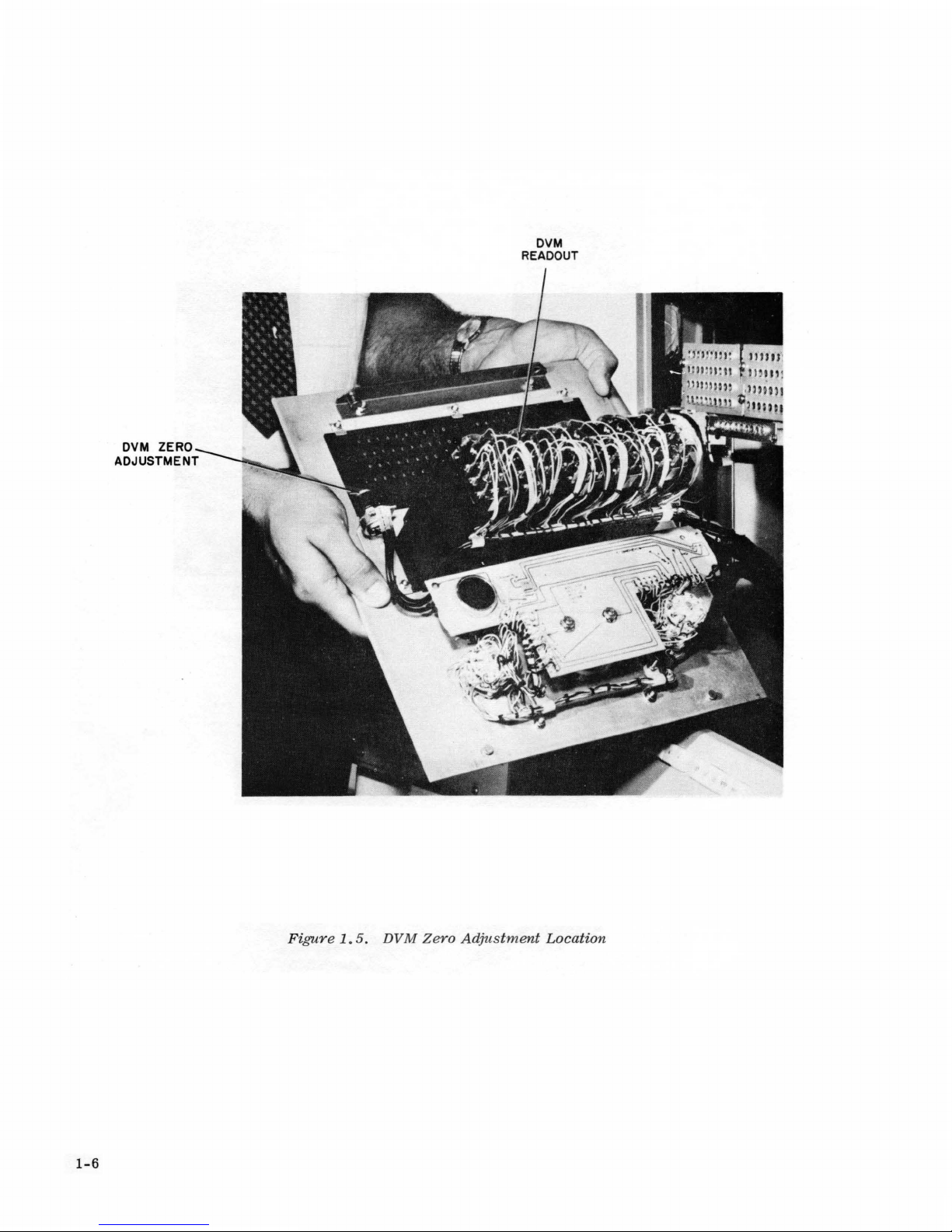
1-6
DVM ZERO
ADJUSTMENT
DVM
READOUT
F
igure
1.5.
DVM Zero
Adjustment
Location
Page 20

1.2.3
To
insert
panel
Push
with
panel
frame
the
the
slightly
matically
patch
panel
position.
Pre-Patch
the
pre-patch
with
pre-patch
slots
on
to
goes
into
drive
the
panel
the
the
the
system
Panel
panel,
slots
top
right.
in
forward
rail
set
pot
faces
Insertion
align
the
bottom
until
of
the
Depress
mode when
the
pre-patch
the
the
patch
the
and
lugs
rail
ENG
Removal
on
of
lugs
bay.
switch.
the
ENG
panel
the
the
on
Gently
switch
bottom
patch
the
to
top
(The
the
of
bay
of
the
slide
computer
is
depressed.)
right
the
pre-patch
(Figure
frame
the
pre-patch
into
1.6).
mate
auto-
the
The
locked
Depressing
patch
panel
1.2.4
'For
accurate
amplifier
input
ment
the
not
this
voltages
in
effect
require
condition
adjustment
the
must
mind,
of
is
DIS
pushbutton
to
the
left
Amplifier
computation,
produce a zero
or
the
the
amplifiers
component
balancing
periodically;
required.
1.
Allow
FUNCTION
pushbutton
2.
Use
output
proceed
ister
meter
3.
If
an
should
located
amplifiers
reading
for
removal.
Balance
the
absence
drift.
for
several
The
a warm-up
switch
the
signal
of
each
in
a
deflection
scale.
amplifier
be
balanced.
behind
on
disengages
operational
output
of
input
contain
Under
weeks.
if
an
amplifier
amplifier
of
in
of
the
MODE
selector
amplifier
order.
causes a larger
the
(Figure
the
voltmeter.
the
amplifier
voltage
voltages
chopper
normal
However,
balance
15
to
30
the
ABAL
switch.
system
to
In
each
that
is
The
balance
pre-patch
1.7).
locking
system
must
when
the
demand
stabilization
circumstances,
it
is
found
is
checked
minutes.
position
to
connect
the
voltmeter.
case,
less
the
than
deflection,
controls
panel
Adjust
on
these
and
remain
combined
it.
With
circuits
the
is
desirable
to
be
unbalanced,
as
Place
and
depress
the
voltmeter
1/2.
division
for
the
front
controls
forces
balanced.
effects
this
amplifiers
follows:
the
voltmeter
stabilizer
Select
should
the
amplifier
amplifiers
block
for a zero
,require-
to
to
the
AOO
on
the
pre-
The
of
the
minimize
do
check
an
SP
and
reg-
the
are
of
the
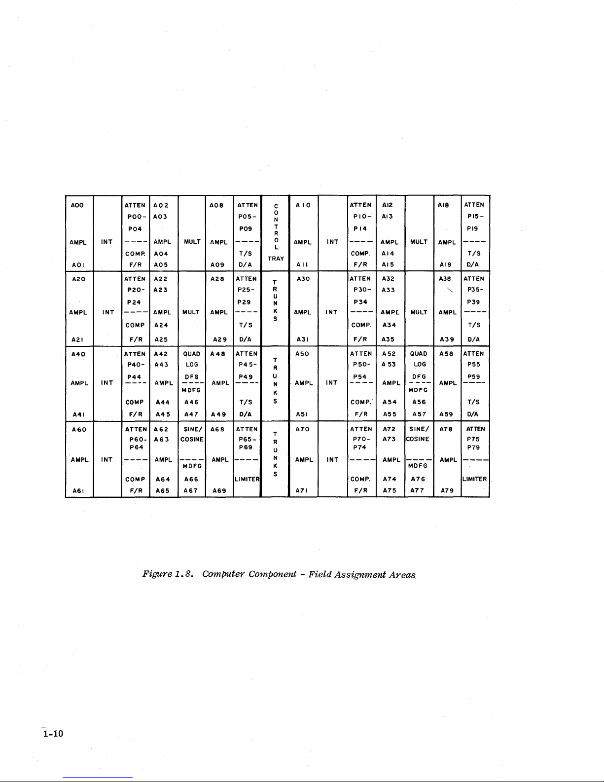
1.2.5
In
the
solution
ponent
signed
to
to
required
in
its
place.
component
component
computing
in
the
following
Changing
of
the
existing
handle
in
the
problem
Figure
in
the
is
compatible
component
some
more
580
field
and
paragraphs.
Computational
problems,
complement.
than
one
type
investigation
1.8
illustrates
area.
with
each
changing
Components
it
may
Since
of
may
the
The
diagram
position.
the
pre-patch
be
necessary
some
computing
be
removed
various
shows
The
to
add a computing
of
the
module
positions
component, a component
and
positions
which
procedure
panel
another
type
for
patching
of
the
of
replacing
block
unit
com-
are
not
inserted
computing
computing
a
is
described
de-
1-7
Page 21

Figure
1.
6.
Pre-Patch
Panel
Insertion
1-8
Page 22
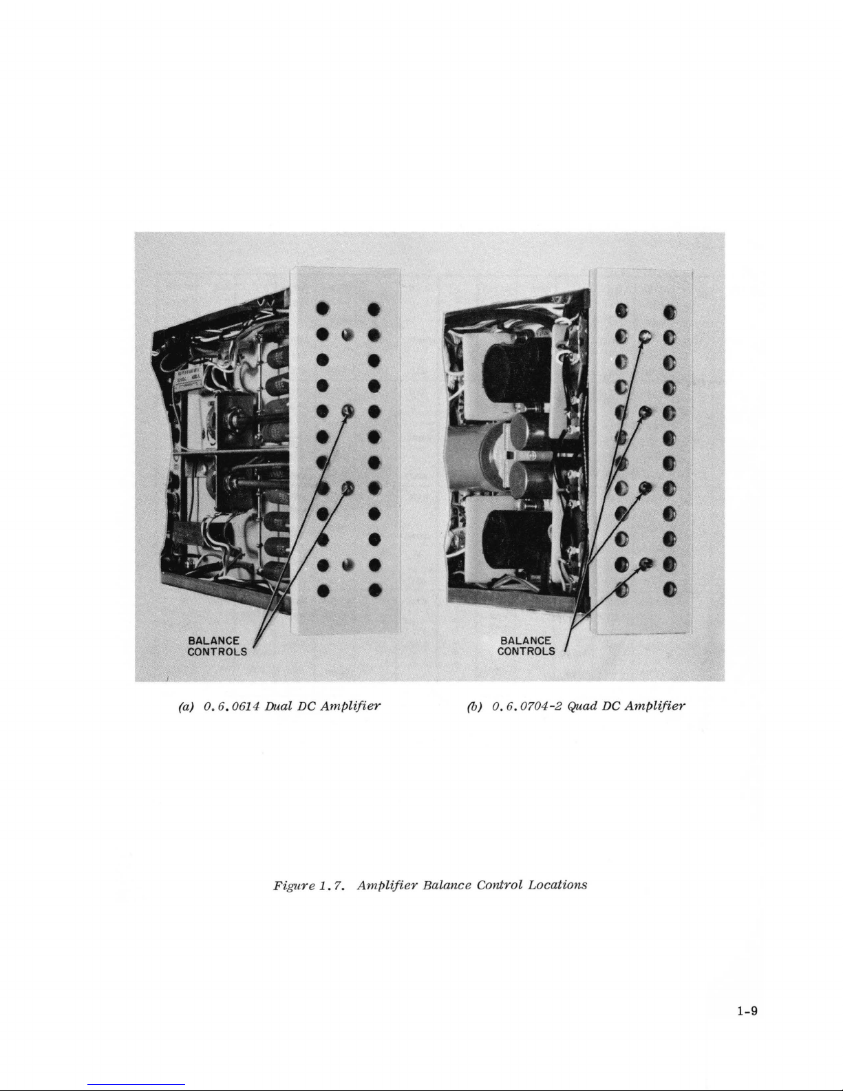
BALANCE
CONTROLS
• •
•••
• •
•
•
•
•
•
•
•
•
•
(a)
0.6
. 0614 Dual DC Ampl
ifier
BALANCE
CONTROLS
(b) 0. 6. 0704-2 Quad DC
Am
plifi
er
F
igure
1.
7.
Amplifier
Balance
Control
Locations
1-9
Page 23
AOO
AMPL
AOI
A20
AMPL
A21
A40
AMPL
A41
A60
AMPL
A61
INT
INT
INT
INT
ATTEN
A02
POO- A03
P04
AMPL
----
COMPo
FIR
ATTEN
A23
P20P24
----
AMPL
COMP
FIR A25
ATTEN
P40P44
----
COMP
FIR
ATTEN
A62
P60P64
----
COMP
FIR A65
A08
MULT
AMPL
A04
A05 A09
A22 A28
MULT
AMPL
A24
A29
QUAD
A42
A43
AMPL
A44
A45
A63
AMPL
A64
COSINE
----
A48
LOG
DFG
----
MDFG
AMPL
A46
A47
A49
SINEI A68
AMPL
MDFG
A66
A67
A69
ATTEN
P05-
P09
----
TIS
D/A
ATTEN
P25-
P29
----
TIS
D/A
ATTEN
P45P49
----
TIS
O/A
ATTEN
P65P69
----
LIMITER
C
0
N
T
R
0
L
TRAY
T
R
U
N
K
S
T
R
U
N
K
S
T
R
U
N
K
S
AIO
AMPL
A
II
A30
AMPL
A31
A50
AMPL
A51
A70
AMPL
A71
INT
INT
INT
INT
ATTEN
PIOPI4
----
COMPo
FIR
ATTEN
P30P34
----
COMPo
FIR
ATTEN
P50-
P54
----
COMPo
FIR A55
AT
TEN
P70-
P74
----
COMPo
FIR
AI2
AI3
AMPL
AI4
AI5 AI9
A32
A33
AMPl
A34
A35
A52
A 53
AMPL
A54
A72
COSINE
A73
AMPL
----
A74
A75 A77
Ale
MULT
AMPL
A38
MULT
AMPL
A39
QUAD
AS8
LOG
DFG
----
MOFG
SINEI A78
MDFG
A56
A57
A76
AMPL
A59
AMPL
A79
"'--
ATTEN
P15-
PI9
----
TIS
D/A
ATTEN
P35-
P39
----
TIS
D/A
ATTEN
P55
P59
----
TIS
D/A
AT
TEN
P75
P79
----
LIMITER
Figure
1.8.
Computer Component - Field
1-10
Assignment
Areas.
Page 24
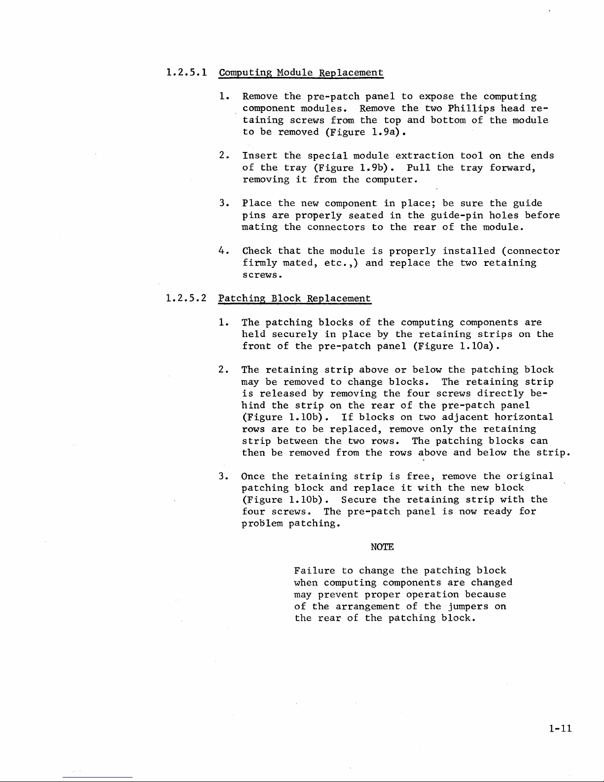
1.2.5.1
Computing
1.
Remove
component
taining
to
be
2.
Insert
of
the
removing
3.
Place
pins
mating
4.
Check
firmly
screws.
Module
the
pre-patch
modules.
screws
removed
the
special
tray
the
are
the
that
(Figure
it
from
new component
properly
connectors
the
mated,
Replacement
panel
Remove
from
the
(Figure
1.9a).
module
1.9b).
the
computer.
seated
to
module
etc.,)
is
and
to
the
top
and
extraction
Pull
in
place;
in
the
the
rear
properly
replace
expose
two
Phillips
bottom
the
be
guide-pin
of
installed
the
the
of
tool
tray
sure
the
two
computing
head
the
module
on
the
forward,
the
guide
holes
before
module.
(connector
retaining
re-
ends
1.2.5.2
Patching
1.
The
held
front
2.
The
may
is
hind
(Figure
rows
strip
then
3.
Once
patching
(Figure
four
problem
Block
patching
securely
of
retaining
be
removed
released
the
1.lOb).
are
between
be
removed
the
1.10b).
screws.
patching.
Failure
when
may
Replacement
blocks
in
the
pre-patch
strip
to
by
removing
strip
to
on
be
replaced,
the
from
retaining
block
and
The
computing
prevent
of
the
arrangement
the
rear
of
place
above
change
the
rear
If
blocks
two
rows.
the
strip
replace
Secure
pre-patch
NOTE
to
change
proper
of
the
the
computing
by
the
retaining
panel
or
(Figure
below
blocks.
the
four
of
the
on
two
remove
The
rows
above
is
free,
it
with
the
retaining
panel
the
components
operation
of
patching
components
1.IOa).
the
The
screws
pre-patch
adjacent
only
the
patching
and
remove
the
is
now
patching
are
the
jumpers
block.
strips
patching
retaining
directly
panel
horizontal
retaining
blocks
below
the
new
block
strip
with
ready
block
changed
because
on
are
on
the
block
strip
be-
can
the
strip.
original
the
for
1-11
Page 25
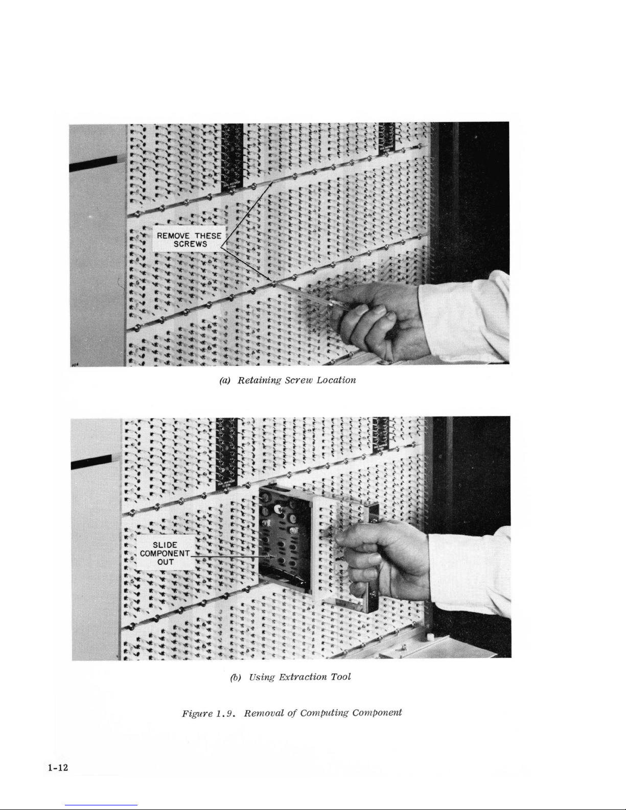
(a)
Retaining Screw
Location
(b) Using
Extraction
Tool
Figure
1.
9.
R
emoval
of
Computing
Component
1-12
Page 26

(a)
Removal
(b)
Replacement
Figure
1.10.
Patching
Block
Replacement
1-13
Page 27

1.3
KEYBOARD
PANEL
1.3.1
The
focal
1.11),
scribe
point
located
the
1.3.2
The
ADDRESS
(Figure
select
1.11).
the
Potentiometer.
in
this
row. The
respectively.
button
field
0
in
the
is
1.3.3
The
RDAC
switches
column
precise
The CL/SET
RDAC
labeled
voltage
pushbuttons
pushbuttons
General
for
to
function
ADDRESS
switch
The
type
of
Table
Note
10 column
to
be
read
Servo
Switches,
0
through
for
have
control
the
left
and
Switch
consists
first
unit
1.1
second
that
out,
Set
consist
automatic
are
been
facilities
of
the
MDFG
,use
of
the
of
three
row,
consisting
to
be
read
identifies
and
third
if
the
position
must
be
depressed.
it
has
Potentiometer
and
the
of 4 columns
9.
The
purpose
setting
used
to
activated.
various
vertical
out,
and
rows
to
be
POT
of
clear
of
the
drawers.
controls
of
seven
i.e.,
describes
contain
selected
For
addressed
Controls
CONTROL)
of
10
pushbutton
of
these
the
Servo
or
to
580
is
The
and
rows
of
pushbuttons,
A
equals
the
the
tens
is
example,
as
(Including
switches
set
~
an
the
keyboard
following
components.
pushbutton
Amplifier,
function
and
units
less
than
if
amplifier
A04.
RDAC
switches
is
to
potentiometers.
addressed
panel
paragraphs
switches
is
used
P
equals
of
each
switches
10,
the ° push-
4
Switches,
with
each
provide
pot
once
(Figure
de-
to
switch
in
CL/SET
a
the
The
POT
CONTROL
As
an
example
particular
Select
Set
the
the
RDAC
pot
pot
to 8 volts
the 0 pushbutton
been
voltage.
address
The
ating
pushbuttons
set,
depress
If
the
1.3.4
ANALOG
modes
it
pot
ANALOG
MODE
and
associated
1.3,5
The
PATCH
when
PANEL
inserting
lever
of
the
is
to
to
be
in
the
is
and
controls
the
PATCH
DIS/ENG
or
removing
allows
operation
be
set
set
using
by
the
second,
SET
button
necessary
change
MODE
are,
computer
with
PANEL
switches
adjustment
of
to 8 volts.
the
depressing
third
to
change
the
value
Controls
divided
set-up
these
DIS/ENG
the
pre-patch
the
controls
selector
the 8 pushbutton
and
and
the
up
in
modes.
modes
Switches
provide
of
an
Place
system
fourth
addressed
the
value
or
down
two
types
Tables
and
describes
control
panel
addressed
described
the
computer
described
columns.
pot
of a pot
using
of
modes;
1.2
of
the
(see
Paragraph
pot
above,
in
will
the
and
their
patch
in
any
in
the
in
the
first
Once
slew
during
POT
CONTROL
the
1.3
indicate
functions.
panel
1.2.3).
computer
assume
~
E2l mode.
that
Paragraph
column
the
RDAC
to
the
problem
lever.
computer
drive
mode.
a
1.3.1.
and
has
proper
solution,
oper-
the
system
1-14
Page 28

Figure
1.
11.
Keyboard
1-15
Page 29

Table
1.1
Pushbutton
DIG
I/O
PP
F
D
D/lO
P
Depressing
readout
the
This
terminal
selection
580
is
pushbutton
on
input.
Depressing
button
lower
0.12.1345
on
MDFG
MDFG
the
DVM.
pushbutton
This
the
summing
units.
Same
as
the D (derivative)
voltage
The P
readout
(potentiometer)
potentiometer
this
pushbutton
installed
is
the
0812.1607
this
pushbutton
Amplifier
drawer,
Amplifier
is
junctions
is
addressed
Function
system
in a hybrid
used
to
Balance
allows
used
for a derivative
of
divided
pushbutton
to
transfers
to a digital
configuration.
connect
Control
and
Tray
the
Panel,
the
amplifiers,
Network,
the
to
integrators
pushbutton
by a factor
connects
the
DVM.
control
computer
the
DVM
patch
to
the
appropriate
located
located
be
ba
lanced
readout
and
except
of
10.
the
of
the
when
DVM
push-
in
the
in
'on
the
from
.track/store
that
arm
in
of
the
the
A
Mode
OPERATE
(Q£)
HOLD
(1m)
INITIAL
DITION (1£)
REMOTE
CON-
(RMT)
The A
output
to
Table
1.2.
Integrators
to a patched
Integrators
the
hold
Integrators
Parallels
(amplifier)
of
the
DVM
Definitions
operate;
problem.
do
mode
is
are
mode
the
selected
input.
not
operate;
selected
set
control
pushbutton
of
Computer
Function
computer
to
initial
of
amplifier
produces
all
values
are
returned.
values.
computer
when
depressed
or
MDFG
Operating
a
present
to
external
setup
Modes
dynamic
at
switches
amplifier
solution
the
devices.
the
time
1-16
Page 30

Table
1.3.
Definition
of
Computer
Set-Up
Modes
Mode
STATIC
(21)
SET
POT
<g)
PROGRAM
<W
1.3.6
The
TIME
trol
the
generates
the
computer
p~ovide
a 500
TEST
PANEL
SCALE
analog
the
for
Similar
be
applied
tial
condition
levels
All
INT
All
amplifiers
provide
applied
that
the
plifier
mitting
When
this
modes may
0.12.1607
the
internal
TIME
SCALE
Switches
and X switches
timer
precise
(repetitive
time
iterative
to 1 speed-up
to
initial
to
at
other
and
correct
to
high
pot
is
connected
the
button
be
Control
intervals
or
of
integrators
voltages,
parts
TIs
are
provided
attenuator
end
coefficient
pot
to
is
controlled
Tray
timer
and
along
with
operation)
necessary
repetitive
the
entire
Function
condition.
not
of
the
forced
with
of
any
may
to
the
be
set.
depressed
by
patch
to
automatically
Controls
the
operation.
computer.
Static
normally
to
permit
program
to
IC mode.
low
loading.
pot
selected
be
read
motor
the
logic
block.
TIMER
circuit.
to
control
test
provided
checking
via
impedance
Reference
for
out.
of
an
addressed
IC,
HOLD,
signals
This
start
controls
The
the
The
TIME
voltages
computed
Function
feedback
voltage
readout,
The
servo
and
applied
mode
also
operation.
are
used
timer
circuit
analog
SCALE
can
with
ini-
Relays.
to
so
am-
pot,
OPERATE
to
the
causes
to
con-
modes
pushbuttons
per-
of
The
repetitive
repetitive
selected
between
ment
The
of
timer
terminates
starts
condition
the
analog
may
be
When
When
A
RUN = 0,
RUN
(rC)
and A as
operation.
by
the
pushbutton
the A (IC)
has
the
1.3.6.1
in
the
and
stops
other
simulation
patched
the
becomes
period,
long
as
operation
pushbuttons
settings.
and
following
control
the
than
(Rep-Op)
Any
A (OP)
Input.
tray
timer,
elapsed
until
OPERATE
and
Separate
periods.
inputs,
The
and
time.
some
from a comparator.
timer
high
followed
does
(logic
by
not
ONE)
anA
RUN = 1.
circuit
or
Vernier
"RUN"
in
the
allows
analog
run;
the
(OP)
IC
period
controls
Vernier
outputs,
tenninal
center
rep-op
For
example,
variable
its
timer
period.
allows
and
of
runs
output
starts
It
both
from 100
provided
controls
controls:
on
the
the
first
to
if
it
crosses
remains
to
continues
high-speed,
~sec
are
to
to
"bridge
provided
analog
row.
be
terminated
is
desired
zero,
in
the A (IC)
run,
starting
to
cycle
100
patch
This
the
and
to
RUN
low-speed
sec
may
be
the
gap"
for
adjust-
panel
input
by some
operate
input
state.
with a full
between
A
1-17
Page 31

In
ordinary
by
the
connected
labeled
no
special
periods,
control
terminal
repetitive
operator,
to
the
"pp"
(Paragraph
patching;
and
depresses
the
timer
overrides
there
"PP"
from
the
operation,
is
no
signal,
1.3.3).
the
operator
the
an
arbitrary
internal
need
which
"PP"
where
to
Thus,
the
patch
is
controlled
ordinary
simply
button.
logic
connection.
OPERATE
the
RUN
selects
However,
signal,
period
input.
by
the
repetitive
the
desired
if
the
local
is
It
ANALOG
operation
A
operator
patching
fixed
is
internally
MODE
(IC)
desired
at
in
advance
button
requires
and
A (OP)
the
RUN
to
an
analog
Control
spectively.
A
terminals,
terminals
trol
of
The
TB
output
a
voltage
zontal
used
axis
as
The ramp
cycle.
Thus,
operate
which
sets
means
of
controls:
(multiplier)
1
sec).
timer
well
only,
as
1.3.6.2
output
Tray.
The A and A outputs
The
act
override
the
IC
and
is
proportional
of
readout
an
analog
integrates
the
cycle.
(tit
1.3.6.3
pushbuttons
Note
that
while
the
capacitors
TB
IC
as
OP
an
signal
scaled
(This
) =
max.
a
the
the
Outputs.
(Time
and
inputs
the
internally
buses.
analog
to
devices
from
is a unit
1.0
Controls.
pair
dials
TIME
in
Base).
OP
patch
ramp
time.
for
zero
output
unit,
of
(.1,
the
to
the
(Plotting
problems
to
dials
1,
and
SCALE
computer
The
timer
The
terminals
normally
terminals,
IC
and
generated
generated
The ramp
requiring
plus
is
scaled
or
(tit
10
The
reference
max max
notation;
volts.)
period
(one
10),
and
the
multiplier
pushbuttons
has
two
control
connected
OP
buses.
signals
by
an
output
Board,
),
where
of
for
A,
two
TIME
control
integrators.
logic
are
outputs
connected
the
IC
internally
Logic
and
provide
internal
may
be
integrator
used
Oscilloscope,
a
signal
voltage
t
the
the
one
SCALE
proportional
during a given
is
run
terminates
timer
for
A), a
pushbuttons
pushbuttons
the
to
and
OP
signals
to
etc.,)
the
length
is
determined
group
affect
timer
(A
and
the
0.12.1607
buses
to
the A and
at
these
external
and
drive
the
or
to
operate
of
when t = t
of
three
(2
the
rep-op
integrator
A)
and
re-
con-
provides
hori-
may
be
time.
the
by
three
X
msec,
as
max'
The A
A window
complete
fractional
set
Consequently
10.5
The
in
selected
The
of
A
TIME
the
and X controls
at
the
revolutions
part
for
5.20
turns,
the
turns.
multiplier
such a manner
pushbutton.
length
turns
simple
of
the A and X periods
on
the
equation
SCALE X Multiplier
minimum
and
utilize
top
of
of
of a revolution
8.75
minimum
pushbuttons
that
when
Vernier
for
determining
maximum
1-18
each
the
dial
dial~
turns,
position
are a series
one
dial,
X
Vernier
time
periods
ten-turn
displays
to
etc.
is
is
depressed
is
the
multiplier
the
=
Vernier
The
graduations
be
set
The
0.50
the
lengths
Length
for
an
to
dial
turns
of
momentary
it
product
of
each
dials
integer
around
two
figures.
has
been
while
electrically
of
setting,
of
either
Period.
range.
with a built-in
representing
the
dial
Thus,
offset
the
maximum
contact
by
switches
clears
three
and
factors:
the
TIME
the A or A periods
The
following
turn
the
allows
the
dial
0.50
position
any
the
SCALE
table
counter.
number
of
a
can
turns.
is
connected
previously
number
selected.
is
gives
be
Page 32

A 500
to I speedup
pushbuttons.
in
each
integrator
up
controls
time
scale
gizing
problem
up
high
normal
this
by a factor
by a factor
(+5v)
problem
The
both
bus
relay
logic
of
TIME
tray
integrators
is
at a logic
switches
of
of
500.)
level,
speed.
the
SCALE
through
500.
The 1
the
entire
computer
pushbuttons
the
in a dual
ZERO
capacitance
(The
SEC
relays
control
time
integrator
level
energizing
from
problem
pushbutton
are
de-energized
is
also
scale
bus
10
~f
is
automatically
switches
provided
the
time
system.
tray.
the
to
0.02
and
In
time
the
the
by
the
scale
The 500
the 2 ms
scale
~f,
speeding
rescaled
time
computer
TIME
relays
to 1 speed-
relay.
when
scale
SCALE
located
range,
Ener-
up
the
speeded
bus
to
resumes
the
a
Note
By
that
local
grators,
selection
a
factor
TIME
2
2
2Ms
1
1
1
1.3.7
the
patching,
located
system.
of
SCALE
MS
MS
SEC
SEC
SEC
TIME
SCALE
it
in a particular
In
10
to 1 individual
(Multiplier)
XlO.O
XlO.O
POWER
Pushbuttons
pushbuttons
is
possible
addition,
Table
X
XO.l
XI.O
XO.l
Xl.O
only
to
control
tray,
it
independent
is
possible,
integrators.
1.4.
Vernier
0.5
0.5
0.5
0.5
0.5
0.5
t
affect
Time
to
to
10.5
to
10.5
to
10.5
to
10.5
to
10.5
the
Periods
10.5
the
time
by
normally
scale
of
the
local
100
1
10
50
0.5
5.0
input
master
patching,
Time
to
\-LS
to
MS
to
MS
to
MS
to
Sec
to
Sec
patched
of
time
to
2
MS
20
MS
200
MS
1.0
SEC
10.0
100.0
integrators.
the
intescale
speed
SEC
SEC
up
The
POWER
the
computer,
the
OFF
to
indicate
The
LOGIC
to
control
manner
modes.
selected.
installed
LOGIC
pushbuttons
pushbutton.
1.3.8
MODE
the
that
when
An
indicator
The
in
MODE
pushbutton.
depress
that
the
LOGIC
pushbuttons
580
one
LOGIC
the
computer.
MODE
Logic
MODE
control
the
ON
The
ON
computer
Pushbuttons
consist
Package.
is
depressed
lamp
in
pushbuttons
the
power
pushbutton.
pushbutton
is
"ON".
of
These
it
each
pushbutton
Table
1.5
for
the
To
turn
contains
four
momentary
switches
electrically
indicates,
are
included
lists
the
entire
an
computer.
the
computer
indicator
pushbutton
are
connected
clears
when
only
when a
description
any
and
To
off,
lamp
depress
which
switches
in
such
previously
lit,
which
logic
function
activate
lights
used
a
selected
mode
package
of
is
is
each
1-19
Page 33
Table
1.5.
LOGIC
MODES
LOGIC
PP
(Patch
C
(Clear)
S
(Stop)
R (Run)
1.3.9
The
four
for
the
synchronized
momentary
electrically
pushbuttons
Table
1.6
MODE
Panel)
clock
contact
clear
include
lists
Logic
rate
the
Transfers
Clears
those
mains
Stops
isters
devices
Normally
flops,
Clock
pushbuttons
logic
switches
the
previously
lamps
function
all
in
high
the
from
may
registers)
Rate
Pushbuttons
elements
which,
which
of
control
flip-flops
the
counters
preventing
logic
reacting
still
used
(10
for
6 5
, 10 ,
in
when
selected
indicate
each
clock
Function
of
logic
in
and
initialization.)
clock
preventing
to
set
and
computation.
respond
10,
the
logic
depressed,
clock
which
rate
mode
the
logic
registers.
patched
reset
to
patch
and
STEP)
package.
select
rate.
clock
rate
pushbutton.
to
the
logic
package
(Clear
flip-flops
inputs.
(Clocked
manually.)
Clocked
select
a
devices
panel
inputs.
the
The
pushbuttons
new6cloc~
The 10 , 10 ,
has
been
patch
panel.
including
line
re-
and
reg-
(flip-
clock
rate
are
rate
and
and
10
sele~ted.
Clock
10
STEP
1.3.10
The
RMT
logic
source
mode
may
Computer
Rate
Logic
(remote)
control
be a digital
when two
Table
Considered
second.
One
clock
Ten
clock
Inhibits
one-clock
RMT
(Remote)
pushbutton
and
clock
computer
or
more
1.6.
Clock
normal
pulse
every
pulses
all
clock
pulse
when
Pushbutton
is a latching
rate
control
in a hybrid
are
connected
Rate
clock
10
every
pulses
subsequently
in a slaved
Pushbutton
Function
rate.
One
microseconds.
second.
when
type
initially
pushbutton
with a remote
configuration
Functions
clock
pulse
depressed.
depressed.
which
source.
or
another
configuration.
every
parallels
The
remote
580
micro-
Provides
both
1-20
Page 34

1.4
The
a
this
following
components.
THE
analog
multi-range
panel
ANALOG
readout
if a digital
paragraphs
READOUT
panel
VOLTMETER. A DIGITAL
PANEL
(Figure
voltmeter
describe
the
1.12)
consists
VOLTMETER
(DVM)
function
is
provided
and
of
amplifier
readout
use
of
display
with
the
OVERLOAD
the
computer.
various
is
also
controls
indicators,
located
The
and
on
1.4.1
The
amplifier
individual
with
The
The
The
are:
position
meter.
each
normally
fier
is
lamps
have
overrange.
selected
from
represents
equivalent
directly
may
settled
1.4.2
DVM
±O.OOOO
1.4.3
VOLTMETER
RANGE
30,
Amplifier
OVERLOAD
amplifier.
amplifier
extinguished.
in
an
overload
light
readout
potentiometer
below
switch
10,
is
but
down.
The DIGITAL
displays
The
output
to
±1.1999
the
voltage
to
11.999
The
is
controlled
the
selects
3,
1,
also
provided
OVERLOAD
indicators
The
position
A
lit
condition.
should
volts
VOLTMETER
meter.
3,
be
VOLTMETER
four
of
any
can
be
which,
into
the
and
0.1
on
Indicators
provide a graphic
indicators
in
the
position
extinguished
digits,
selected
displayed
when
the
DVM.
(UNITS
by
DISPLAYED X REFERENCE
the
voltage
volt
this
switch
are
computer.
indicates
During
(DVM)
mUltiplied
RANGE
for
a
polarity
amplifier
on
As
an
and
range
full
to
warm-up
overload
numbered
once
•
Readout
the
example a reading
FUNCTION
of
the
scale
convert
The
that
periods,
the
sign,
in
DVM.
with
meter.
(AOO
overload
the
corresponding
and a fifth
the
The
the
rotary
meter
the
display
to
A79)
corresponding
various
coefficient
reading
reference
VOLTAGE).
- The
deflection.
VOLTMETER
to
indicators
may
of
1.1999
switches
ranges
for
correspond
are
ampli-
overload
amplifiers
digit
of
any
range
voltage,
is
located
provided
A
NULL
to a null
each
for
The
FUNCTION
positions
these
to
RANGE
1.5
The
indicators
the
A
eight
positions
ensure
switch
THE
auxiliary
ten
1.5.1
pair
comparators
handset
of
switch
on
the
switch
enable
proper
AUXILIARY
for
pushbuttons
computer
position.
control
the
pots
The
COMPARATOR
in
determines
CONTROL
interface
are
the
panel
(PO
(one
the
the
primarily
operator
operation.
PANEL
(Figure
components
through
Controls
numbered,
computer.
source
P9).
used
to
quickly
Table
1.13)
(comparator
one
These
of
the
for
maintenance
check
1.7
describes
contains
blank)
pushbuttons
is
input
all
the
and
provided
signal.
purposes.
power
the
pushbutton
function
for
are
used
Note
supply
function
controls
relays),
each
to
force
that
many
However,
voltages
of
each
and
and
of
the
the
1-21
Page 35
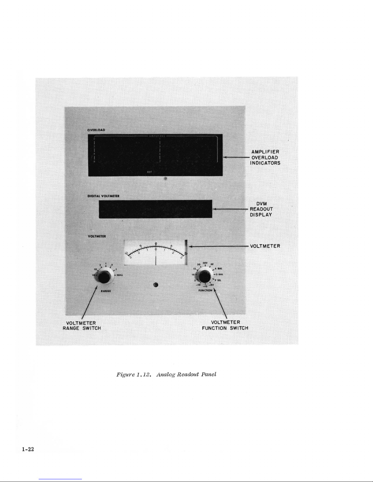
1-22
VOLTMETER
RANGE SWITCH
AMPLIFIER
""""--.--
OVERLOAD
INDICATORS
DVM
,--.-----....,..
READOUT
DISPLAY
~~----------~-VOLTMETER
-
-\
0/,-
- ' ",.:
VOLTMETER
FUNCTION SWITCH
Fi
gure
1.1
2 .
Analog
Readout Panel
Page 36
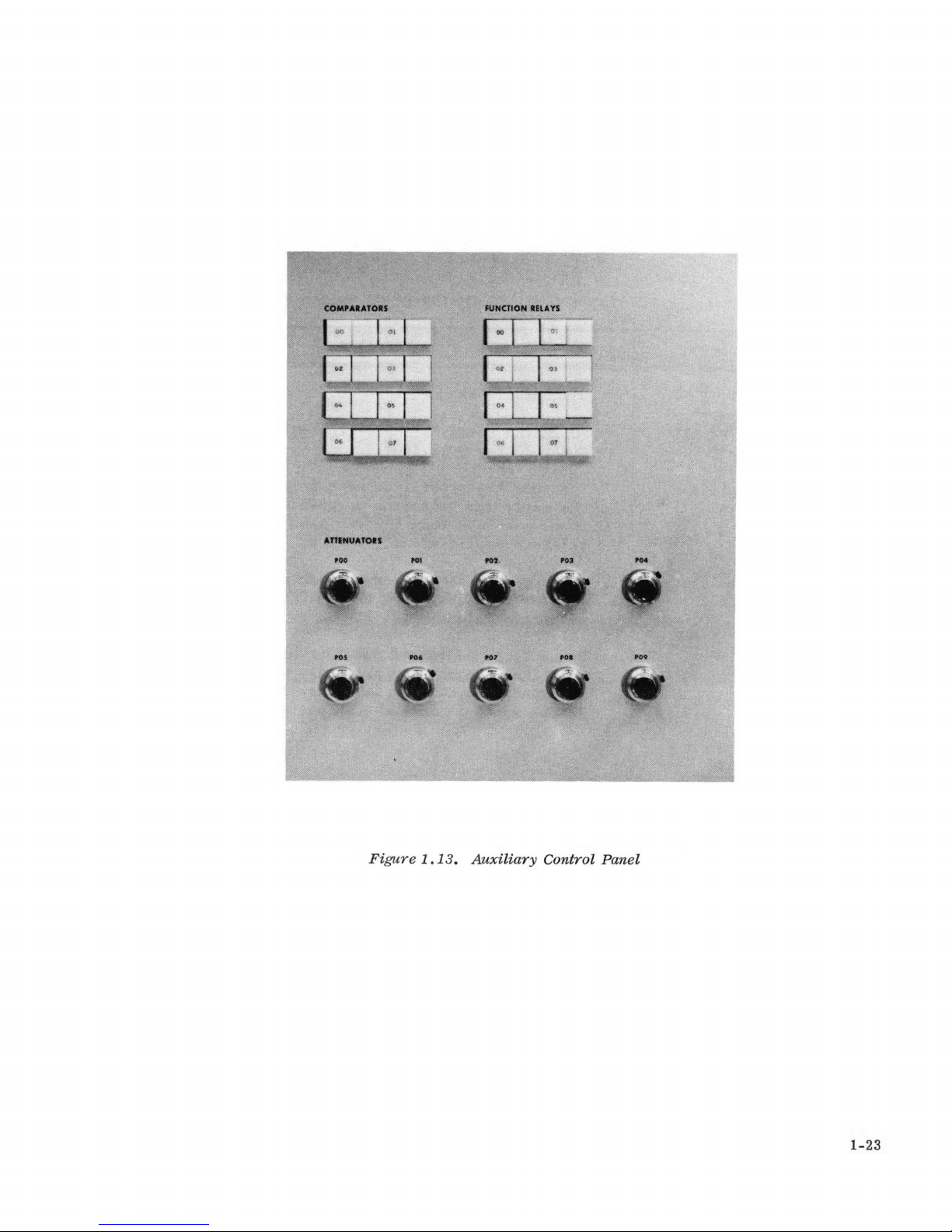
COMPAlAto.S
FUNCTION
.llA
YS
...
'"
-
POt
- -
'"
-
Figure
1
.13.
Auxiliary
Control Panel
1-23
Page 37
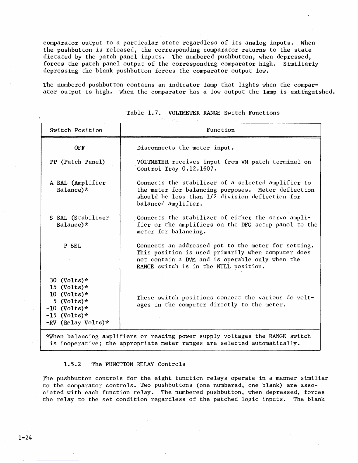
comparator
the
pushbutton
dictated
forces
depressing
The
ator
the
numbered
output
output
by
the
patch
the
pushbutton
is
to a particular
is
released,
patch
panel
blank
high.
panel
output
pushbutton
When
the
inputs.
contains
the
state
corresponding
The
of
the
corresponding
forces
an
indicator
comparator
regardless
numbered
the
comparator
has
of
its
comparator
pushbutton,
comparator
output
lamp
a low
that
output
analog
returns
lights
the
when
high.
low.
when
lamp
inputs.
to
the
depressed,
Similiarly
the
is
When
state
compar-
extinguished.
Switch
PP
(Patch
A
BAL
Balance)
S
BAL
Balance)*
30
(Volts)*
15
(Volts)*
10
(Volts)*
5
(Volts)*
-10
(Volts)*
-15
(Volts)*
-RV
(Relay
Position
OFF
(Amplifier
(Stabilizer
P
SEL
Panel)
*
Volts)*
Table
1.7.
Disconnects
VOLTMETER
Control
Connects
the
should
balanced
Connects
fier
meter
Connects
This
not
RANGE
These
ages
VOLTMETER
Tray
meter
be
amplifier.
or
the
for
an
position
contain
switch
switch
in
the
the
meter
receives
0.12.1607.
the
stabilizer
for
balancing
less
than
the
stabilizer
amplifiers
balancing.
addressed
is
a
DVM
is
positions
computer
used
and
in
RANGE
Function
input.
input
of a selected
purposes.
1/2
division
of
on
pot
primarily
is
the
NULL
connect
directly
Switch
from
VM
either
the
DFG
to
the
operable
position.
the
to
Functions
patch
amplifier
Meter
deflection
the
servo
setup
meter
when
only
various
the
computer
meter.
terminal
deflection
for
ampli-
panel
for
setting.
when
the
dc
on
to
to
does
volt-
the
*When
The
to
ciated
the
balancing
is
inoperative;
1.5.2
pushbutton
the
comparator
with
relay
to
The
each
the
amplifiers
the
FUNCTION
controls
controls.
function
set
appropriate
condition
1-24
for
or
RELAY
the
Two
relay.
reading
meter
Controls
eight
pushbuttons
regardless
The
function
numbered
power
ranges
of
supply
are
relays
(one
numbered,
pushbutton,
the
patched
voltages
selected
operate
the
RANGE
automatically.
in a manner
one
blank)
when
logic
depressed,
inputs.
switch
are
The
similiar
asso-
forces
blank
Page 38
pushbutton,
the
function
the
patch
pushbuttons.
function
ciated
pushbuttons.
1.5.3
Ten
handset
Each
manner
ATTENUATOR
similar
justed.
.
device.
using
the
when
depressed,
relay
panel
inputs
Consequently,
relay
can
The
ATTENUATORS
is
to
Set
each
If
the
computer
nulling
resets
returns
are
to
not
with
be
used
Handset
as a manual
ATTENUATORS
(POO
addressable
the
servo
set
ATTENUATOR
does
method
on
the
the
the
state
patched
no
to
P09)
on
the
attenuators
to
the
not
contain
VOLTMETER.
relay.
dictated
they
logic
function
are
provided
signal
desired
remain
signals
selector
except
value
a
DVM,
When
by
switch
on
the
the
pushbutton
the
patch
in
the
state
patched
to
controlled
the
auxiliary
system
that
they
using
the
ATTENUATORS
panel
selected
its
inputs,
by
control
and
is
are
manually
DVM
as a readout
have
is
released,
inputs.
its
set
to
by
the
asso-
panel.
in
ad-
be
If
the
a
set
1.6
The
left
AND
THE
logic
of
gate
dicators
BUTTONS
various
paragraphs.
1.6.1
The
digital
and
outputs
patch
(0
panel
through
particular
with
their
1.6.2
The
AND
gate
AND
gate.
dicator
is
laid
is
out
LOGIC
control
the
analog
indicators,
and
thumbwheel
and
repetitive
controls
The
patch panel
of
is
2).
patching
associated
The
display
When
numbered
in
CONTROL
and
patch
and
Digital
the
logic
divided
Each
of
areas
AND
is
the
indicator
and
the
same
AND
INDICATOR
indicator
panel.
the
REGISTER
controls
operation
indicators
Patc~
(Figure
devices
into
four
the
fields
and
units.
Gate
Display
provided
lettered
configuration
panel
The
indicators
for
TIME
mentioned
Panel
1.15)
in
fields
and
the
patch
to
is
lit,
to
PANEL
(Figure
panel
the
contains
COUNTERS,
controls
above
is
used
the
logic
(0
through
trunk
termination
indicate
the
output
correspond
as
the
1.14)
is
the
and
pushbutton
the
(A
and
A). The
are
described
to
provide
package.
3)
and
areas
are
functions
the
output
of
the
to
the
gates,
terminations
located
digital
controls,
general
access
Physically
three
similar
state
gate
is
and
on
the
at
the
patch
purpose
operation
in
the
to
the
the
trunk
in
layout.
are
described
of
each
high.
in
patch
upper
panel,
the
in-
PUSH-
of
following
inputs
logic
areas
individual
The
addition,
panel.
the
The
in-
The
1.6.3
A
fully
bits
blank
flop.
guished
depressing
dicator
expanded
each
for a total
pushbutton
The
numbered
when
it
but
serves
REGISTER
580
are
cleared.
sets
Computer
provided
pushbutton
the
as a manual
Controls
of
16
The
numbered
flip-flop.
logic
flip-flops.
as
manual
lights
The
clear
and
Indicators
package
contains
A
numbered
controls
when
the
pushbutton
blank
control
pushbutton
and
flip-flop
also
serves
pushbutton
for
its
associated
four
registers
indicator
is
as a manual
is
not
set
of
and
the
for
each
and
is
used
as
flip-flop.
four
adjacent
flipextincontrol;
an
in-
1-25
Page 39

REGISTER CONTROLS
INDICATORS
AND AND
INDICATORS
THUMBWHEEL SWITCHES
FOR
COUNTERS
GENERAL
PURPOSE
PUSHBUTTONS
REP-OP
TIMER
CONTROLS
DIGITAL
PATCH
PANEL
Figure
1.1
4. L
ogic
Cont
rol
and I
ndicator
Pane l
1-26
Page 40

-
I'L,D
1
•••••••••••••••••••••••
Figure
1.15.
Digital
Patch
Panel
•
'i
1-27
Page 41

The
registers
isters
is
are
necessary
considered
are
numbered
numbered
since,
to
be
on
in
the
by
convention,
the
left.
0,
1, 2 and 3 while
reverse
order.
the
most
the
The
reverse
significant
flip-flops
order
bit
within
of
the
the
flip-flops
of a counter
reg-
is
1.6.4
A
fully
be
used
expanded
for
provided
dicator
lamp;
Depressing
the
count
low.
is
output
input
gates
The
loaded).
through
for
can
separate
The
preset
the
left
than
10
(0
The
counter
pressing
1.6.5
The
COUNTER
580
counting
by
pushbuttons
it
lights
pushbutton
reaches
output
00,
stays
Automatic
an
AND
the
patched
be
patched
output
load
functions.
value
thumbwheel.
through
is
reset
the
manual
The
General
Computer
or
timing
S
whenever
S
sets
the
low
loading
gate
AND
to
make
is
simply a matter
represents
9)
the
by
patching
reset
Controls
logic
functions.
(set)
the
output
until
of
(for
gates
the
the
left
thumbwheel
(R)
pushbutton
Purpose
and
Indicators
package
Manual
and R (reset).
the
counter
output
flip-flop
the
the
time
serves
counter
flip-flop
is
output
counter
delay)
as a controlling
operation
of
tens
count.
is
a
high
to
the R (reset)
on
PUSHBUTTONS
contains
control
Pushbutton
output
and
reset,
flip-flop
is
accomplished
to
the S patch
selecting
In
set
to
the
computer
four
counters
of
is
high.
loads
and
the
is
again
input;
dependent
the
proper
the
event
zero.
patch
keyboard.
the
counter
S
contains
the
counter.
counter
set
by
patching
terminal.
that
on
two
count
the
count
·terminal
which
an
out~ut
(the
counter
The
is
the
or
more
while
is
or
may
is
in-
When
goes
the
second
AND
less
de-
The
six
general
are
latching-type
Two
pushbutton
is
used
is
used
an
indicator
When
the
ciated
length)
with
available
1.6.6
The
rep-op
the
corresponding
circuit
1.7
The
temporarily
METER,
voltages.
which
READOUT
problem
discussed
to
set
to
reset
output
TIMER
In
purpose
switches
controls
the
switch
the
switch
which,
when
of a PUSHBUTTON
that
output,
at
the
The
TIMER
controls
mod~s
lights
when
DEVICES
solution
displayed
obtained
on
previously,
repetitive
PUSHBUTTONS
whose
are
(output
outputs
provided·for
is
(output
lit,
generates
output
indicates
is
zero,
a
terminal.
Controls
(A
and
A)
(A = IC,
the
several
timer
with
may
A =
the
types
be
operation,
provided
are
each
high),
low).
and
The
that
depressing
synchronized
are
used
OP).
is
in
The A
the
580 may
of
readout
used
the
to
measure
computer
in
the
580
terminated
switch.
the
adjacent
numbered
the
associated
the
pulse
to
manually
pushbutton
IC mode.
be
permanently
devices.
steady-state
solution
Computer
on
the
The
numbered
pushbutton
pushbutton
output
blank
(one
pushbutton
clock
force
contains
The
is
displayed
logic
patch
panel.
pushbutton
also
is
period
the
timer
an
recorded
DVM
or
computational
package
(blank)
contains
high.
asso-
in
into
indicator
or
VOLT-
on
an
1-28
Page 42

oscilloscope
oscilloscope
strip
chart
display
and a permanent
trace.
recorders,
problem
variables.
Computer by means
1.16)
located
at
of
the
X-Y
such
the
rear
record
plotters,
as
the
These
connectors
of
the
computer.
can
be
such
as
EAI 8875
readout
provided
obtained
the
EAI 1110
RECORDER,
devices
on
the
by
photographing
VARIPLOTTER~,
can
are
connected
connector
also
be
to
panel
the
used
the
(Figure
or
to
580
1-29
Page 43

OSCILLOSCOPE
CONNECTOR
(SCOPE-I)
AT ,
\ii' • •
-
Figure
1.16.
•
Readout Device
......
,
RECORDER
CONNECTOR
(REC-I)
Connectors
j
1-30
Page 44

CHAPTER
2
2.1.
The
The
linear
stant,
INTRODUCTION
operational
amplifier
computations
and
nonlinear
generation
There
are
0.6.614-1
block
layout
resistor
2.2
The
works
The
for
DUAL
input
are
nonlinear
ease
may
inversion.
operations
or
analytic
two
amplifiers
and
Quad
and
network.
DC
AMPLIFIER
and
output
terminated
components
of
patching
amplifier
be
used
such
such
DC
Amplifier,
simplified
terminations
at
and
OPERATIONAL
is
the
in
conjunction
as
summation,
Accessory
as
multiplication
or
arbitrary
used
in
schematic
PATCHING
the
pre-patch
are
also
short
patch
AMPLIFIERS
basic
computing
with
integration,
components
functions.
the
580.
Model
of
6.704-2.
of
each
the
dual
panel
located
cord
appropriate
permit
and
These
amplifier
amplifier
and
in
close
runs.
element
multiplication
use
division
are:Dual
Figure
are
arranged
proximity
in
networks
of
the
of
DC
2.1
type
and
an
analog
by a con-
amplifier
variables,
Amplifier,
shows
dual
and
for
to
the
the
resistor
ease
the
computer.
to
perform
for
and
Model
patch
associated
of
patching.
amplifiers
the
net-
Patching
linear
ing
the
Figure
Model
2.2a)
circuit
of-one
cuit
ally
The
an
components,
to
the
amplifier
2.2
0.6.614-1
makes
shown
and
is
shown
placed
lower
of-one-tenth
programming
e.
Additional
terminations
Resistors
to
obtain
Appendix
1.
amplifier
particular
used
illustrates
Amplifier.
use
of
schematically
two
gain-of-ten
in
in
the
amplifier
inputs
symbol
input
of
different
may
be
desired
for
is
covered
component.
in
conjunction
the
Figure
triangle.
(Figure
using
for
resistors
patched
gains.
use
two
of
The
standard
in
inputs.
2.2c.
2.2a)
two
this
configuration
resistor
in
series
Some
with
in
the
an
separate
This
with a resistor
the
more
patching
4-pin
bottle
Figure
The
Note
that
Normally,
is
patched
2-pin
can
bottle
be
made
networks
or
parallel
of
these
integrator
sections
section
·common
shown
is
patching
for
plug
2.2b.
basic
the
only
This
programming
amplifier
those
for
plugs.
are
illustrated
available
together
in
configurations
network,
limited
of
or
this
to
network.
arrangements
the
upper
and
provides
configuration
symbol
address
inputs
one
gain-of-one
The
by
as
the
to
simplified
connecting
shown
input
are
one
of
manual
the
description
amplifier
the
has
for
number
be
used
and
schematic
in
Figures
in
Figure
or
feedback
summarized
the
non-
pertain-
for
the
(Figure
summing
two
gain-
this
is
are
three
2.2d
the
RJ
2.2f.
circuit
in
of
cirnormshown.
gain-
and
and
2-1
Page 45

(a)
6.
614
and
Simplified
10K
RJ
IF~O
10K
10
SET
RELAY BUS
-1 Dual DC
Schematic
lOOK
I
I
POT
~SET
KI
Amplifier
POT
Palch
Block
(One Channel)
2-2
NOTES
:
L
SET
POT
RELAYS
SHOWN
IN
DE-ENER
2. DUAL AMPLIFIERS HAVE t SET
HAVE 2 SET POT
RELAYS EACH.
GIZED CONDITION .
POT
RELAY
F
(Patch
I.~IOK
10
EACH . QUAD
igure
AMPLIFIERS
2.1.
Block Layout
~
10K
(b) 6.
704-2
Quad DC
and
Simplified
580 Operationnl
and
Amplifi
Schematic
Simplified
I
POT
RELAY
.
er
KI
~
Patch
I
-=
Block
SET
Amplifiers
Schematics)
loon
~g:::
BUS
TO
SET
POT
RELAY
K2
Page 46

4 CONNECTOR BOTTLE
PLUG
CAN
BE
USED
IN THIS AREA.
2
CONNECTOR BOTTLE
PLUGS
CAN
BE
USED
IN
THESE AREAS.
DUAL
AMPLIFIER
0.6.0614-1
(a)
Pre-Patch
Panel Configuration
RJ~J
0
o
eo
---
,
10K
•
(d)
Simplified
Schematic
(Gain
of
0.1
and
1)
lOOK
,
RJ~J
'0
o
eo
....
(b)
Simplified
Schematic
(Gain
of 1 and
10)
eo
=-(O.IXI+0.IX2+0.IX3+X4)
(e)
Programming
Symbol
(Gain
of
0.1
and
1)
ADDITIONAL
INPUTS
XIW-I
X2
I '
X
10
00
eo
X!
10'
eo=-{XI+X2+IOX
3
+ IOX4)
(c)
Programming
Symbol
(Gain
of 1 and
10)
(f)
Simplified
Schematic
Showing
Additional
Inputs
eo
Page 47

2.3
QUAD
DC
AMPLIFIER
PATCHING
The 580 Computer
0.6.704-2
and
feedback
width,
ensure
uration
·low
true
for
installed
resistors
offset,
unity
one
has
provisions
in
the
for
inversion.
gain
amplifier
inversion.
for
patch
each
of a quad.
bay.
amplifier
The
10K
Figure
,-----------,
RJ;
e.--
I
IF1e.
L
_________
J..Ie:
___
up
to
The quad
ohm
c,.'-
eight
circuit.
resistors
2.3
shows
---'
IL_
:.J
Quad
DC
amplifiers
This
are
the
4 PIN
BOTTLE
Amplifiers,
have
permits
accurately
normal
PLUG
10K
patch
Model
ohm
wide
matched
input
band-
to
config-
.Ie
.,-'
QUAD
0.6.0704-2
Figure 2.3. Quad
~&.~-
AMPLIFIER
:lmplificr
Patching ConfiguratioN
...
-
EO=
-EIN
2-4
Page 48

CHAPTER
3
3.1
ATTENUATORS
3.1.1
The 580
70
servo
uators
is
(one
terminated
attenuator
uators
of
With
uators
end
field
The
are
the
seven
the
in a particular
and
has
standard
attenuators
3.1.2
Introduction
Computers
set
attenuators
row
of
in a particular
address
all
rows
exception
the
wiper
both
ends
potentiometers
are
equipped
Grounded
ATTENUATORS
have
provisions
handset
indicates
terminated
of
servo
of
the
field
terminated
and
the
with
Attenu_ators
AND
(Figure
3.lb)
attenuators
field
the
field
in
FIELD 0
set
attenuators
ungrounded
have
on
the
wiper
are
ten-turn,
vernier
FEEDBACK
for
10
handset
when
and
on
the
number.
and
attenuator
one
end
patch
terminated
di~ls
LIMITERS
attenuators
fully
seven
patch
expanded.
rows
panel.
For
are
numbered
is
terminated
in
internally
panel.
on
The
the
wirewound,
that
have a locking
of
example,
00
each
_4
grounded
ungrounded
patch
5000
(Figure
Each
servo
The
through
set
first
the
row
attenuators)
digit
handset
09.
in a particular
position,
with
the
pot
panel.
ohm
units.
mechanism.
3.la)
of
and
atten-
in
atten-
Each
field.
all
atten-
ungrounded
in
each
The
handset
the
row
Figure
under
and
lay
load.
applies
K2
system.
still
use.
connected
The
obtained
3.1.3
The
operation
grounded
Prior
to
to
ground.
drives
this
position
grounded.
its
address
3Q2
FEEDBACK
3.2.1
Feedback
back
limiters
amplifier
3.2a
shows
Relay·Kl
reference
is
energized
The
wiper
wiper
on
the
attenuators
setting
If
the
attenuator
The
removed.
Limiter,
outputs.
the
circuits
is
voltage
when
voltage
to
the
of
the
DVM.
Ungrounded
of
the
ungrounded
except
an
ungrounded
setting
to
until
ground
the
can
LIMITER
General
Model
capable
of
energized
to
the
attenuator
is
connected
patch
panel
attenuator
Attenuators
that
is
attempted
its
highest
CLR
pushbutton
be
removed
0.42.0342
limiting
used
in
when
the
high
and
is
adjusted
attenuators
the
lower
attenuator,
without
resistance.
from
provides
either
the
the
end
is
addressed
to
the
is
patched
is
depressed
the
three
or
580
for
cdmputer
of
all
input
until
(Figure
terminal
the
lower
the
ground
attenuator
variable
both
the
setting
is
grounded
by
of
to
the
the
3.2b)
is
terminal
The
and
positive
grounded
placed
the
signal
the
DVM.
load
desired
is
similar
not
internally
connection,
attenuator
the
attenuator
once
and
attenuators
in
set
pot
attelluators.
selector
The
wiper
it
sees
when
coefficient
to
grounded.
must
be
patched
the
is
held
it
is
set
accurate
and
negative
mode
Re-
is
in
is
the
servo
in
is
and
feed-
3-1
Page 49
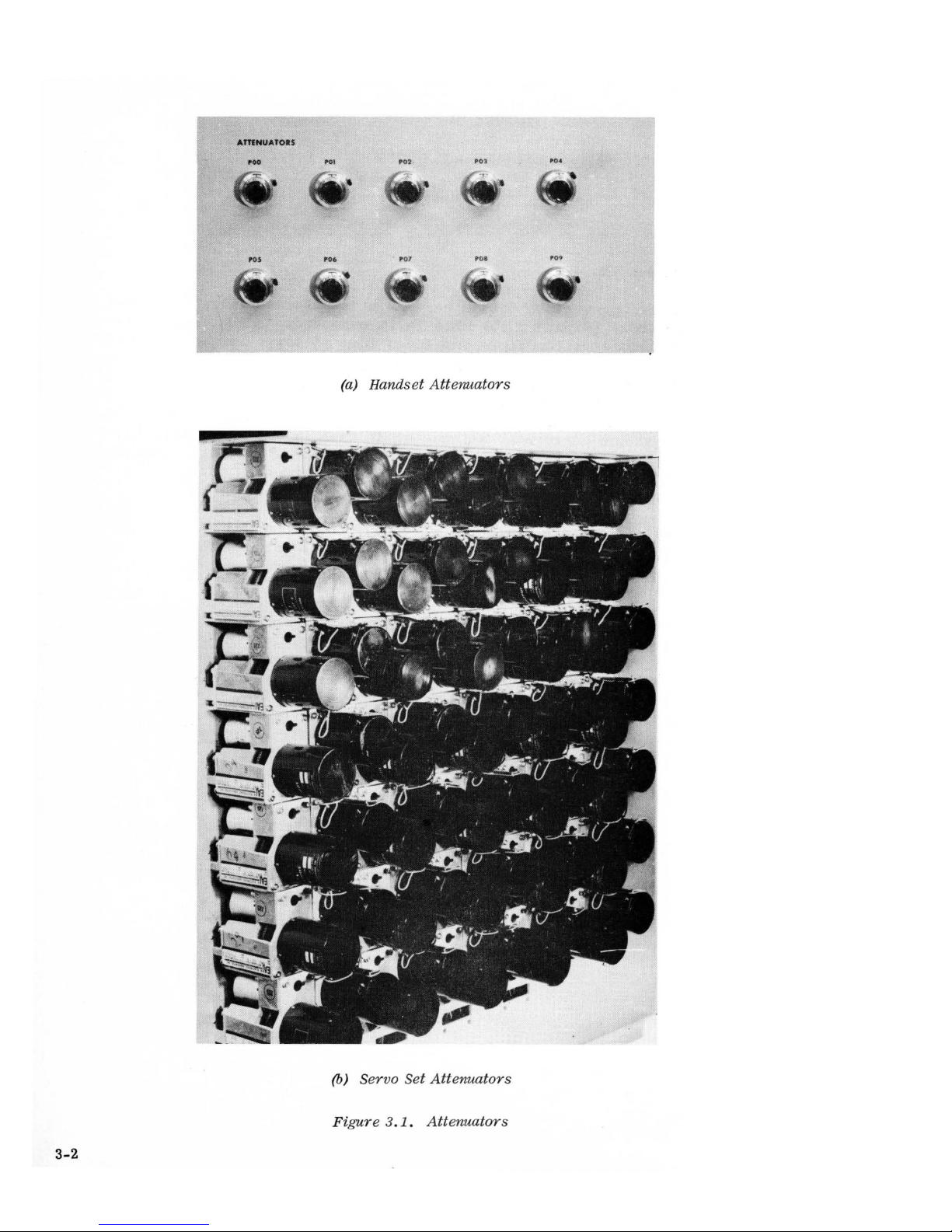
3-2
AmNUA
TOIS
'00
...
,
....
,.
,
POl
'0.
'06
'
07
••
1
,.9
(a) Handset Attenuators
(b) Servo Set Attenuators
Figure
3. 1 . Attenuators
Page 50

r-CI---_
~+REF~
__
---4
x
COEFFICIENT
~E:TING
X
--k!)---
KX
HI
Lo
---t'lo-·.
SIMPLIFIED
DIAGRAM
TO
SELECTOR
CIRCUIT
SCHEMATIC
(a)
Grounded Potentiometer
x
Y
HI
Lo
KX
K(Y-X)+Y
~TENTIOMETER
NUMBER
COMPUTER DIAGRAM
SYMBOL
X
K
(X-Y)+Y
Y
--Qoo-
SIMPLIFIED
..
~
TO
CIRCUIT
DIAGRAM
SELECTOR
SCHEMATIC
(b) Ungrounded Potentiometer
3.2.
Figure
Potentiometer Configurations
COMPUTER DIAGRAM
SYMBOL
3-3
Page 51
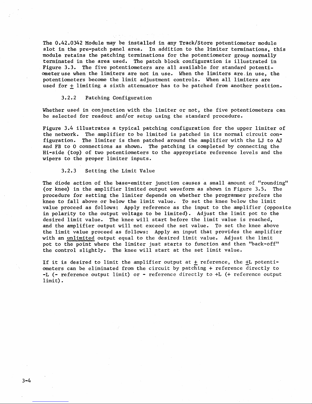
The
0.42.0342
slot
in
the
module
terminated
Figure
ometeruse
potentiometers
used
retains
3.3.
when
for ± limiting
Module
pre-patch
the
in
the
The
five
the
become
may
be
panel
patching
area
used.
potentiometers
limiters
the
a
sixth
installed
area.
terminations
The
are
not
limit
adjustment
attenuator
In
patch
are
in
in
any
addition
for
block
all
use.
controls.
has
to
Track/Store
to
the
the
potentiometer
configuration
available
When
be
the
patched
potentiometer
l~miter
for
limiters
When
from
terminations,
group
is
illustrated
standard
are.in
all
limiters
another
module
normally
potenti-
use,
are
position.
this
in
the
3.2.2
Whether
be
selected
Figure
the
figuration.
and
Hi-side
wipers
3.4
network.
FB
to 0 connections
to
3.2.3
The
diode
(or
knee)
procedur'e
knee
with
to
value
in
polarity
desired
and
the
the
limit
an
pot
to
the
control
proceed
the
Patching
used
in
for
illustrates
The
The
(top)
fall
limit
amplifier
unlimited
the
action
in
the
for
above
to
value
point
slightly.
of
proper
Setting
setting
as
value.
conjunction
readout
amplifier
limiter
two
potentiometers
limiter
the
of
the
amplifier
the
or
below
follows:
the
output
The
output
proceed
output
where
Configuration
with
and/or
a
typical
to
is
then
as
shown. The
Limit
base-emitter
limited
limiter
the
Apply
voltage
knee
will
as
follows:
equal
the
limiter
The
knee
the
setup
patching
be
patched
inputs.
Value
limit
reference
will
not
to
will
limiter
using
limited
patching
to
the
junction
output
depends
value.
to
be
start
exceed
Apply
the
desired
just
start
or
not,
the
standard
configuration
is
patched
around
waveform
on
as
limited).
before
the
an
starts
at
the
is
appropriate
causes a small
whether
To
the
set
input
limit
to
the
the
in
amplifier
completed
as
shown
the
set
the
input
Adjust
the
limit
value.
that
value.
function
set
limit
five
procedure.
for
the
its
normal
with
by
reference
amount
in
programmer
knee
below
to
the
the
value
To
set
provides
Adjust
and
value.
potentiometers
upper
connecting
levels
Figure
amplifier
limit
is
the
then
limiter
circuit
the
LJ
of
"rounding"
3.5.
prefers
the
pot
reached,
knee
the
amplifier
the
limit
"back-off"
and
limit
(opposite
to
above
con-
to
the
the
can
of
AJ
the
The
the
If
it
is
ometers
-L
(-
limit)
desired
can
be
reference
•
to
limit
eliminated
output
3-4
the
from
limit)
amplifier
the
or -reference
output
circuit
at ± reference,
by
patching
directly
+
reference
to
+L
the
(+
reference
±L
potenti-
directly
to
output
Page 52

+
HI
O
LJ
e
F8 e
LJ
e
-L
0
+l
()
- L 0
+l"
POT-LIMITER
0.420342
Fi
gure
3.
3.
F
eed
back
Limiter
Patching Block
(a) Computer
Diagram
FBO
LJO
+LO
(b)
Patching
Diagram
FBO
-LO
POT-LIMITER
0.42.
0342
Fi
gure
3.
4.
Typical
Limiter
Patching
3-5
Page 53
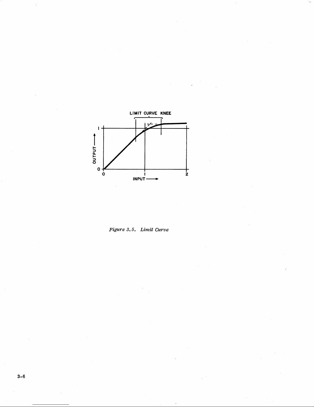
1
~
~
a..
~
:::)
0
LIMIT
CURVE
.
KNEE
Figure
INPUT~
3.
5.
I
Limit
2
Curve
3-6
Page 54
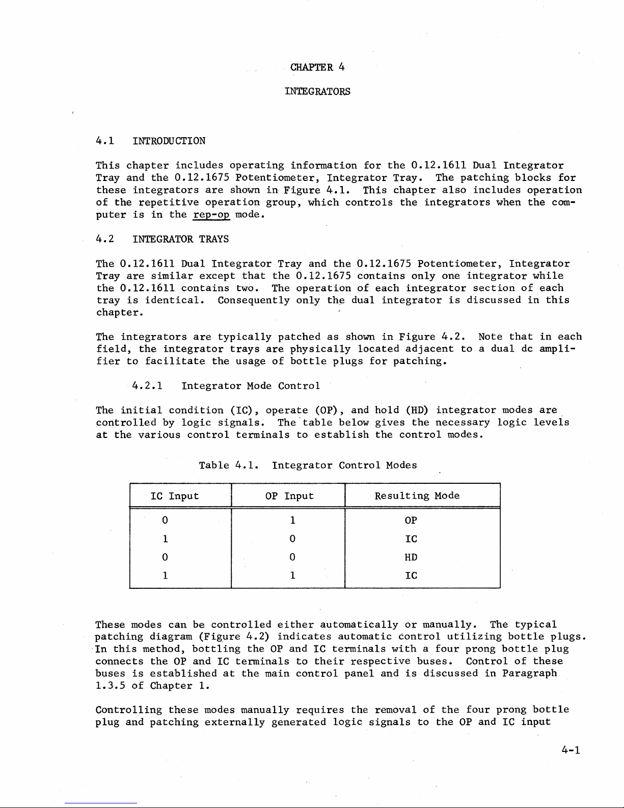
INTEGRATORS
4.1
This
Tray
these
of
puter
4.2
The
Tray
the
tray
INTRODUCTION
chapter
and
integrators
the
repetitive
is
INTEGRATOR
0.12.1611
are
0.12.1611
is
chapter.
The
integrators
field,
fier
the
to
4.2.1
The
initial
controlled
at
the
various
includes
the
0.12.1675
in
the
Dual
similar
contains
identical.
integrator
facilitate
Integrator
condition
by
logic
are
operation
rep-op
TRAYS
Integrator
except
are
the
control
operating
Potentiometer,
shown
in
group,
mode.
Tray
,that
two.
the
The
Consequently
typically
trays
usage
Mode
(IC),
signals.
patched
are
of
Control
operate
The
terminals
information
Integrator
Figure
4.1.
which
and
0.12.1675
operation
only
th~
as
physically
bottle
(OP),
'table
to
establish
controls
the
dual
shown
plugs
and
below
for
the
Tray.
This
chapter
the
0.12.1675
contains
of
each
integrator
in
Figure
located
for
patching.
hold
gives
the
control
0.12.1611
The
also
integrators
Potentiometer,
only
one
integrator
is
4.2.
adjacent
(HD)
integrator
the
necessary
modes.
Dual
Integrator
patching
includes
when
integrator
section
discussed
Note
to a dual
modes
logic
blocks
operation
the
com-
Integrator
while
of
each
in
this
that
in
dc
ampli-
are,
levels
for
each
These
modes
patching
,In
this
connects
buses
1.3.5
is
of
Controlling
plug
and
IC
Table
Input
4.1.
Integrator
Input
OP
Control
0 1
1
0
0 IC
0
1 1 IC
can
be
diagram
method,
the
OP
established
Chapter
these
patching
controlled
(Figure
bottling
and
IC
at
1.
modes
externally
4.2)
terminals
the
manually
the
main
either
indicates
OP
and
to
control
requires
generated
automatically
automatic
IC
terminals
their
respective
panel
the
logic
signals
Modes
Resulting
OP
HD
or
control
with a four
buses.
and
is
removal
to
Mode
manually.
utilizing
prong
Control
discussed
of
the
the
OP
four
and
The
bottle
bottle
in
Paragraph
prong
IC
typical
of
these
bottle
input
plugs.
plug
4-1
Page 55

4-2
(a)
Dual
Integrator
OJO
IJO
cO
leO
OFASTO
o
pO
Ole
0
POT-I
NTEGRATOR
0.12.1675
(b)
Single
Integrator
(With
Attenuator
Terminations)
Figure
4
.1.
Integrator
Patching
Blocks
Page 56
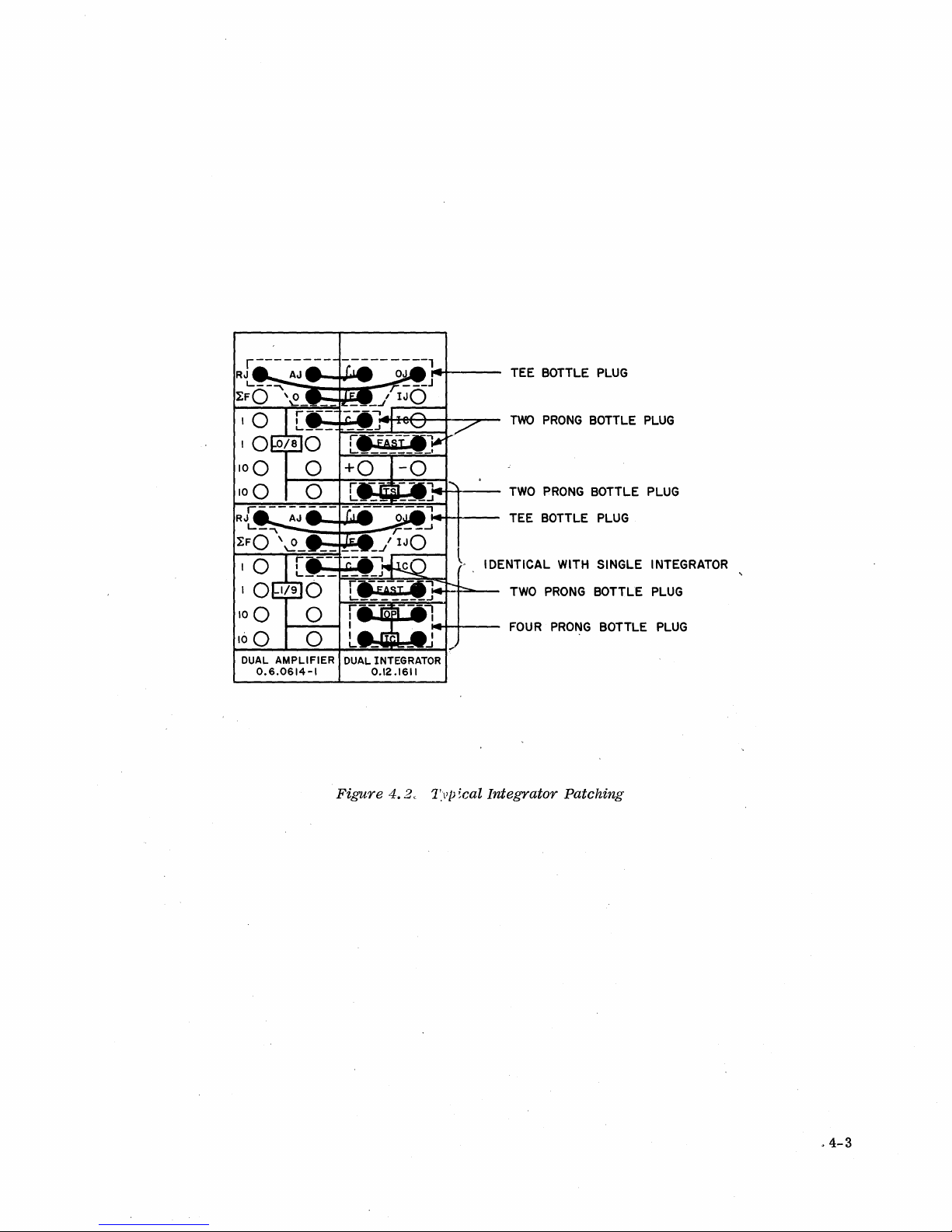
TEE BOTTLE
TWO
PRONG
PLUG
BOTTLE
PLUG
~~~~~~~~~~~::~
DUAL
AMPLIFIER
0.6.0614-1
W'-Wliit-......
DUAL
INTEGRATOR
0.12.1611
Figure
4.2,
l'yp
-+---
TWO
PRONG
TEE BOTTLE
BOTTLE
PLUG
IDENTICAL WITH SINGLE INTEGRATOR
TWO
~cal
Integrator
PRONG
FOUR
PRONG
Patching
BOTTLE
BOTTLE
PLUG
PLUG
PLUG
,4-3
Page 57
(green)
desired
patch
mode.
terminals.
Refer
to
Table
4.1
for
the
proper
logic
signals
for
the
4.2.2
Each
0.002
and
integrator
~f)
0.2
resistor.
scale)
and
Bottling
bus'.
The
buttons
is
described
provides
levels
can
relay.
it
in
the 2 ms
terminal
The
FAST
increasing
by
paralleling
paralleling
Table
time
4.2
constants.
Integrator
is
which
provide
millisecond
Capacitor
the
proper
the
TS
patch
logic
on
the
access
be
A low
levels
main
in
Paragraph
to
patched
(grd)
state
de-energizes
terminals,
the
value
the
the
0.002
gives
the
Capacitor
provided
with
time
respectively
selection
patching
terminals
in
this
control
panel.
1.3.5
the
TS
input
to
this
patched
to
while a high
the
TS
when
1
of
the
~f
capacitor
~f
bottled,
integrator
capacitor
necessary
Selection
four
constants
when
is
determined
of
the
connects
bus
are:
of
Chapter
(green)
terminal
the
TS
(+
relay
patching
placing
effectively
with
with a 0.018
capacitors
of 1 second,
used
with a standard
FAST
input
the
controlled
The
operation
1.
terminal.
to
provide
terminal
voltage
it
feedback
a 9
~f
and
time
(10
by
logic
terminals.
TS
input
of
Removal
manual
energizes
or
no
in
the
slow
capacity.
capacitor
~f
scale
~f, 1 ~f,
001
second, 2 milliseconds,
gain-of-one
levels
to a master
by
the
TIME
the
TIME
of
the
Externally
control
the
connection)
IS
state.
down
computer
This
in
the
capacitor
selection
0.02
on
the
time
SCALE
SCALE
TS
bottle
generated
of
TS
relay
patched
operation
is
accomplished
IS mode
in
the 2 ns
for
~f,
and
(lOOK)
TS
(time
scale
push-
pushbutton
plug
logic
the
TS
placing
to
the
by
and
mode.
different
Any
integrator
used
as
below
the
bottle
prong
put.
maining
4.3.
TIME
SCALE
Switch
SEC
1
1
SEC
2
MS
2
MS
4.2.3
1)
an
describes
plug
bottle
Patch
the
gain-of-one
If
the
Additional
not
used
extra
these
4.2.3.1
between
plug
between
signals
four
prong
Table
4.2.
FAST
Terminals
Bottled
Not
Bottled
Bottled
Not
Bottled
Integrator
for a particular
D/A
switch,
additional
D/A
Switch.
the C terminal
an
amplifier
to
be
amplifier
bottle
Time
Uses
and
uses
To
switched
inputs.
plug
is
Constant
Selection
Feedback
Capacitor
10
~f
1
Ilf
0.02
0.002
problem
2)
as a differentiator.
for
the
use
and
~f
integrator.
the
integrator
the
amplifier
~f
can,
gain-of-one
in
the
IC
patch
The
resulting
left
in
the
by
input
circuit
OP
and
Time
(with
1.0
0.1
2.0
0.2
proper
as a D/A
output.
and
terminal
IC
Constant
lOOK
SEC
SEC
MS
MS
patching,
The
the
amplifier
and
is
shown
patch
Input)
be
paragraphs
switch,
Connect
the
on
a two
re-
Figure
terminals,
remove
out-
4-4
Page 58

1:
F
--.J\/\JIv----
10
---'\!\f1v----_
10
----".J\!\,----
o
........
......
Figure
4.3.
Integrator Used as a
D/
A Switch
4-5
Page 59

the
D/A
switches
independently
patching
external
of
operate
the
REP-OP
logic
at
the
rate
signals
REP-OP
by
removing
to
the
rate.
OP
and
The
the
IC
D/A
four
input
switches
p~ong
bottle
(green)
can
patch
be
operated
plug
and
terminals.
entiator
bottle
Select
the
signal
entiated
4.2.3.2
remove
plug
the
signal
the
bottle
between a gain-of-one
desired
to
capacitor
be
differentiated
appears
Differentiator.
plug
from
value
to
at
the
output
To
the C patch
amplifier
(see
Paragraph
the C patch
of
the
operate
input
terminal.
amplifier.
the
integrator
terminal.
and
the
4.2.2,
Connect
amplifier
this
chapter).
The
resultant
as a differ-
two
prong
output.
Patch
differ-
4-6
Page 60

CHAPTER
5
5.1
This
pliers
include
Square
Each
duce a four
plication,
multipliers
terminals
This
additionally,
5.2
Since
Quarter-Square
Figure
is
'patched
in
INTRODUCTION
chapter
used
the
Multiplier,
of
these
to
provision
MODEL
the
patch
5.2
patched
to
Table
5.1.
provides
in
the
0.7.0146
multipliers
quadrant
each
of
in
the
permit
allows
for
0.7.0146
blocks
Multipliers
is a simplified
to
an
amplifier
simplify
information
580
Computer.
High
and
the
product
the
multipliers
0.7.0146
patching
the
squaring
AND
and
the
QUARTER-SQUARE
on
the
The
multipliers
Accuracy
0.7.0150
are
of
and
each
upper
and
0.7.0148
patching
are
diagram
in a typical
diagram.
Quarter-Square
Quarter-Square
used
in
conjunction
two
variables,
is
also
0.7.0148
squaring
multipliers
square
identical,
root
QUARTER-SQUARE
procedures
of
the
The
function
MULTIPLIERS
operation
X
and
capable
Trays
configuration.
are
circuit
in
these
fUnctions.
MULTIPLIERS
for
only
the
multiplier.
of
of
the
available
Multiplier,
Multiplier
with
each
dc
Y.
In
of
division.
provided
separately
trays
the
0.7.0146
0.7.0146
Note
The
input
quarter-square
in
the
580
the
0.7.0148
(Figure
amplifiers
addition
The
with
to
extra
(Figure
be
utilized,
and
is
described
that
inputs
terminal
0.7.0148
the
are
multi-
Computer
Quarter-
5.1).
to
pro-
to
multi-
upper
patching
5.2a).
below.
multiplier
not
shown
is
given
Patch
Figures
squaring,
(upper
functions
The
output
external
vided
for
5.3
and
and
lower)
(Figures
amplifiers
feedback
this
Terminal
lA
lB
lC
lD
2C
2B
2A
2D
through
square
has
resistor
purpose
Table
5.6
root
5.5
5.1.
show
functions
only
one
and
5.6)
patched
patched.
in
the
Multiplier
Function
+X
+y
-X
-Y
+X
+Y
-X
-Y
multiplier
respectively.
feedback
the
upper
to
YJ
in
0.7.0148
patching
resistor.
squaring
the
A
feedback
Multiplier.
Input
0.7.0146
Functions
squaring
+
multiplier
squaring
-
multiplier
+
squaring
multiplier
squaring
-
multiplier
for
resistor
Destination
card
card
card
card
multiplication,
Note
For
that
squaring
cards
Multiplier
are
(3.55K
in
upper
upper
in
lower
in
lower
in
each
multiplier
and
patched
must
ohms)
division,
square
separately.
have
is
an
pro-
roots
5-1
Page 61

·
-,
r
r
MULTIPLIER
0.7.0148
(a)
O.
7.0146
Dual
Multiplier
(b)
0.7.0148
Multiplier
(c)
0.07.0150
Multiplier
Figure
5.1.
Quarter-Square
Multiplier
Patch
Blocks
5-2
Page 62

PLUS
SQUARING
MINUS
SQUARING
PLUS
SQUARING
MINUS
SQUARING
(a)
Upper Multiplier
PLUS
SQUARING
Figure
MINUS
SQUARING
PLUS
SQUARING
MINUS
SQUARING
(b)
Lower
5.2.
Multiplier
Quarter-Square Multiplier,
Simplified
Diagram
5-3
Page 63

OUTPUT
UPPER MULTIPLIER
FROM
OUTPUT
LOWER MULTI
FROM
Figure
PLI
ER
5.3.
Multiplier Patching
+X
-'---
- X
-;:::=!~~~==t'-
~---
------,
.........
~~~==~~---
DUAL MULTIPLIER
0.7.0146
for
Multiplication
_.......&...-
+y
-y
+X
-y
--y
+y
5-4
Page 64

E
o -X-
X
---'---1
- A
Figure
+yO
DUAL MULTIPLIER
5.4.
Multiplier Patching
-yO
0.7.0146
for
Division
5-5
Page 65
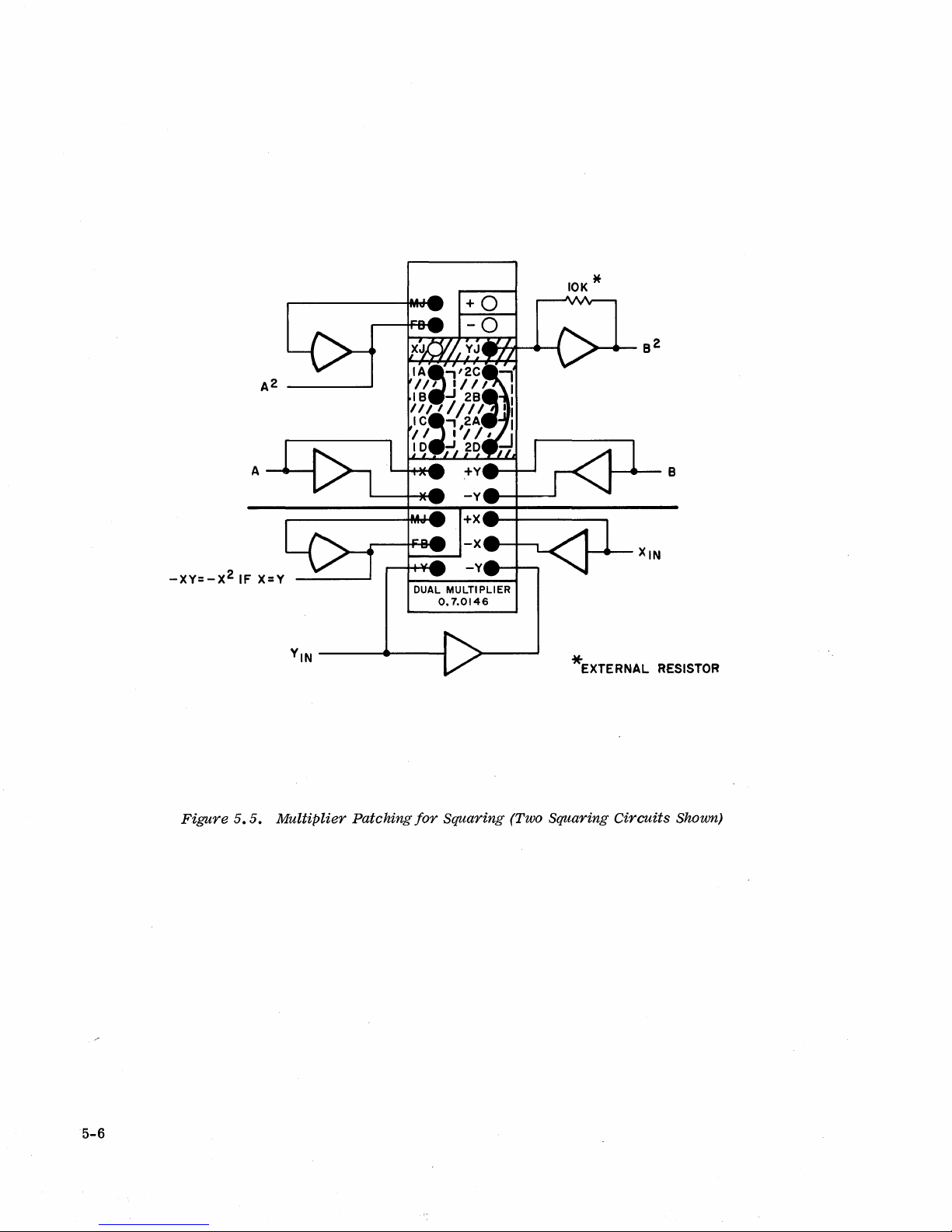
10K
*
1--
.....
- B
-XY=-X
Figure
2
5.5.
IF
X=Y
YIN
---
Multiplier
......
----1
Patching
DUAL
MULTIPLIER
0.7.0146
for
Squaring (Two Squaring
*EXTERNAL
Circuits
RESISTOR
Shown)
5-6
Page 66

+~
-+----<
FBO
+yO
DUAL
MULTIPLIER
0.7.0146
_-Jv'Vv---
-"""""---ITeT
*EXTERNAL
B
OSBS+IOV
RESISTOR
Figure
5.6.
Multiplier Patching
for
Square
Root
5-7
Page 67

5.3
The
0.7.0150
circuits,
by
any
Chapter
MODEL
patching
particular
8.
0.7.0150
QUARTER-SQUARE
Quarter-Square
for
two
problem.
Multiplier
MDFG
The
units
MDFG
MULTIPLIER
(Figure
and
two
readout
patch
5.1c)
free
includes
diodes
terminals
for
two
use
are
multiplier
as
required
described
in
Operationally,
multipliers
feedback
patch
resistor
holes
multiplication
Figures
5.7
each
in
have
and
and
the
been
5.8.
of
the
0.7.0146
patch
relocated.
division
multipliers
and
terminal
functions.
0.7.0148
is
identified
These
in
this
Trays
multipliers
Patching
tray
are
(Figure
as
FJ
are
for
identical
5.2b).
instead
capable
these
to
Physically,
of
FB,
of
functions
the
lower
the
and
the
performing
is
shown
in
5-8
Page 68
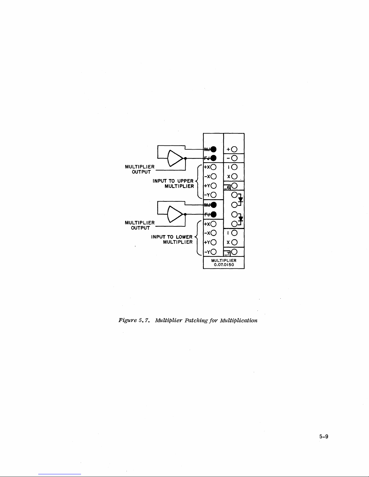
MULTIPLIER
OUTPUT
INPUT
MULTIPLIER
TO
UPPER
{+XO
-xO
+yO
-yO
+0
-0
10
xO.
o
g}
MULTIPLIER {
OUTPUT
INPUT
TO
LOWER
MULTIPLIER
Figure
5.7.
Multiplier Patching
+xO
-xO
+yO
-yO
~~",&::,::..J....;;.~
MULTIPLIER
for
00·
j"
I 0
X 0
_70
0.07.0150
Multiplication
5-9
Page 69
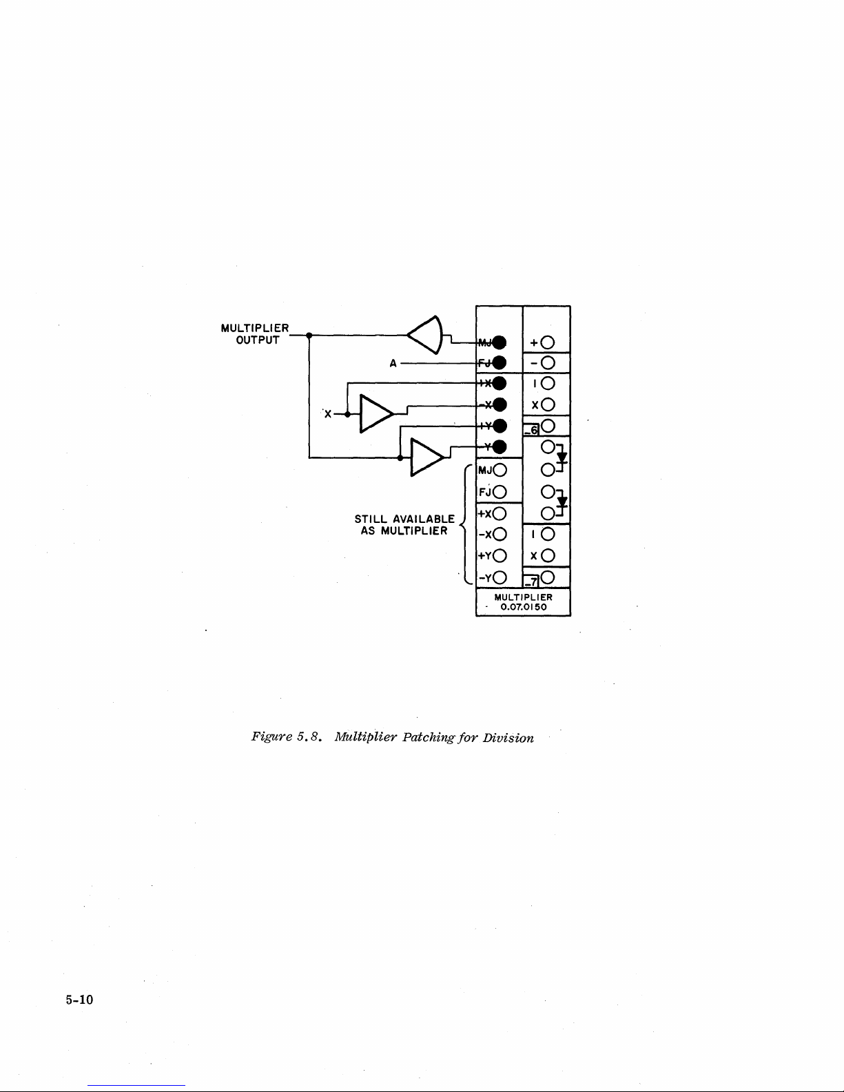
MULTIPLI
OUTPUT
ER_
.......
____
STILL
AS
MULTIPLIER
--<
A
---~IoFd-I_
AVAILABLE
'--....;;;..---I--~-4
MULTIPLIER
-
0.07.0150
+0
-0
10
xO
o
Figure
5-10
5.8.
Multiplier
Patchingfor
Division
Page 70

'CHAPTER
'6
6.1
INTROPUCTION
The Log X DFG's
an
output
.
Common
The
inputs
paragraphs
basic
magnitude.
and
unit
voltage
natural
and'outputs
arel
of
A
unit-scaling
6.2
The Log X
OPERATING
DFG,
generators.
an
output
ative
input
voltage
voltage
operate
that
is
logarithms
for
given
on
measurement
description
and
voltage-scaling
CONSIDERATIONS
Model
Two
0.,~6.0355,
of
the
of
-1/2
X
and
The
abbreviation
to
the
for
natural
LOG X DIODE
in
conjunction
proportional
and
antilogarithms
the
circuit
a
u~it-scaled
so
that
all
of
unit-scaling
is
consists
generators
10glO
proauce
accept a positive
(-IOOX).
an
log
base
10.
The
logarithms
FUNCTION
with
to
the
conf{gurations
basis.
properly
and a tabulation
given
in
of
The
output
voltage
NOTE
indicates
abbreviation
(to
GENERATORS
an
operational
logarithm
can
Computer
scaled
Appendix
four
independent
other
the
the
base
of
be
generated.
described
reference
voltages
4.
input
two
generators
of
1/2
logarithm
In
is
used
e).'
amplifier
the
input
are
of
outputs
in
is
to
voltage
the
following
taken
~1.0
for
logarithmic
voltage
X
and
accept a neg-
10glO C:"lOOX).
produce
•
as
unit
in
both
function
produce
A
simplified
are
.independent
patching
occupied
resistor
described
6.3
The
voltage
a
omet~rs.
OPERATING
patching
is
variable
Although
the
associated
schematic
and
terminations
by two
used
in
MDFG
as
free
Chapter
INSTRUCTIONS
for
the
restricted
input
Care
doing
impedance,
should
so
wiil
amplifiers
of
the
each
has a resistor
occupy
amplifier
components.
8.
DFG's
is
to a range'of
input
be
taken
not
harm
in
10g.X
the
left
patch
The
illust'rated
voltages
not
to
the
certain
DFG
is
shown
associated
side
of
terminations
MDFG
in
0.01
to
should
apply
DFG,
it
circuits.
in
the
patch
and
amplifier
Figure
1.0
(reference).
never
an
input
can
constitute
Figure
with
two
patch
6.2.
voltage
6.1.
it.
The
block.
diodes
terminations
Note
be
obtained
of
a
severe
The
log X DFG
The
and
that
Since
the
four
right
a 100
are
the
input
the
DFG
from
potenti-
wrong
overload
DFG'~
side
is
ohm
has
polarity.
on
6-1
Page 71
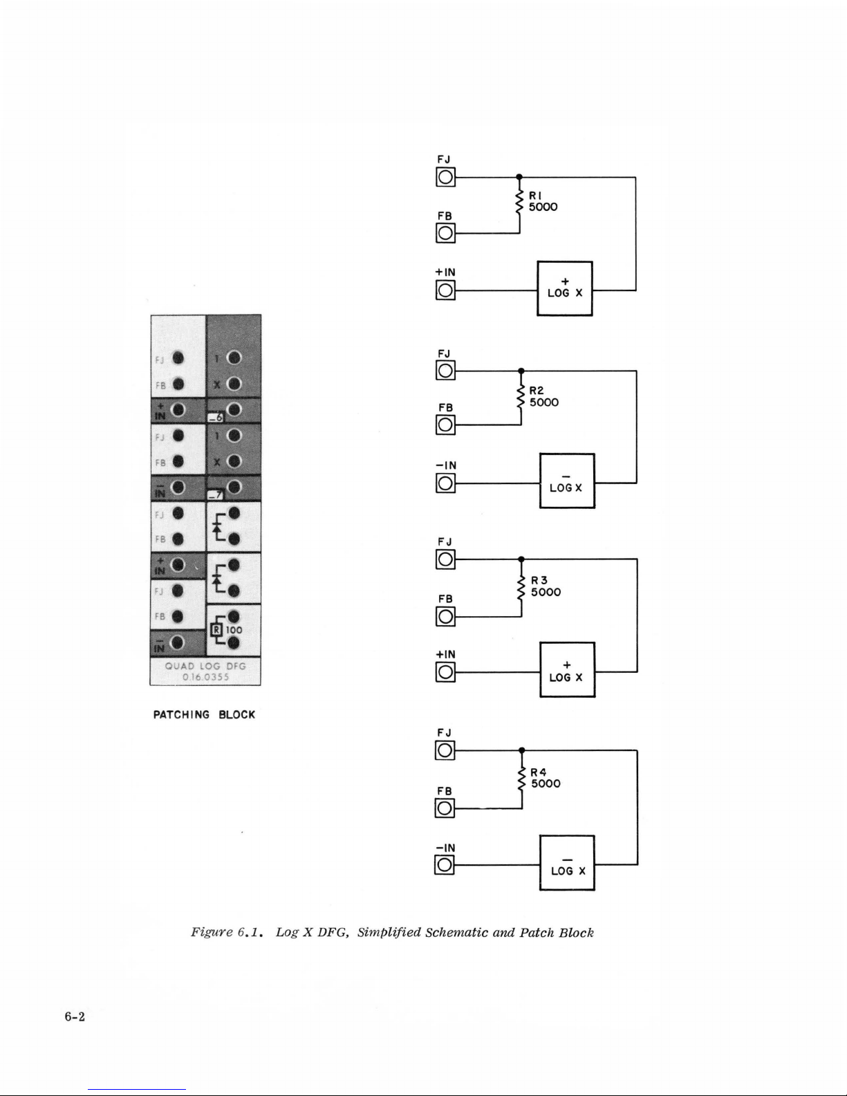
RI
5000
FB
0
+IN
0
+
LOG
X
FJ
0
R2
FB
5000
0
-IN
0
LOGX
FJ
0
R3
FB
5000
0
+IN
0
+
LOG
X
PATCHING
BLOCK
FJ
0
R4
FB
5000
0
-IN
0
LOG
X
Figure
6.1.
Lo
g X DFG,
Simplified
Schematic
and
Pat
ch
Block
6- 2
Page 72

-1/2
LOG
(+100 X )
+XIN
( X
+
-XIN
(XIN
IN
1/2
POSITIVE)
LOG
(-IOOX)
NEGATIVE)
FBO
INa
FJO
QUAD
~o
LOG
DFG
0.160355
Figure
6.2.
+X
+IN
+X
-IN
NOTE:
1.
Log X DFG
+LOG
-LOG
(.01)
REFERENCE~lxINI
VOLTAGE.
Patching
:5REFERENCE
-
+
(-100
1/2
1/2
LOG
(lOOX)
LOG
X)
6-3
Page 73
THE
TRACK-STORE,
CHAPTER
D/A
7·
SWITCH
TRAY
7.1
The
patching
patching
two
Chapter 3 of
circuits
7.2
The
electronic
control
Figure
fier
TF
is
terminal
the
terminal
capacitors.
When
the
the T terminal
Consequently,
store
INTRODUCTION
Model
D/A
0.42.0341
terminations for
for
switches.
(TIS
THE
TRACK-STORE
track-store
circuitry.
7.3
is
patched
are
patched
patched
(track
unit
TJ
in
provides
the
track
terminal
mode when
five
attenuators
A
this
manual,
and
D/A)
(TIS)
switches
gives
to a logic
typical
to
to
IC
the
IC
(T)
with
causes
the
the T input
terminal
amplifier
input
mode.
an
input
unit
Potentiometer,
three
(-5
description
and
is
are
described
CIRCUIT
circuit
(track,
TIs
signal
on
input
is
SWJ,
the
is
(Figure
long
patching.
TJ.
terminals
which
Figure
It
overrides
for
high,
and
the
track
in
the
goes
Track-Store,
different
through
of
the
not
store,
The
controls
7.2)
the
analog
the
store
switch
track
low.
D/A
types
-9),
attenuator
discussed
in
the
7.2)
and
The
switch
AJ
and 0 respectively.
is
the T logic
initial
track
electronic
to
open
mode when
of
one
in
following
consists
short
resistor
junction
the
mode
patched
electronic
and
Tray
circuits.
track-store
operation
this
of
store),
to a logic
control
condition
switches
the
the T input
(Figure
chapter.
paragraphs.
storage
an
junction
(SWJ)
of
the
switch
store
7.1)
These
(TIS)
is
included
The
capacitors,
IC'network,
(RJ)
terminal
Terminal
unit.
signal
signal.
voltage
is
closed
are
open.
switch
is
high
has
include
unit
remaining
of
an
and
T
The
lower
which
The
upper
for
connecting
A low
to
close.
and
and
in
three
and
a
ampli-
terminal
(track)
IC
places
IC
the
store
at
in
the
A
high
minal
rivative
capacitors
7.3
The
patching
A
age
holds
The 10
switched
D/A
logic
level.
at
the
to
the
readout.
THE
D/A
switch
terminals
signal
the
switch
terminal
is
(track)
D/lO
to
the
SWITCH
and
at
A
high
patched
selector
A
IC
its
(Figure
this
(+Sv)
in a non-conducting
is
lOX
IC
second
analog
control
point
(10K)
at
this
terminal
switch
set
voltage
704).
turns
causes
times
terminal.
energizes
on
of
input
The
the
the
relay
through
are
SW
the
switch
switch
state.
input
a
relay
main
contro'l
contacts
the
IC
terminated
terminal
on
to
conduct
of
the
switchw
which
panel,
permits
terminal.
at
provides
or
off
while
connects
permitting
charging
the
SW,
a
control
depending
a low
Any
analog
10,
the
the
and
on
(0
TJ
store
SWJ
input.
its
volt)
input
a
volt-
terde-
to
be
7-1
Page 74

Figure
7.1.
Track/store,
D/ A Switch
Patch
Block
7-2
Page 75

T
TJ
OJ-----+--4I~o-~
0110
~--4-----I----~
lOOK
Ie
OJ-----4--------~~~--------~--~------~~----------~
10K
--------------1
10K
I
I
I
I
I
I
I
I
I
I
KI
-20V
Figure
7.2.
Track/store
Circuit,
Simplified
Diagram
7-3
Page 76

--'oIV",----
~~~R~J~--~~--
IF
10
10
TRACK CONTROL
INPUT
L~~-.L-~==t--
_--11'--_
____________
Figure
7.3.
T/S
Patching
----
'-_+-_
__
(Typical)
ANALOG
CONDITION
TRACK
INITIAL
IC
INPUT
7-4
Page 77

LOGIC
---t::::=::===:;===:::=9
SIGNAL
ANALoGi-----:==~~=R~-IO-;81~::i
INPUT
SWO
Figure
o
7.4.
D/ A Switch
POT-T/S-
0.42.0341
Patching
SWJ
O/A
(Typical)
7-5
Page 78

The
the
is
SWJ
(switch
device
patched
(the
to
junction)
amplifier
this
terminal.
terminal
in
Figure
is
7.3)
the
output
recovering
of
the
the
switch.
switched
The
input
analog
of
voltage
7-6
Page 79

8
1
INTRODUCTION
0
The
MDFG
by means
ment
A
8.2
in
fully
pairs,
operations
LOCATION
segment
the
analog
allows
of
expanded
and
the
generation
straight-line
are
possible.
AND
ADDRESSING
580
contains
each
pair
may
DFG's. The DFG's
patch
panel.
CHAPTER
THE
of
segment
8
be
used
are
located
8
MDFG
arbitrary
continuous
approximation.
ten-segment
DFG's. The DFG's
as a twenty-segment
in
slideout
non-linear
Both
ten
drawers
and
DFG
directly
or
twenty
are
as
functions
seg-
arranged
two
ten-
below
Each
patching
pair
of
area.
DFG's
the F pushbutton
address
77.
dresses
pair
plifier
for
each
In a ten-segment
given
(the
one
of
the
In a standard
capable
of
accepting
tive
on a
tray
8.3
The
sion
applications
and
804
Since
of
straight-line
termine
curve
cal
table
in
tabular
is
usually
sent
of
accepting
negative
or
negative
separate
(8
.lb).
APPLICATIONS
main
application
of
an
additional
such
combined summation
SETUP
as
form,
of
the
diode
the
smoothly
and
values
PROCEDURE
location
form - a
the
the
result
are
To
address a DFG
and
the
of
the
above.
ending
in
second
computer
positive
outputs.
tray
(8.la)
for a DFG
as
the
function
segments,
of
as
possible.
the
programmer
of x and
table
result
of a series
terminated
numerical
MDFG
operation
for
pairs
each
on a single
readout,
address
is
F46,
MDFG
In a twenty-segment
-6)
uses
all
twenty
DFG
(the
one
ending
configuration,
inputs.
inputs.
Either
Figure
and
the
is
input
and
resistor
use
of
function
generator
the
first
the
breakpoints
the
the
The
type
8.1
shows
patching
function
for
unused
generation.
approximates a given
step
Usually
must
f{x)
of
values
of
experimental
of
determine,
for
setup.
of x and
measurements,
calculations.
patch
it
on
the
47,
F56,
is
addressed
operation
segments
in
-7)
first
DFG
second
of
DFG
the
MDFG
terminations
generation;
each
DFG
output
in
the
("corners")
the
desired
by
inspection
Sometimes
f(x).
block
is
necessary
main
control
57,
using
the
leaving
available
in a pair
DFG
is
can
produce
patching
however,
allows
amplifier
setup
in
of
order
curve
the
Such a
although
in
the
to
F66,
67,
one
first
DFG
the
as
an
is
a -DFG,
either
terminations
on a
mUlti-purpose
some
alternate
as
curve
any
by'a
DFG
to
is
given
of
the
function
table
it
analog
depress
panel.
and
of
in
output
inverter.
the
capable
the
an
inverter,
is
fit
in
graph,
is
o'f
may
The
F76,
the
each
+DFG,
posi-
inclu-
series
to
the
graphi-
given
values
repre-
ad-
am-
de-
a
8-1
Page 80
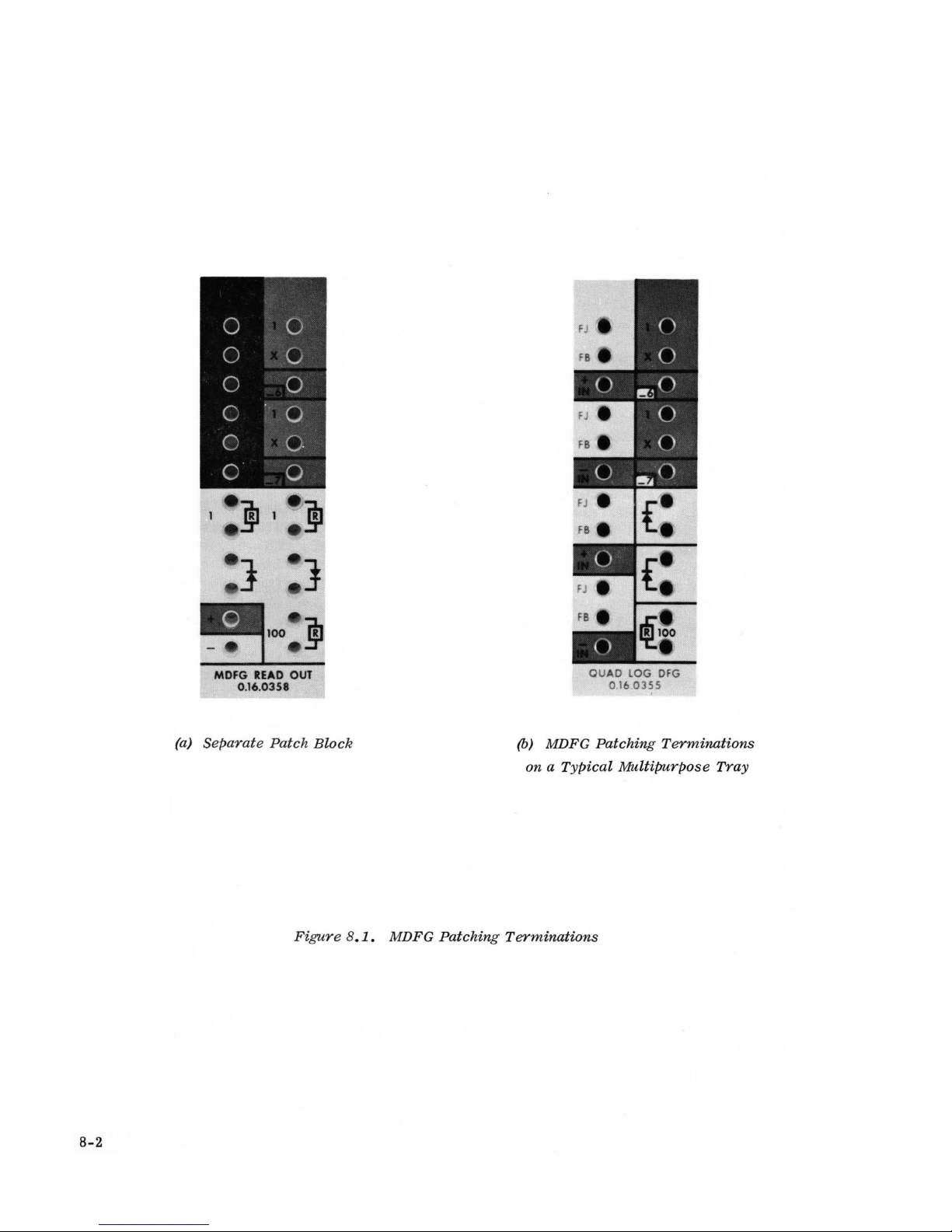
8-2
0
0
0
0
0
0
c
0
c
0·
c
0
[J
-]I
1 R
-
eJ
]
'!'
~wo
.~
,
MDFG
READ
OUT
0.16.0358
(a)
Separate Patch
Block
QUAD
lOG
DFG
0160355
(b)
MDFG
Patching
Terminations
on a
Typical
Multifmrpose
Tray
Figure
8.1.
MDFG
Patching
Terminations
Page 81

If
the
function
the
DFG
to
ber
of
data
ments
available
distribution
be
the
best
For
example,
values
to
to
a good
sirable
which
of
use
equally-spaced
plot
the
breakpoint
to
means
is
the
values
points
in
of
the
distribution
the
original
the
input
data
points,
know
it
"what
should
given
of x and
in
the
the
DFG.
data
variable
breakpoints
location
the
be
in
tabular
table
The
points
of
breakpoints
data
may
x,
pass
a smooth
from
function
plotted
form
f(x)
from
happens
difficulty
that
have
whereas
for
this
looks
before
it
the
to
define
for
been
it
segment
curve
smooth
like"
setup.
is
tempting
table,
coincide
with
the
especially
with
this
function
straight-line
obtained
is
generally
approximation.
through
graph.
In
before
to
simply
the
approach
~ll
approximation.
for
equally-spaced
~
them,
any
and
case,
trying
if
number
is
probably
a
good
It
determine
to
set
set
the
that
is
it
of
idea
better
is
it
up
num-
segthe
not
de-
up,
Hence,
tion
setup
is
defined
breakpoint
and
setting
a
setup
the
An
alternate
panel
input x and
consists
exactly
Even
the
make
if
DVM,
sure
the
the
be a part
listing
cludes
venient
pletely
of
an'
plotting
set
8.4.1
Although
tion,
they
With a bit
timum
ing
breakpoint
general
procedure
graphically.
locations,
up
the
that
output
procedure,
of
setting
same,
function
it
is
a good
that
the
of
the
pot-settings,
integrator
up
and
Breakpoint
there
exist
generally
of
experience,
rules
tabulating
function
permits
up
but
the
is
idea
function
problem
capable
without
the
analytical
require
location
may
serve
in
this
chapter
The
procedure
the
from
this
the
direct
f(x)
may
be
read
illustrated
the
function
operator
set
up from a
to
has
looks
obtain a continuous
been
documentation,
assignment
of
generating
patching
resulting
changes.
curve
Location
methods
too
much
a good programmer
Simply by
as a rough
assumes
values
table
setup
directly
in
Paragraph
of
an
X~y
at
the
table
set
up
along
sheets,
a ramp
plotted
for
computation
can
inspection
guide
from
consists
of x and
of
values.
for
values
on
8.4.4,
plotter.
plotter,
of
discrete
plot
correctly.
with
etc.
The ,580
input
In
fact,
with
dealing
to
come
of
the
to
the
the
start
of
determining
f(x)
at
The 580 DFG's
of x and
the
DVM
during
skips
The
procedure
instead
values
of
f(x)
Such a
the
circuit
setup
to
the
the
DFG
the-patch
with
breakpoint
be
of
practical
very
close
curve.
techniques
that
the
good
these
points,
f(x),
setup.
the
table
of
the
read
out
versus x to
plot
should
diagram,
panel
DFG
for
can
be
com-
panel
off.
loca-
to
the
The
follow-
o
func-
have
both
and
is
DVM.
in
incon-
use.
op-
10
Keep
the
quately
mentso Most
DFG's
twenty-segment
in
mind
DFG.
represented
capable
the
Most
computers
of
total
functions
with
being
function
number
of
practical
10
segments;
of
(including
"paired"
0
breakpoints
interest
a few
the
580)
to
handle
available
require
have
the
occasional
may
be
ade-
20
ten-segment
on
seg-
8-3
Page 82
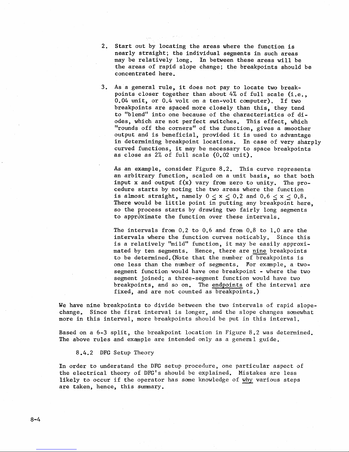
2.
Start
nearly
may
the
concentrated
3.
As a general
points
0004
breakpoints
to
odes,
"rounds
output
in
curved
as
As
an
input x and
cedure
is
There
so
to
out
by
straight;
be
relatively
areas
of
closer
unit,
or
are
"blend"
which
into
are
off
and
is
determining
functions,
close
an
as
2%
example,
arbitrary
output
starts
almost
the
would
process
straight,
be
appr6ximate
locating
the
rapid
here.
rule,
together
004
volt
spaced
one
not
the
corners"
beneficial,
breakpoint
of
full
consider
function,
by
noting
little
starts
the
the
individual
long.
slope
it
does
than
on a
more
because
perfect
it
may
scale
scaled
f(x)
namely
point
by
function
areas
In
between
change;
not
about
ten-volt
closely
of
switches.
of
the
provided
locations.
be
necessary
Figure
vary
the
two
0 < x <
i;
drawing
over
where
segments
pay
the
function,
(0.02
8.2.
on a
from
areas
putting
the
in
these
the
breakpoints
to
locate
4%
of
full
computer)o
than
this,
characteristics
This
it
is
used
In
case
to
space
unit).
This
unit
basis,
zero
to
where
0.2
and
any
two
fairly
these
intervals
function
such
areas
will
two
scale
they
effect,
gives
a
to
of
breakpoints
curve
represents
so
unity.
the
function
0.6
< x < 0
breakpoi;t
long
o
is
areas
be
should
be
break-
(i.e.,
If
two
tend
of
di-
which
smoother
advantage
very
that
The
sharply
both
pro-
8.
0
here,
segments
We
have
nine
change 0 Since
more
Based
The
In
the
are
above
order
likely
in
this
on
a
rules
8.4.2
to
electrical
to
occur
taken,
6-3
DFG
understand
hence,
The
intervals
intervals
is a relatively
mated
to
be
one
less
segment
segment
breakpoints,
fixed,
breakpoints
the
first
interval,
split,
and
example
Setup
theory
if
the
this
from 002
where
by
ten
segments 0 Hence,
determined.
than
the
function
joined;
and
and
are
to
divide
interval
more
the
breakpoints
breakpoint
are
Theory
the
DFG
of
DFG's
operator
summary.
the
function
"mild"
(Note
number
would
a
three-segment
so
on.
not
counted
between
is
longer,
location
intended
setup
should
has
procedure,
be
some
to
006
curves
function,
that
the
of
segments.
have
The
one
endpoints
as
the
and
should
only
explained.
knowledge
and
from
0.8
noticablyo
it
may
be
there
are
number
nine
of~akpoints
For
breakpoint
function
would
of
breakpointso)
two
intervals
the
slope
be
put
in
this
in
Figure
8.2
as a general
one
particular
Mistakes
of
why
to
1.0
are
the
Since
easily
this
approxi-
breakpoints
is
example, a two-
-
where
the
interval
of
changes
interval
was
the
have
rapid
two
slope-
somewhat
o
determined.
guide.
aspect
are
various
of
less
steps
two
are
8-4
Page 83

1.0
0.9
0.8
0.7
0.6
0.5
0.4
0.3
0.2
0.1
Y = f
~~
/
1\
(X)
OFF
\
\
\
2
/
1\
)
3
~
r
4
V
"6
~
0
7
I
J
/
J
V
V
'8
9
I
~
10
--l
.-0
FF
o
o
0.1
0.2
Figure 8
0.3
0.4
0.5
0.6
0.7 0.8
2.
Typical Ten-Segment Function
0
0.9
1.0
-
-
x
8-5
Page 84
Each
breakpoint,
changing
the
positive
duct.
slope
by
duced
point,
ure
tially
fect
breakpoint
OFF.
The
slopes,
sixth
larly
setup
In
value
·a
perfect
a
slight
shift
adjustment.
Each
of
adjusting
at a given
but
8.3
shows
setup
the
DFG
setup
but
breakpoint
for
procedure.
practice,
of
is
state;
the
function
x6• The
the
the
switch.
shift
negligible,
as
or
the
diode,
curve.
a
potentiometer
does
affect
the
function.
procedure
rather
other
the
function
in
or
"corner"
the
input
negative
when
The
point
is
slope
has
the
affect
The
value
tangent
values
adjusted
breakpoints.
pot
at
The
"corner"
)
f(x
5
but
in a DFG
voltage
direction,
it
starts
change
(the
no
affect
value
of
changing
incremental
at
that
line
is
arranged
of x and
by means
for a given
that
point,
will
·occur
in
a few
curve
moves away from.
more
to
conduct,
in
slope
slope
at
point,
represents
f(x).
This
at
x
w~en
cases,
for a given
pot).
on
the
subsequent
the
slope
slope
but
so
that
of
the
fact
segment
due
to
(Figure
setting
represents
and
more
increases
The
value
points
pot
introduced
does
affect
the
output
the
operator
Hence,
is
it
the
slope
the
does
the
fact
8.3)
f(x
neceSSl.tates
a
diode
the
origin,
diodes
segment
change
of
the
For
o
for
segment
at
the
with
function
pot
at
key
to
have
that
is
somewhat rounded,-
).
In
6
start
or
decreases
is
in
slope
function
example,
x5
value
the
does
the
understanding
an
effect
the
many
a
later
that
5 on a
does
not
value
fifth
diode
is
in
either
to
determined
intro-
at
not
at
the
SLOPE
observe
at
and
on
is
cases,.
"trinuning"
con-
the
that
Fig-
par-
af-
next
switch
the
simi-
the
the
not
and
this
8.4.3
Once
be
As
are
endpoints
the
straight
slope
setting
tion
fixed
In
to
f(x)o
the
case,
procedure
(Figure
is
and
read
an
example,
that
to
at 0 and-I.
setting
set
corresponding
the
marked
Setting
values
forward.
breakpoint
from a
directly
was
be
used,
and 9 breakpoints.
all
However,
procedure
makes
8.4),
TIME
of x and
The 580
table
on
consider
given
the
such a function,
breakpoints
it
is
f(x),
use
which
BASE
a
Ten-Segment
f(x)
variable
for
each
of
values;
the
DVM),
the
function
graphically
function
most
(x
values)
also
possible
and
continue
for
setting
of
the
DVM
is
in
the
AND.
MDFG
Function
are
tabulated,
segment.
first
and
then
in
is
tabulated
A
"+"
computer
first,
a
slope
and
right
INPUT.
DFG
has
The
adjust
set
in
Table
Figure
DFG
is
and
to
set
alternating
or a breakpoint
signal
half
the
function
potentiometers
DFG
setup
the
breakpoint
f(x).
8.1.
8.2.
at
operators
selector,
of
Note
11
points,
assumed,
then,
the
first
in
the
lower
setup
panel
This
and
will
set
and
is
that
.breakpoint
this
since
including
the
find
the
mannero
is
the
DFG
drawer.
is
for
adjusting
allows
x
(which
the
same
10
endpoints
it
easiest
function
x,
the
same 0 The
setup
quite
direct
may
func-
segments
the
£
are
values
then
In
either
panel
The
unit
set
8-6
Page 85
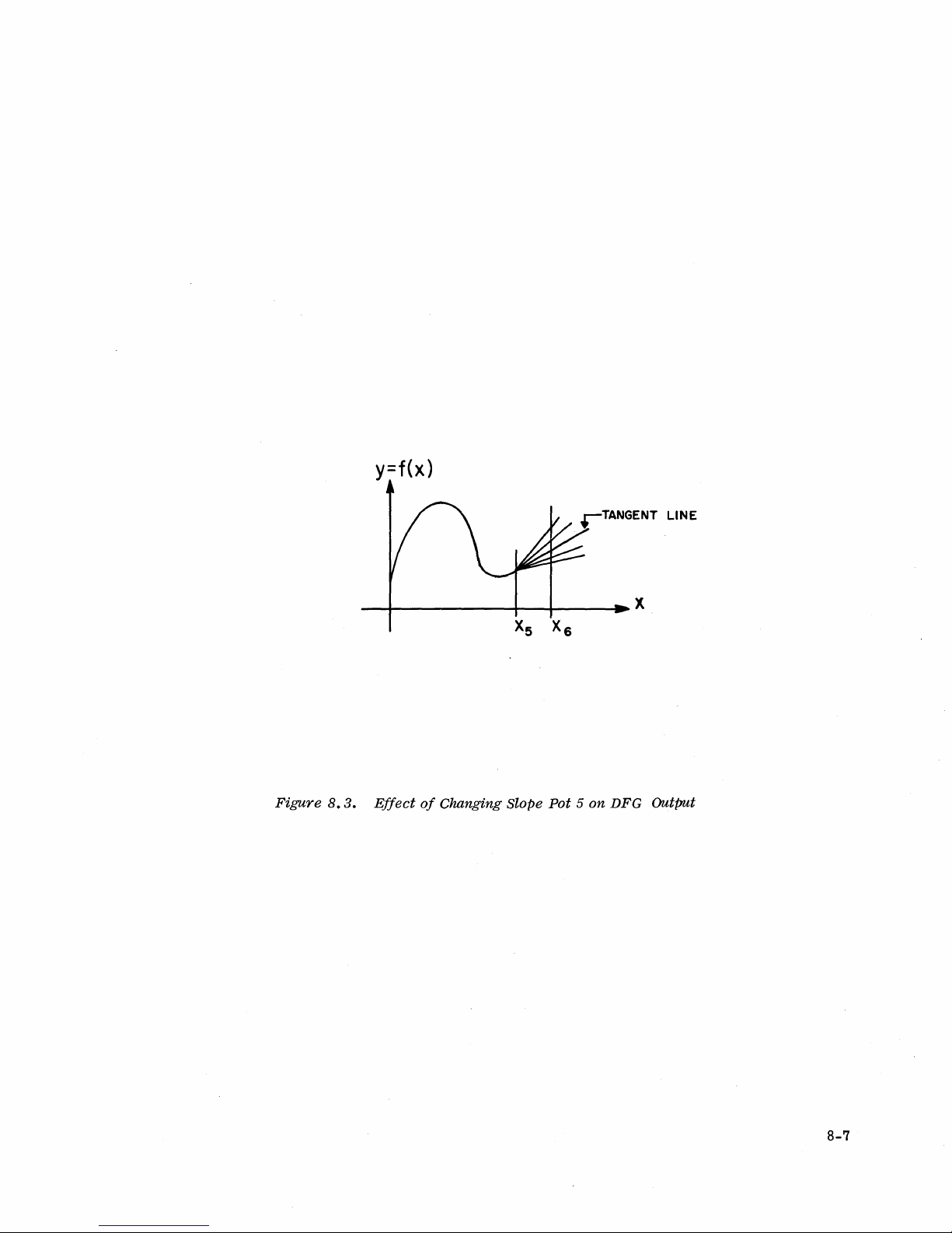
y=f(x)
Figure
__ ~ __________
8.3.
Effect
of
-+
__ ~ ____
Changing Slope
Pot 5 on
~x
DFG Output
8-7
Page 86
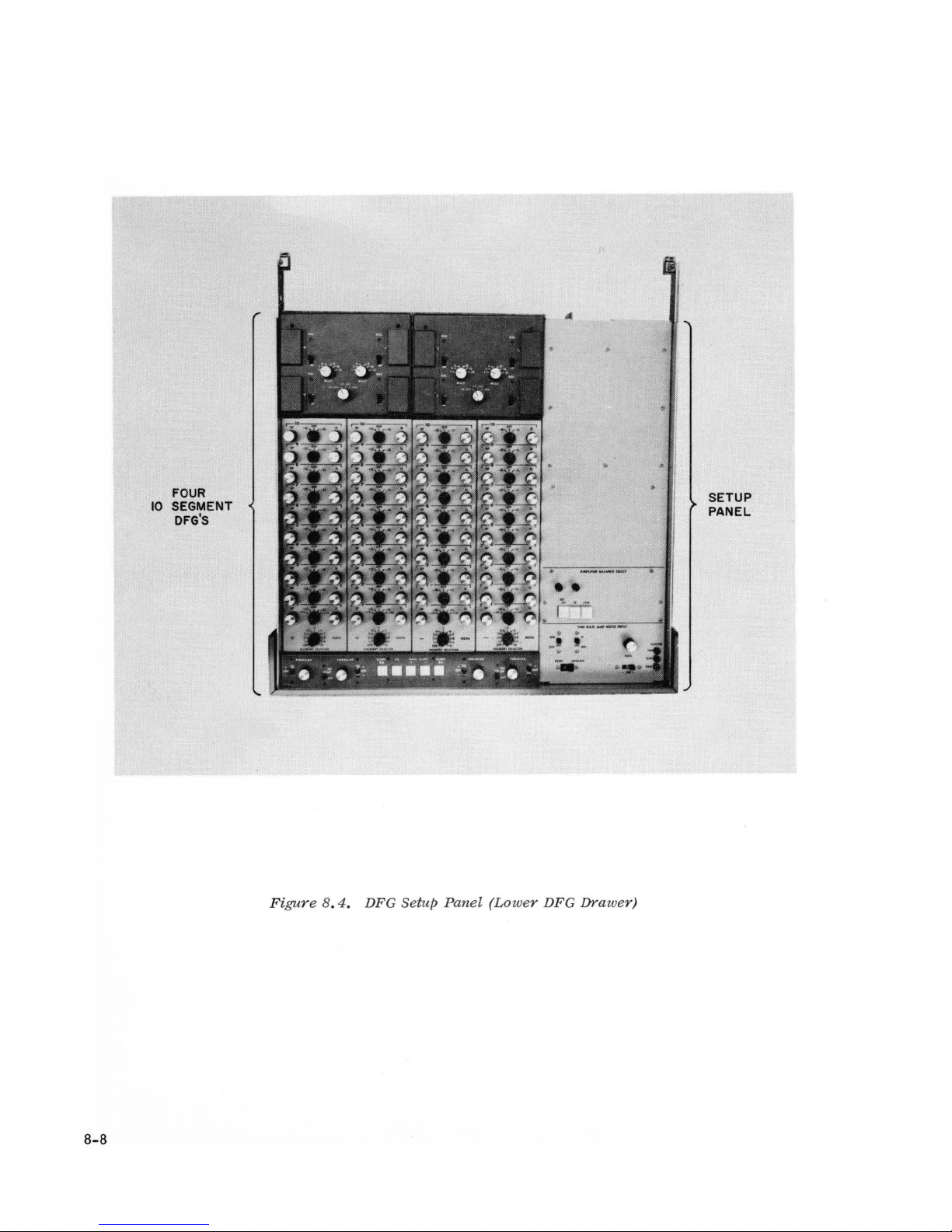
8-8
FOUR
10
SEGMENT
DFG'S
Fi
gure
8. 4.
DFG
Setup
Panel
(Lower
DFG
Drawer)
SETUP
PANEL
Page 87
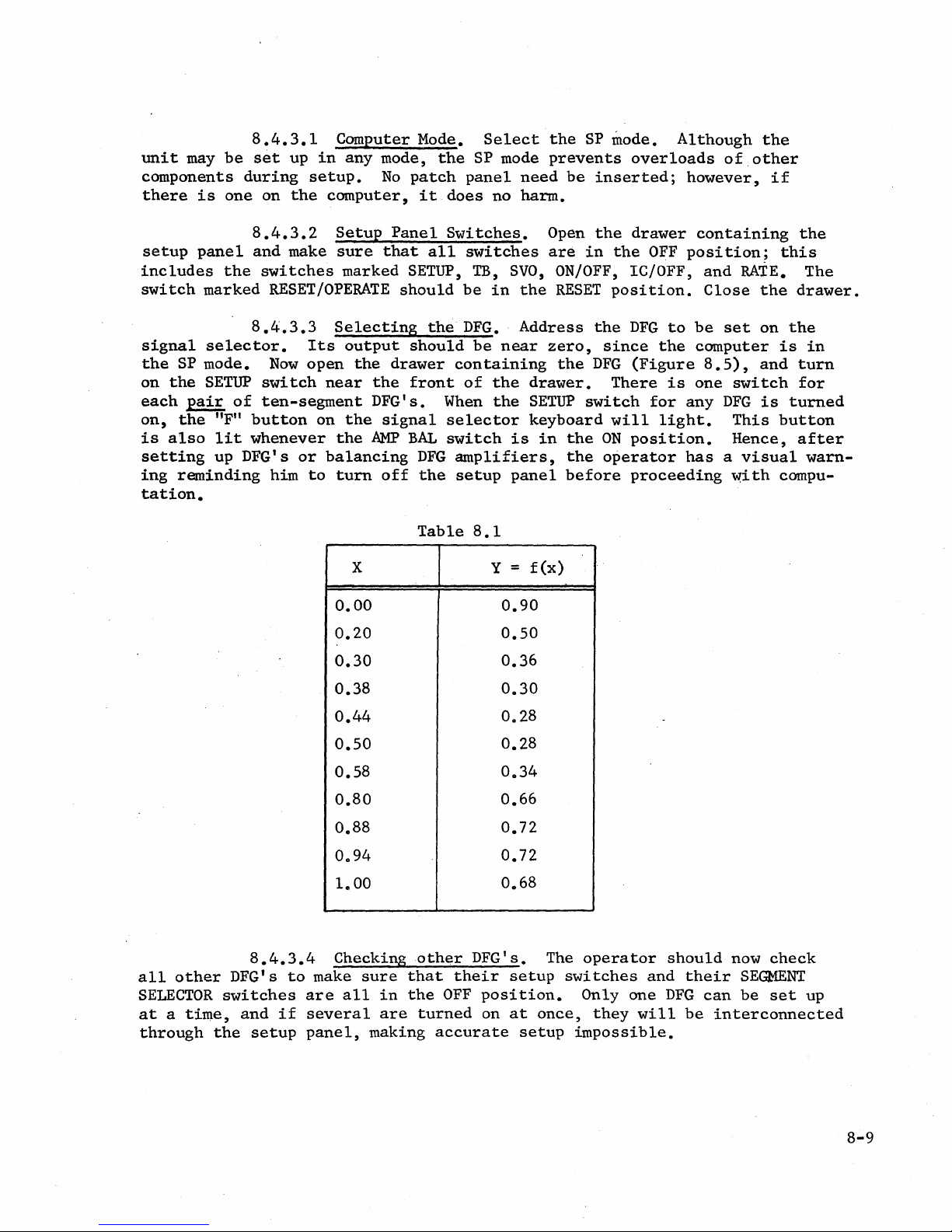
unit
may
be
components
there
is
one
8.4.3.1
set
during
on
up
the
in
setup.
Computer Mode.
any
mode,
No
patch
computer,
it
the
does
Select
SP
mode
panel
no harm.
the
prevents
need
SP
be
inserted;
mode.
overloads
Although
of
however,
the
other
if
setup
panel
includes
switch
signal
the
SP
on
the
each
on,
is
pair
the
also
setting
ing
reminding
tation.
8.4.3.2
and
the
marked
8.4.3.3
selector.
mode.
SETUP
of
"F"
button
lit
whenever
up DFG's
Setup
make
switches
sure
marked
RESET/OPERATE
Selecting
Its
output
Now
open
switch
ten-segment
or
him
to
the
near
the
DFG's.
on
the
the
AMP
balancing
turn
x Y =
0.00
0.20
0.30
Panel
that
SETUP,
should
should
drawer
front
signal
BAL
DFG
off
Table
Switches.
all
the
containing
When
selector
switch
amplifiers,
the
setup
switches
TB,
SVO,
be
in
DFG.
be
near
of
the
the
is
panel
8.1
0.90
0.50
0.36
Open
are
ON/OFF,
the
RESET
Address
zero,
the
drawer.
SETUP
keyboard
in
the
the
before
f(x)
the
in
the
position.
the
since
DFG
There
switch
will
ON
operator
drawer
OFF
IC/OFF,
containing
position;
and
Close
DFG
to
be
the
computer
(Figure
for
is
8.5),
one
any
light.
position.
has a visual
proceeding
RATE.
the
set
on
and
switch
DFG
is
This
Hence,
with
the
this
The
drawer.
the
is
in
turn
for
turned
button
after
warn-
compu-
all
other
SELECTOR
at a time,
through
the
8.4.3.4
DFG's
switches
and
if
setup
to
make
are
several
panel,
0.38
0.44
0.50
0.58
0.80
0.88
0.94
1.00
Checking
sure
all
in
are
making
other
that
the
turned
accurate
their
OFF
0.30
0.28
0.28
0.34
0.66
0.72
0.72
0.68
DFG's.
setup
position.
on
at
setup
The
switches
once,
impossible.
operator
and
Only one
they
will
should
their
DFG
can
be
now
check
SEGMENT
be
set
up
interconnected
8-9
Page 88
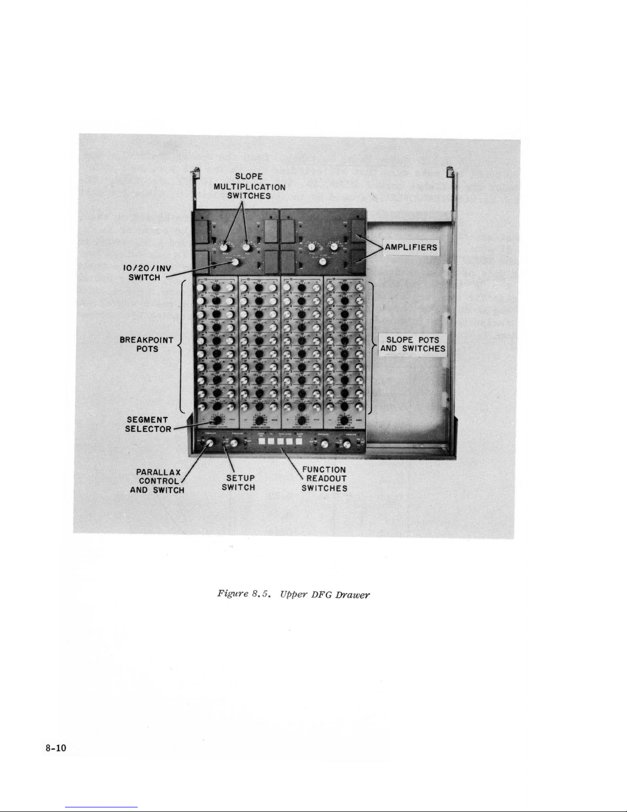
IO/20/lNV
SWITCH
BREAKPOINT
POTS
SEGMENT
SELECTOR
PARALLAX
CONTROL
AND SWITCH
I .
8-10
Figure
8.5.
Upper
DFG
Drawer
Page 89

on,
select
The
"10
arates
''MULT''
the
best
the
one
8.4.3.5
the
proper
SEG/20 SEG/INV"
the
unit
determines
setting
in
Figure
into
the
are
8.2, a setting
Preliminary
setting
on
switch
two
independent
maximum
covered
slope
in
Steps.
the
rotary
should
be
10-segment
change
Paragraph
of
"lll
Once
switches
in
the
per
8.4.4.
is
adequate.
the
DFG
SETUP
at
"10
SEG"
DFG's. The
segment;
For
the
switch
the
rear
posi.'t"ion,
switch
rules
for
function
is
turned
of
the
drawer.
which
sep-
marked
determining
such
as
.. , DFG
f(x),
being
starting
maxim1m
corresponding
is
momentary;
released,
Table
8.2
time.
the
values
final
values
Segment
Selector
OFF
2
3
4
5
6
7
8
9
10
OFF
set
x.
the
gives
The
804.3.6
up.
8.4.3.7
from x = 0
The
breakpoint
function
it
must
breakpoint
detailed
table
applies
of x and
of
x,
X
Value
000000
1.0000
Slope
Switches.
Setting x and
and
value
'Talue,
be
held
~e
information
to
any ten"!'segment
f(x)
have
which
Set
This
must
X on
Point
None
BP2
BP3
BP4
BPS
BP6
BP:]
BP8
BP9
BPIO
None
Turn
f(x).
proceeding
is
read
depress
down
x
is
the
while
again
on
been
be
Table 8 ..
left
zero
and
2
Then Hold
this
·While
PX
SLOPE
SLOPE
SLOPE
SLOPE
I
SLOPE
SLOPE
SLOPE
SLOPE
SLOPE
+FINAL
all
Now
out
directly
appropriate
setting
displayed.
which
function
blank,
one.
Down
Button
Setting
RO
RO
RO
RO
RO
RO
RO
RO
RO
SLOPE
slope
set
from
switch
except
Y
switches
up
the
the
on
the
f(x).
to
with
Set
Pot
PARALLAX
values
origin
DVM;
switch.
When
depress
positive
for
the
Y on
and
SLl1(
.
'SL2
SL3
SL4
SL5
SL6
SL7
SLB
SL9
SLlO
off
of x and
toward
to
Each
the
at
initial
This
Switch
for
the
read
switch
switch
any
inputs;
the
the
is
given
and
Y
Value
+CS
-
position,
*Use
not
+SL
-
position
o
8-11
Page 90

first
setting
and
on
Paragraph
ten-segment
is
skipped
8.4.3.8
last
setting,
the
previous
8.4.2.
operation.
(see
The
Note
left-hand
Pattern
the
slope
also
This
column
value
pot.
that
means
of
Settings.
of y at
The
BP
pot 1 is
that
in
Table
any
point
reason
not
position
8.2).
Notice
for
this
set;
1 on
that
is
determined
is
it
is
the
except
explained
not
used
SEGMENT
for
the
by
the
in
in
SELECTOR
pot
and
when
the
f(x)
setting
+SL
value.
affect.
To
determine
depressing
segment
this
point.
If
the
desired
mentoff,
if
it
is
then
the
to
memorize
if
the
output
In
any
case,
value
If
set
tion,
again,
remain
ly.
the
should
the
switch
to
zero;
from
checking
essentially
This
slope
previously
8.4.3.9
switch".
the
or
-SL
If
whether
the
turned
Tu~ng
then
desired
-SL
position
this
moves
it
change
has
give
8.4.3.10
the
is
because
at
the
set
Slope
Each
function
position,
the
switch
to
readout
off.
This
the
function
the
switch
to
decrease
rule,
in
is
the
in
no
effect
it
a few
origin
the
funtion
constant,
the
previously
function
Switch
slope
value,
and
is~the
use
the + or -position,
button.
value
segment
value
should
should
but
the
be
simply
wrong
direction
the
right
on
turns
Trimming
outward,
values
but
value
set
value.
Position.
pot
has a slope
the
operator
then
adjusts
OFF
This
displays
will
not
on
will
is
more
be
turned
the
function
used.
turn
direction,
of
change
direction
the
function
and
repeat
Adjustments.
the
operator.
f(x).
the
function
at a given
breakpoint,
the
(center)
be
increase
positive
to
value
Some
the
switch
that
when
value,
The
breakpoint
causing a small
The
table
switch
first
pot
to
position,
leave
the
function
equal
to
or
than
the
+SL
(make
computer
on
the
switch
is
important;
the
the
the
ON/OFF
Having
should
now
breakpoints,
values
says
to
immediately
turns
obtain
on
the
the
the
the
switch
value
the
desired
decrease
the
value
position.
it
more
operators
in
either
should
switch
slope
is
pot
process.
set
up
the
go
through
once
may-
have
is
set
by
shift
"set
y on a
to
its
switch
correct
pot
has
off
with
value
this
value.
with
the
Conversely,
negative),
prefer
direction;
be
reversed.
the
function
turned
is
probably
ono
entire
the
set,
should
changed
changing
in
the
left;
to
nq
while
the
at
seg-
not
functable,
slight-
The amount
spacing
(10
to
shift
moved by a
in
the
outward.
since
in
function
be
correct
ming
adjustments
of
of
breakpoints,
20
millivolts),
is
negligible.
series
same
The
the
breakpoints
to
this
order
trimming
values
within
needed.
8-12
shift
of
trimming
as
the
are
0.0002
depends
but
it
and
rarely
However,
original
process
do
not
required.
to
upon
is
generally
greater
if
desired,
adjustments
setup -starting
goes
much
have
to
After
000005
the
faster
be
set
trimming,
unit;
nature
about
than
most
These
o
again,
rarely
of
the
0.0010
0.0050.
of
this
adjustments
at
than
the
and
most
is a second
function
to
In
many
effect
the
origin
original
only
function
0.0020
cases,
may
should
small
values
set
and
the
unit
be
be
and
working
setup,
changes
of
this
re-
made
will
trim-
Page 91

of
output
versus
documentation.
580
DFG
setup
sweep
priate
ON
from
ence
the
To
tion.
menting
the
and
for
plotter
switch
-Reference
downwards,
IC.
To
make. a
The
will
plot
turn
is
the
the
ON,
plot,
rate
8.4.3.11
Such a
panel
input.
input
contains
Plotting.
should
plot
Slide
connections
and
set
the
upwards,
put.
the
RATE
start
put
of
the
the
sweep
the
switch
sweep
produce a setting
completed,
OFF/ON
put
switch
at
IC
turn
the
OFF.
Once
be
made,
may
be
made on
a
built-in
out
the
upper
the
terminals
and
RATE
the
RATE
switch
at
x =
to
0,
marked
is
determined
that
does
RESET/OPERATE
the
function
which
ramp
switches
switch
Il_";
turn
serves
the
integrator
DFG
drawer,
on
to
this
the
580
the
appropriately.
tf+".
reverses
IC
switch
RESET/OPERATE
by
the
RATE
not
overdrive
switch
is
set,
as
part
without
to
and
right.
To
to
the
pot; a little
the
to
the
a
continuous
of
the
problem
repatching.
provide a smooth
make
sweep from
both
Turn
the
on
To
the
approthe
sweep
+Refer-
rate
OFF.
OPERATE
posi-
experi-
plotter.
RESET
When
position
plot
The
OFF/
and
8.4.4
During
cannot
(ten
thing
pot.
the
be
times)
to
Also,
Assuming
insufficient
For
each
it
can
introduce;
clockwise.
one
segment,
tion
slope
The
(see
changes
slope
resistance
steep
or
essary.
tation
is
proportion
(3 x 32).
Insufficient
above
procedure,
obtained.
and
the
do
is
to
check
make
that
no
sure
such
slope.
segment
there
this
On
the
assuming
Paragraph
as
great
multiplication
on
the
output
sharply
There
~.O
to
curving
is
also a limitation
if
the
the
setting
Slope
it
may
If
the
slope
function
the
error
is
is
Table
slope
an
the
value
8.2
has
upper
amount
580, a maximum
the
slope
8.4.3.5).
as
32.
switch
multiplication
Other
works
amplifier,
functions,
MULT
switch
on
this
happen
pot
still
and
polarity
been
made,
limit
produced
slope
positions
thus
a
on
is
in
switch,
that a particular
is
rotated
has
not
make
sure
switch
the
problem
to
the
with
change
of
switch
of
by
changing
providing
position
the
the
initial
"1"
so
that
other
position,
to
the
been
you
are
is
in
amount
the
1.0
this
the
greater
than
slape
the
end
of
reached,
setting
the
right
is
probably
of
slope
slope
may
be
is
in
the
switch
effective
gain.
"1"
fICO).
and
maximum
function
its
the
the
position.
change
pot
fully
obtained
"1"
allow
feedback
For
may
be
This
it
goes
value
value
travel
first
right
one
of
with
posifor
every
nec-
limi-
up
is
that
in
96
The
effective
high
output,
is
cular
A
ceed
settings
such
as
not
desirable
function.
conservative
to
making
bandwidth
set
try a setting
number
of
requirement
the
false
prior
resolution
a
small
accurate
are
to
procedure
function
of 2 and
starts,
to
motion
setup
degraded
use
any more
try
and
setup
of
is
until
again.
is
the
slope
of
the
difficult.
at
high
gain
to
set
insufficient
some
methods
desirable.
pots
pot
produces a large
gain
than
the
switch
However,
of
decreases
Also,
setting.
necessary
initially
slope
this
estimating
with
electrical
For
in
is
encountered,
procedure
the
higher
change
characteristics
this
reason,
generating
at
"1",
may
lead
maximum
gain;
in
and
then
the
a
parti-
pro-
to
slope
at
it
a
8-13
Page 92

Such
the
breakpoint
lows:
an
estimate
may
locations
1.
Locate
either
2.
Estimate
triangles
3.
Form
the
required,
Note
magnitudes
mum
points
4.
Divide
the
the
case"
what
slope
as a starting
be
easily
have
visually
the
the
the
difference
maximum
between
that
positive
near
the
number
average
region.
greater,
change.
obtained
been
positive
slope
or
counting
negative
in
subtracting
are
added.
and
each
total
of
breakpoints
slope
The
since
However,
point.
determined.
the
points
or
of
the
squares
between
slope.
the
two
negative
other
slope
change
slope
not
from a
where
negative
curve
the
points
two
If
there
slopes,
where
change
in
per
actually
all
segments
this
graph
The
procedure
the
direction).
at
these
on
the
graph.
maximum
This
is
where
slopes
are
of
several
choose a pair
the
slope
between
this
interval.
breakpoint
required
will
estimate
of
the
slope
points
positive
the
total
maximum
opposite
difference
these
in
the
may
have
is
a good
function
is
is
steepest
by
slope
slope
sign,
points'of
of
two
points
This
"worst
be
the
one
as
fol-
drawing
slope
occurs.
such
is
gives
some-
same
to
once
(in
and
change
the
maxl-
large.
by
use
8.4.5
As
an
example
This
serted
ly
by
late
curve
in
observing
the
procedure
Breakpoint
There
$ince
gion,
are 4 relatively
the
the
region.
MENT
OFF,
SELECTOR
2,
3,
skipped.
The
greatest
slope
tion
occurs
of
the
Graphical
about
11.S.
average
able
5e5,
Since
slope
whether a slope
breakpoints
Example
of a function
was
initially
the
X-Y
plotter.
the
function.
as
well
as
location
function
nine
Note
available
that
position
4,
••• , 9,
positive
just
past
graphe
determination
and
the
there
change
will
require
of
Slope
drawn
plotter,
Thus
was
the
of
slope
determined
straight
appears
breakpoints
the
breakpoints
that
10,
slope
the
of
negative
are
three
per
segment
multiplier
greater
Amplification
requiring
free-hand
Breakpoints
not
the
curve
amplification.
portions
to
curve
will
be
OFFo
As
occurs
first
the
peak;
slopes
slope
breakpoints
is
of 4 will
slope
slope
on a
and
DVM.
offers
by
following
and 3 relatively
about
were
have
been
used
in
mentioned
at
the
these
indicates
about
-6.
between
11.5/3
change
amplification,
sheet
function
Hence
of
there
graph
values
was no
a good example
the
rules
the
same amount
equally
marked
setting
distributed
according
them. The
previously,
left
facts
The
or
3.9.
be
adequate,
than
side;
the
are
that
the
difference
these
It
others
obvious
two
is
since
see
paper
were
need
~f
graphical
in
Paragraph
"curvy"
in
each
to
position
greatest
positive
in
points,
somewhat
some
However,
o
Figure
and
set
to
portions.
curve
three
the
pattern
1
negative
by
inspec-
slope
slopes
the
question-
of
8.6.
in-
direct-
tabusetup
8.4.1.
per
SEG-
goes:
is
is
these
it
re-
is
may
8-14
Page 93

Y
1.0
0.9
=f(X)
U
OFF-
0.8
0.7
0.6
0.5
0.4
0.3
0_2
0.1
o
I
I
j
!I
•
I
o
Figure
/
0.1
r
8.
I
I
2
0.2
6
4
N
\
\
,
0.3 0.4
Typical
/5
\ J
L/f
'I
7
6
0.5
Function
8
'\
V
/
il
0.6
Requiring
/9
'"
0.7
0.8
Slope
Amplification
Ie
'\
\
0.9
i\
\
/OF
\
t
1\-
1.0
F
x
-
8-15
Page 94

be
possible
conservatively
As
might
The
be
smallest
(About 00025
value
tion
(8)
is
changed,
and
previously
doubling
ever,
by
the
the
the
breakpoint
slope
to
get
by
specified
expected,
value
obtainable
unit.)
the
setup
it
set
function
gain
will
amplification
with
there
The
was
is
necessary
value,
double
settings
4,
on
most
was
slope
repeated.
switch.
especially
since
DFG'so Hence a
difficulty
was
about a quarter-inch
multiplier
in
switch
Note
to
go
back
starting
the
entire
do
not
with
have
function
to
setting
that
to
the
be
the
the
slope
setting
the
above
was
set
when
the
beginning
PARALLAX
up
to
reset;
they
rating
of
value
to
slope
setting,
that
4 was
the
the
and
pointo
are
is
somewhat
tried.
at
point
curve.
next
higher
amplifica-
reset
every
since
How-
unaffected
50
With a slope
was
observed
setup
was
completed
tinguishable
that
the
maximum
necessary.
80406
At
this
setup
position
ment
segment
Whenever
0),
The
in
Figure
Note
point
point
control
point,
procedure
on
functions
functions
the
then
the
additional
807,
that
is
is
since
the
set
for
setting
in
setting
of
8~
the
function
indicated
from
the
original
deviation
Eleven-Segmen~
the
reader
calls
the
segment
(see
Paragraph
0
function
function
may
segment
may
for
ignoring
selector.
to
be
be
is
horizontal.
was
Functions
generated
generated
and a corresponding
the
value
by
adjusting
adjusting
first
at
the
the
segment
or1g1n.
the
function
setup
proceeded
values.
that
the
hand-drawn
about
be
0.3%.
wondering
this
This
8.4.6)
and,
table
is
horizontal,
In
slope
at
value
A
continuous
plotted
curve
No
what
breakpoint
breakpoint
under
is
initially
with
An
fact,
example
of
the
at
eleven
values
since
previous
breakpoint
smoothly.
plot
function
over
most
trimming
"Breakpoint
pot
and
is
usable
certain
horizontal
segments
of
such a curve
is
given
the
value-
the
value
breakpoint,
number
No
difficulty
was
of
made
virtually
its
after
length,
adjustments
1"
is
its
corresponding
for
twenty-seg-
conditions,
(that
instead
in
Table
at
the
at a given
there
one
for.
is
first
o
the
indis-
were
for
is,
of
ten.
given
803.
break-
is
and
The
eleven-
f'(O)
break-
no
=
Segment
Selector
OFF
1
2
3
4
5
8-16
x
0.00
0.06
0.12
0.18
0.34
0.40
f(x)
0.33
0.33
0.36
0042
0.72
0.80
Table
Segment
Selector
8.3
6
7
8
9
10
OFF
x
0.46
0.52
0060
0.70
0.84
1000
f(x)
0.84
0.84
0.82
0.76
0.60
0.32
Page 95

Y=f{X)
1.0
"
0.9
0.8
0.7
0.6
0.5
OFF
0.4
4~
0.3
T
0.2
0.1
I
o
o
Figure
I
It
4
I
/ \
/
j
(t
~
0.1
0.2
0.3
8.
7 Initially Horizontal
0.4
....
v.
~
....
~~
.....
.
-....
~
I
7
0.5
~
0.6 0.7
Eleven-Segment
9
I
10
'\
~
"
OFF
0.8
Function
~
~
0.9
1.0
x
-
-
8-17
Page 96
The
setup
lowing
The
reason
a
CENTER
pot
is
ciated
the
input
set
the
an
additional
used
mines
procedure
exceptions:
1.
20
for
SLOPE
used
in
with
to
it.
the
initial
as a slope
the
value
is
Position
used
set,
SLOPE
without
should
the
PARAIJ.,AX
to
interaction
The
slope
than
this
this
pot;
feature
it
manner,
Electrically,
output.
slope.
segment
pot
for
of
the
similar
1 on
for
setting
the
function
RO
button,
disturbing
be
equal
switch
the
~S
is
this
If
Hence,
becomes
the
function
as
the
breakpoint
but
to
control),
with
for
position.
is
that
pot
there
the
f'(O)
by
available.
extra
at
for
any
SEGMENT
value
can
there
the
rest
the
value
plus
the
next
BPl
is
the
slope
that
sets
is
no
diode
pot
simply
=
0,
then
adding
one
segment.
the
~
other
function,
SELECTOR
10
Once
be
read
is
no way
of
the
of
x = 0
or
minus a small
setting.
put
in
pot
the
slope
and
provides
there
more
The
CENTER
The
setting
breakpoint.
is
not
the
out
by
to
adjust
function.
(previously
the
+SL
for
segment 1 is
at
hence
no
linear
is
no
pot,
(breakpoint
SLOPE
of
with
the
skipped
breakpoint
depressing
this
The
increment
position,
x =
O.
breakpoint
gain
need
for a pot
pot
can
this
pot
two
It
o
has
value
value
set
rather
actually
When
from
pot
now
deter-
fol-
is
been
the
by
due
the
asso-
to
1)
be
8-18
8.4.7
The
above
inputs
only.
generating
are
equipped
stalled
The
in
setup
starting
-1.0000.
SLOPE
for
button,
determining
Negative
procedure
The
functions
with
any
proportions.
procedure
from
zero,
The
value
rather
output
an
the
Inputs
applies
values,
with
equal
for
the
work
at
away from
this
than
polarity
to
the
negative
number
-DFG
last
+FINAL
of
the
+DFG;
however,
inputs,
of
either
is
essentially
the
origin
endpoint
SLOPE.
slope
this
may
the
type;
is
The
switch
type
be
-DFG
the
toward
ready
rule'
of
DFG
of
either
is
used.
however,
same
the
by
depressing
given
should
accepts
polarity.
they
as
for
final
in
Paragraph
be
reversed.
positive
Most
computers
may
be
the + type;
value
the
For
in-
of
-FINAL
8.4.3.9
Page 97
8.4.8
Twenty-Segment
Functions
Provision
is
twenty-segment
then
available
tion
of
over
It_If
is
be
twenty
The
of
the
the
Similarly,
switch
and
in
CENTER
central
Segment
can
serve
more
segments,
both
(both
"+"
are
used
the
"+"
put
in
any
bre~kpoints
PARALlAX
them
is
output
other
1)
determine
input
resistor;
twenty-segment
SLOPE
slope.
Functions".
polarities.
or
type
simply a bias
o
should
the
made
for
unit.
for
independent
The
either
or
the
both
"_II)
together.
and
the
position,
in
controls
In
twenty-segment
be
turned
controls
the
like
operation.
control
This
may
capability
operating
unused
a
pair
output
use
of
two
purposes:
generation
For
the
former
are
used
'In
most
second
so
the
interval
on two
together;
connnon
is
that
it
connected
the
adding a constant
operation,
offo
marked
slope
the
CENTER
at x ='0.
PARALLAX
However,
be
used
as
is
of
ten-segment
amplifier
as
an
inverter.
increased
of
functions
purpose,
for
arrangement,
If_If
type.
is
possible
0 ~ x ~ 1.
DFG's
(positive
only
SLOPE
This
controls,
unlike
an
ordinary
described
~rom
two DFG's
the
However,
to
perform
one
(i.e.,
slope
one
the
segment
in
Paragraph
of
DFG's
the
as a single
second
Twenty-segment
accuracy
an
latter,
the
input
of
one
first
through
the
either
obtain
of
the
is
of
PARALLAX
(for
the
same
or
negative)
these
~S
position
determined
these
control,
w~en
controls
not
804.6,IfEleven-
DFG
that
same
u+"
and
DFG
in a pair
type
example)
function,
voltage
by a
is
redundant
needed
is
opera-
the
ranges
type
one
may
is
on
pot
the
use
each
to
needed,
slope
for
In
the
case
of a DFG
be
given
What
f(x)
tion
cannot
no
diodes
input.
i.e
o
on
either
these
pass
correct
is
desired
at
values
be
The
,
the
two
the
values
to
the
problem
is a straight-forward
all
breakpoints.
of
the
set
directly
are
conducting,
PARALLAX
value
when x =
the + or
parameters
line
through
at
two
the
the
with
positive
of
setting
If
breakpoints
and
independently.
and
pot
allows
O.
The
-DFG,
allows
completely
any two
two
breakpoints
and
the
there
is
nearest
the
output
setting
CENTRAL
setting
characterize
points;
negative
values
method
no
breakpoint
zero
Over
is
the
SLOPE
i.e
,
o
(one
positive,
in
of
inputs,
the
setting
(one
the
some
interval
the
at
x =
positive,
interval
simply a linear
y-intercept
pot,
the
slope'of
the
line,
they
can
which
they
be
one
of
set
negative)o
thought
values
0,
containing
function
this
is
Slope
this
can
to
around
then
one
function,
line.
be
give
should
zero.
of x and
the
func-
negative)
zero,
of
the
Pot
1
Since
set
to
the
8-19
Page 98

However,
the
interaction;
not
exist
value
effect
if
necessary.
To
set
and
tabulate
should
breakpoints
interval.
does
of
the
be
anywhere
not
the
values
calculated
on
Of
drawing a line
x = 0
rected
and
for
at
the
relation
each
pot-setting
disturb
"diode
at
f(O),
either
course,
connecting
one
of
other
between
except
previous
curvature"
the
two
even
by
though
linear
side
the
the
two
breakpoint.
these
affects
at
this
one
settings,
which
breakpoints
this
interpolation
of
zero,
interpolation
these
points.
breakpoints,
two
pot-settings
both
values.
Interval.
except
is
easily
containing
is
not a breakpoint.
between
since
the
can
Once
they
curve
be
the
should
done
has a relatively
This
Setting
for
the
taken
care
zero,
the
is
straight
graphically
values
automatically
interaction
any
other
small
first
The
values
of
by
value
secondary
calculate
at
over
simply
have
been
large
does
function
"trinnning"
of
f(O)
the
this
by
set
at
be
cor-
Since
tion,
there
one
of
is
no
the
lows 9 breakpoints
The
operator
where
As
it
an
example,
regions
relatively
of
the
graph
gion
tra"
TRAL
lies
breakpoint
SLOPE,
sulting
SELECTOR
the
table.
In
setting
and
put
tion.
Since
(the
put
able
r'ight)
Address
both
one
amplifier
for
should
Paragraph
quate
should
do
not
for
also
set
.where
may
is
needed
consider
it
straight
and
mostly
and
breakpoint
positions
the
function,
the
rotary
the
DFG's
whose
address
(the
use
as
be
8.4.4
this
function;
be
set
function
need
two
pots
to
be
put
this
most.
curves
One.
o
another
on
the
on
the
BPI on
tabulation
for
switch
appropriate
are
connected
one
an
inverter.
set
to
indicates
to
1.
values
for
two
can
used
tenth
the
rather
of
in
positive
+DFG.
the
+DFG
each
first
at
ends
ending
10
that
hence,
Set
at
CENTRAL
be
used
on
one
breakpoint
function
sharply,
the
curved
the
positive
side,
Hence,
is
is
given
segment
turn
the
rear
output
to
in
-6)
in
-7)
Its
A
quick
a
slope
the
all
this
SLOPE
for a regular
side
of
in
Figure
separated
regions
half.
it
appears
BPI on
used
as a regular
in
Table
are
given
all
slope
of
the
amplifier
the
first
that
should
disconnected
slope
multiplier
calculation
multiplier
slope
breakpoints
time
0
pots
zero,
on
either
8.8.
lies
Since
the
-DFG
8.4.
on
the
switches
drawer
on
amplifier,
be
addressed.
based
of
multiplier
(positive
in
twenty-segment
breakpoint.
and
10
on
side,
This
function
by
regions
in
the
the
third
advisable
is
used
breakpoint.
Note
figure,
off
to
the
the
SIGNAL
it
is
from
the
switch
on
(the
the
unity
switch
and
This
the
other
depending
where
negative
curved
to
put
for
the
The
that
the
as
well
for
both
"20
SEG"
SELECTOR.
this
amplifier
The
other
DFG,
and
one
techniques
is
probably
on
the
negative),
opera-
al-
o
upon
has
three
it
is
half
re-
the
"ex-
CEN-
re-
SEGMENT
as
in
DFG's
posi-
out-
is
avail-
on
the
of
ade-
left
but
Only
time 0 When
function
that
the
8-20
one
the
"OFF"
SEGMENT
setting
values
SEGMENT
position
NOTE
SELECTOR
either
on
one
SELECTOR
o
should
breakpoints
of
the
on
be
DFG's,
the
other
on
at
or
ensure
one
a
is
in
Page 99
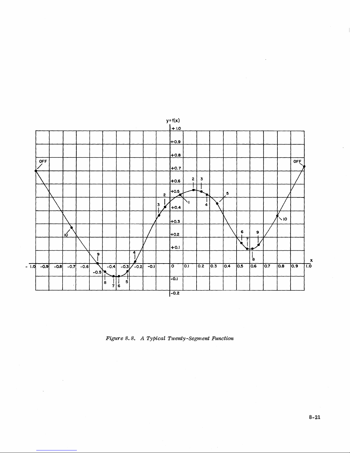
/
OFF
y=f{x)
+1.0
+0.9
+0.8
+0.7
OFF
.......
I
1.0
\
\
-0.9
\
\
-0.8
1\
16\
-0.7
\
-0.6
I\i
""\
-0.5
-0.4
~-
I
11
8
7 6
Figure
-0.3
_A
5
8.8.
V
V-0.2
I
/
V
I
-0.1
A
Typical
+0.6
+O~
2
/
~y
+0.4
'1
)
+0.3
+0.2
+0.1
0
-0.1
-0.2
Twenty-Segment
2 3
~
'-I
0.1
~
J\C
0.2
0.3
Function
..,,5
,
l\
0.4
\
~
0.5
6
I
9
!/
Y
~
0.6 0.7
/
I
"
0.8
/
10
/
/
/
0.9
x
1.0
8-21
Page 100

Table
8.4
x
-1.00
-0.74
-0.54
-0.48
-0.42
-0.38
-0.32
-0.26
-0.08
-0.04
0.00
+0.08
+0.18
+0.24
+0.28
f(x)
+0.70
+0.28
0.00
-0.06
-0.10
-0.10
-0.06
+0.02
+0.38
+0.44
+0.47
+0.53
+0.56
+0.55
+0.52
+0.36 +0.46
OFF
10
9
8
7
6
5
4
3
2
OFF
1
2
3
4
5
SEGMENT
-DFG
(Both
+DFG
SELECTOR
SEGMENT
Position
SELECTORS
Off)
Set
both
put
the
positive
MENT
SELECTOR
point.
SLOPE
be
If
RO
correct.
it
is
happens,
at
these
from
the
the
SEGMENT
values
+0.54
+0.58
+0.16
+0.12
+0.62 +0.12
+0.66
+0.80
+1.00
SEGMENT
+DFG
SEGMENT
+0.14
+0.36
+0.74
SELECTOR
SELECTOR
breakpoint.
in
position
(Note
button
not,
the
is
then
determine
switch
depressed,
the
the
breakpoints,
origin,
and
SELECTOR
on
the
other.
Turn
three
correct
set
then
for
10
OFF
switches
in
this
SEGMENT
2
to
read
positions,
the
tabulated
f(O)o Once
the
function
do
the
one
DFG
6
7
8
9
to
the
position
the
as
function
same
for
when
setting
HOFF"
1,
and
SELECTOR
value
tabulated
value
values
proper
values
the
position
set
off
at
the
in
at
are
on
the
+DFG.
either
the
and
first
Table
this
not
collinear;
values
-DFG,
Remember
breakpoints
and
set
f(O).
value
put
the
at
other
negative
8.40)
When
breakpoint
if
have
been
working
to
or
the
break-
should
this
obtained
outward
turn
function
Then
first
SEG-
the
off
8-22
 Loading...