


MSP430F5132 Experimenter’s Board (F5132EX)
F5132EX User’s Guide Rev. 1.1 – Apr./2016 Page 1
User Guide
EA Electronics
8 Maple St. Ajax, ON
Canada
www.eaelec.com
Introduction
The Texas Instruments MSP430™ family of ultra low-power micro-controllers consists of several
devices featuring different sets of peripherals targeted for various applications. The architecture,
combined with five low-power modes, is optimized to achieve extended battery life in portable
measurement applications. The device features a powerful 16-bit RISC CPU, 16-bit registers, and
constant generators that contribute to maximum code efficiency. The digitally controlled oscillator (DCO)
allows wake up from low-power modes to active mode in less than 5 μs.
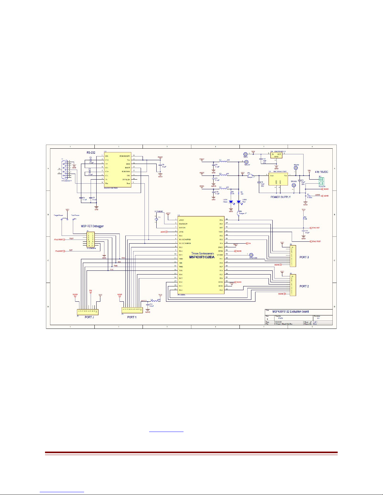
Schematic
The Experimenter’s board provides the micro-controller, an RS232 serial port, a JTAG header for
software debugging, 2 low-dropout voltage regulators and a prototyping area. The standard microcontroller is the MSP430F5132 in the 38 pin TSSOP package. This chip features 8K of flash and 1K of
SRAM memory. The board is also available with the MSP430F5172 (32K flash, 2K SRAM) for
applications which require more memory.
The JTAG header (J1) is used to connect the MSP-FET430UIF. The MSP-FET430UIF is and incircuit programming/debugging tool made by Texas Instruments. It is not included with the F5132EX but
can be purchased from any large distributor of TI products such as Digi-Key. The Code Composer Studio
IDE can be downloaded for free from www.ti.com and provides the assembler and C compiler.
F5132EX User’s Guide Rev. 1.1 – Apr./2016 Page 2
The JTAG Header

Prototyping Area
The prototyping area has pads for 3 TSSOP devices (up to 20 pins), 3 SOIC devices (up to 20
pins), 4 DPAKs, 4 SOT-23, a 2mm header (10x2), a 1.5mm header (1x6), various DIPs and .1” headers,
and many 2 terminal devices (both surface mount and through hole); such as resistors, capacitors and
diodes. The port pins on the MSP430F5132 are broken out to SIP pads at the edge of the prototyping
area. Note: the following port signals are not bonded out on the 38 pin TSSOP package: ports 3.4, 3.7,
J.4 J.5 and J.7. Pins J.0 thru J.3 are not available when using the JTAG debugger.
Top View
GPIO Port Breakout Connections
Port 1 Port 2 Port 3 Port J
Pin 1 AGND Pin 1 DGND Pin 1 DGND Pin 1 DGND
Pin 2 P1.0 Pin 2 P2.0 Pin 2 P3.0 Pin 2 PJ.0*
Pin 3 P1.1# Pin 3 P2.1 Pin 3 P3.1 Pin 3 PJ.1*
Pin 4 P1.2# Pin 4 P2.2 Pin 4 P3.2 Pin 4 PJ.2*
Pin 5 P1.3 Pin 5 P2.3 Pin 5 P3.3 Pin 5 PJ.3*
Pin 6 P1.4 Pin 6 P2.4 Pin 6 NC Pin 6 NC
Pin 7 P1.5 Pin 7 P2.5 Pin 7 P3.5 Pin 7 PJ.6
Pin 8 P1.6 Pin 8 P2.6 Pin 8 P3.6^ Pin 8 NC
Pin 9 P1.7 Pin 9 P2.7 Pin 9 NC Pin 9 NC
Pin 10 AVCC (+3.3v) Pin 10 DVCC (+3.3v) Pin 10 DVCC (+3.3v) Pin 10 DVCC (+3.3v)
*= not available if using JTAG debugger
#= not available if using serial port
^= Used to drive LED2 if JP2 is installed
F5132EX User’s Guide Rev. 1.1 – Apr./2016 Page 3
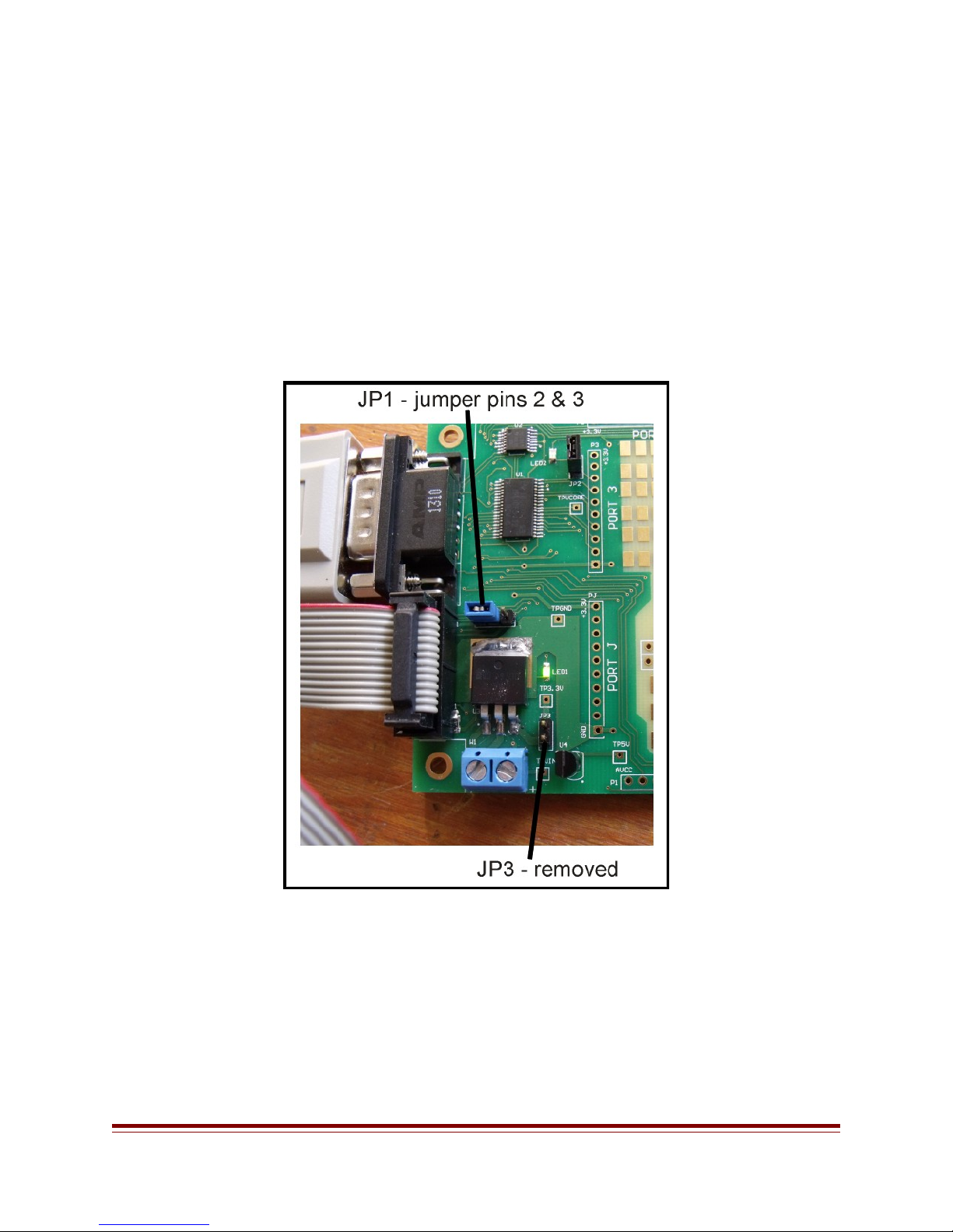
Power Supply
The F5132EX board can be powered in from either the MSP430-FET debugger or through the on
board 3.3V regulator. When powering from the MSP430-FET debugger remove jumper JP3 and short
pins 2 & 3 on JP1 (see photo below). When powering from the on board regulator, install jumper JP3 and
short pins 1 & 2 on JP1.
The main on board voltage regulator is a 3 amp, 3.3 volt low-dropout linear regulator. There is
also a 100 milliamp, 5 volt auxiliary regulator for powering analog circuits. A screw terminal connector
(W1) is provided for connecting to batteries or an external DC power supply. Maximum input voltage on
W1 is 15 volts.
Using MSP430-FET Power
F5132EX User’s Guide Rev. 1.1 – Apr./2016 Page 4

Using Battery (or DC supply) Power
Minimum input voltages (on W1) for proper regulation:
3.8 volts if using only the 3.3V supply
5.5 volts if using both the 3.3V and 5 volt supplies
F5132EX User’s Guide Rev. 1.1 – Apr./2016 Page 5

The Demo Program
The F5132EX board is factory programmed with a simple demo program. To use the demo: leave
the jumpers in their factory setting, connect the board to a PC serial port using the cable included, start
up a terminal program on the PC (Hyperterm or Tera Term, for example) set the port for 9600 bps, 1 stop,
no parity, HW control off. Connect the F5132EX to a DC power supply or battery using connector W1.
You will see the banner on the PC:
***********************************
* EA Electronics *
* MSP430F5132 Demo Program V1.0 *
***********************************
If you type a line in lower case on the terminal program, the demo program echoes back the line
in upper case after you hit the enter key. So if you type:
now hear this.
Followed by the enter key, the program echoes back :
NOW HEAR THIS.
The program also configures all port pins (except P1.1 & P1.2) as outputs and toggles them twice
a second.
Demo Source Code
#include <msp430.h>
#include <stdio.h>
#include <ctype.h>
void initPortPins(void);
void send_msg( char * buf, int len );
char startup1[] = {"\n***********************************\n\r"};
char startup2[] = {"\n* EA Electronics *\n\r"};
char startup3[] = {"\n* MSP430F5132 Demo Program V1.0 *\n\r"};
char startup4[] = {"\n***********************************\n\r"};
char newline[] = {"\n\r"};
#define END_OF_BUFFER 50
void initPortPins(void);
void send_msg( char * buf, int len );
void serial_echo( void );
/*
* main.c
* Serial port echo and toggle IO pins
*/
int main(void) {
WDTCTL = WDTPW | WDTHOLD; // Stop watchdog timer
unsigned int j;
initPortPins();
// set up Serial port for 9600, 1 stop, no parity
UCA0CTL1 |= UCSWRST; // **Put state machine in reset**
UCA0CTL1 |= UCSSEL_1; // CLK = ACLK
UCA0BR0 = 0x03; // 32kHz/9600
UCA0BR1 = 0x00; //
UCA0MCTL = UCBRS_3+UCBRF_0; // Modulation UCBRSx=3, UCBRFx=0
UCA0CTL1 &= ~UCSWRST; // release USCI for operation
F5132EX User’s Guide Rev. 1.1 – Apr./2016 Page 6

// print start-up banner
send_msg( newline, sizeof(newline) );
send_msg( startup1, sizeof(startup1) );
send_msg( startup2, sizeof(startup2) );
send_msg( startup3, sizeof(startup3) );
send_msg( startup4, sizeof(startup4) );
for(;;)
{
for( j=0; j<15000; j++)
{
serial_echo();
}
P3OUT = (0xAA);
P2OUT = (0xAA);
P1OUT = (0xAA);
PJOUT = (0xAA);
{
}
return 0;
}
// echo routine
unsigned int b = 0; // buffer index
char inbuf[END_OF_BUFFER];
void serial_echo( void )
{
// check for a character on the input
if(UCA0IFG&UCRXIFG)
{
}
}
for( j=0; j<15000; j++)
serial_echo();
}
P3OUT = (0x55);
P2OUT = (0x55);
P1OUT = (0x55);
PJOUT = (0x55);
// save it in the buffer
inbuf[b] = toupper(UCA0RXBUF);
b++;
// check for end of line or buffer full
if( (inbuf[b] == '\r') || (b == END_OF_BUFFER) )
{
// echo the message
send_msg( inbuf, b-1 );
send_msg( newline, sizeof(newline) );
b = 0;
}
F5132EX User’s Guide Rev. 1.1 – Apr./2016 Page 7

void send_msg( char * buf, int len )
{
}
void initPortPins(void)
{
int i;
for( i=0; i<len;)
{
if(UCA0IFG&UCTXIFG) // USCI_A0 TX buffer ready?
{
UCA0TXBUF = ( buf[i] ); // TX -> RXed character
i++;
}
else
{
continue;
}
}
P1DIR |= BIT1; // Set P1.1 as TX output
P1SEL |= BIT1 + BIT2; // Select P1.1 & P1.2 to UART function
P2DIR = 0xFF; // all pins as outputs
P3DIR = 0xFF; // all pins as outputs
}
PJDIR = 0xFF; // all pins as outputs
You can download the entire Code Composer project for the demo program, go to:
www.eaelec.com\ea_eval\eval.htm
F5132EX User’s Guide Rev. 1.1 – Apr./2016 Page 8

The Serial Port
The serial port utilizes only 3 pins on the DB9M connector (TX, RX and GND). A null modem
serial cable is included for connection to a PC serial port .
Cable Drawing
F5132EX User’s Guide Rev. 1.1 – Apr./2016 Page 9

Bill of Materials
F5132EX User’s Guide Rev. 1.1 – Apr./2016 Page 10
 Loading...