

Page 1

ADC EV10AS150A Evaluation Board
User Guide
Page 2

2 ADC EV10AS150A User Guide
0977B–BDC–09/09
Page 3

Table of Contents
Section 1
Introduction ........................................................................................... 1-1
1.1 Scope1-1
1.2 Description ................................................................................................1-1
Section 2
Hardware Description ........................................................................... 2-1
2.1 Board Structure .........................................................................................2-1
2.2 Analog Inputs/Clock Input .........................................................................2-2
2.3 Digital Output ............................................................................................2-3
2.4 Reset Lines ...............................................................................................2-5
Section 3
Operating Characteristics ..................................................................... 3-1
3.1 Introduction ...............................................................................................3-1
3.2 Operating Procedure.................................................................................3-1
3.3 Electrical Characteristics...........................................................................3-2
3.4 Digital Output Coding ................................................................................3-4
Section 4
Software Tools...................................................................................... 4-1
4.1 Overview ...................................................................................................4-1
4.2 Configuration.............................................................................................4-1
4.3 Getting Started ..........................................................................................4-1
4.4 Operating Modes ......................................................................................4-7
Section 5
Application Information .........................................................................5-1
5.1 Introduction ...............................................................................................5-1
5.2 Analog Inputs ............................................................................................5-1
5.3 Clock Inputs ..............................................................................................5-1
5.4 Digital Outputs ..........................................................................................5-1
5.5 ADC Functions ..........................................................................................5-2
5.6 DMUX Functions .......................................................................................5-2
5.7 Diode for Die Junction Temperature Monitoring .......................................5-4
5.8 Test Bench Description .............................................................................5-6
Section 6
Package Information............................................................................. 6-1
6.1 Thermal Characteristics ............................................................................6-1
EV10AS150A-EB User Guide 1
0977B–BDC–10/09
Page 4

Section 7
Ordering Information............................................................................. 7-1
Section 8
Appendix............................................................................................... 8-1
8.1 EV10AS150A-EB Electrical Schematics ...................................................8-1
8.2 EV10AS150A-EB Board Layers................................................................8-9
2 EV10AS150A-EB User Guide
0977B–BDC–10/09
Page 5

Section 1
Introduction
1.1 Scope The ADC EV10AS150A-EB Evaluation Kit is designed to facilitate the evaluation and
characterization of the different versions of EV10AS150A ADC with 1:2/4 DMUX up to
its 5 GHz full power input bandwidth.
The ADC EV10AS150A-EB Evaluation Kit includes:
The EV10AS150A with 1:2/4 DMUX Evaluation board including one version of the
EV10AS150A ADC device soldered on the board
Six SMA caps for CLK, CLKN, VIN, VINN, DRR and ASYNCRST signals
Six jumpers DMUX function settings (RS, BIST, DRTYPE, SLEEP, STAGG),
CLKTYPE jumper is not used
3-wire serial link to control ADC functionality
The user guide uses the EV10AS150A Evaluation Kit as an evaluation and demonstra-
tion platform and provides guidelines for its proper use.
1.2 Description The ADC EV10AS150A Evaluation board is very straightforward as it only implements
the EV10AS150A ADC/DMUX device, SMA connectors for the sampling clock, analog
inputs and reset inputs accesses and HE14 double row 2.54 mm pitch connectors compatible with high speed acquisition system probes.
To achieve optimal performance, the ADC EV10AS150A-EB Evaluation board was
designed in a 8-metal-layer board with RO4003 200 µm and FR4 HTG epoxy dielectric
materials. The board implements the following devices:
The ADC EV10AS150A with 1:2/4 DMUX Evaluation board with one version of the
EV10AS150A ADC soldered on the board
Six SMA caps for CLK, CLKN, VIN, VINN, DRR and ASYNCRST signals
Six jumpers DMUX function settings (RS, BIST, DRTYPE, SLEEP, STAGG),
CLKTYPE jumper is not used
3-wire serial link to control ADC functionality via RS232
2.54 mm pitch connectors for the digital outputs, compatible with high speed
acquisition system probes
Banana jacks for the power supply accesses and the die junction temperature
monitoring functions (2 mm)
Potentiometers for the DMUX functions
EV10AS150A-EB User Guide 1-1
e2v semiconductors SAS 2009
0977B–BDC–10/09
Page 6
Introduction
The board is composed of eight metal layers for signal traces, ground and power supply
layers, and seven dielectric layers featuring low insertion loss and enhanced thermal
characteristics for operation in the high frequency domain.
The board dimensions are 220 mm x 240 mm.
The board comes fully assembled and tested, with one version of the EV10AS150A
ADC installed.
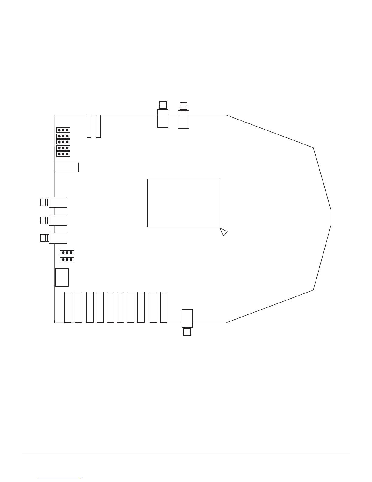
Figure 1-1. ADC EV10AS150A-EB Evaluation Board Simplified Schematic
CLKNCLK
Diode
DMUX functions
CLKDACTRL
DRR
ADC
EV10AS150A
Port D
Port C
VINN
VIN
G
N
D
RS232
3
V
3
DMUX functions
V
C
C
A
3
G
N
D
G
N
3
V
D
3
PIN 1
V
C
C
A
5
5
v
2
V
C
C
D
G
3
N
v
D
3
V
+
D
G
2
N
V
D
ASYNCRST
5
Port A
As shown in Figure 1-1, different power supplies are required:
V
V
V
V
= 5.0V analog positive power supply
CCA5
= 3.3V analog positive power supply
CCA3
= 3.3V digital positive power supply
CCD
= 2.5V digital output power supply
PLUSD
3.3V power supply for the board functions
DR
Port B
1-2 EV10AS150A-EB User Guide
0977B–BDC–10/09
e2v semiconductors SAS 2009
Page 7

2.1 Board Structure
In order to achieve optimum full speed operation of the ADC EV10AS150A with 1:2/4
DMUX, a multilayer board structure was retained for the evaluation board. Eight copper
layers are used, respectively dedicated to the signal traces, ground planes, power supply planes and DC signals traces.
The board is made in RO4003 200 µm and FR4 HTG epoxy dielectric materials. Table
2-1 gives a detailed description of the board's structure.
Table 2-1. Board Layer Thickness Profile
Layer Characteristics
Copper thickness = 40 µm
Layer 1
Copper layer
AC signals traces = 50Ω microstrip lines
DC signals traces (DMUX functionality etc.)
Section 2
Hardware Description
Layer thickness = 200 µm
Dielectric constant = 3.4 at 10 GHz
Layer 2
RO4003 dielectric layer (Hydrocarbon/wovenglass)
Layer 3
Copper layer
Layer 4
FR4 HTG/dielectric layer Layer thickness = 170 µm
Layer 5
Copper layer
Layer 6
FR4 HTG/dielectric layer Layer thickness = 200 µm
Layer 7
Copper layer
Layer 8
FR4 HTG/dielectric layer Layer thickness = 170 µm
EV10AS150A-EB User Guide 2-1
–0.044 dB/inch insertion loss at 2.5 GHz
–0.318 dB/inch insertion loss at 18 GHz
Copper thickness = 35 µm
Upper ground plane = reference plane 50Ω microstrip return
Copper thickness = 35 µm
Power planes = V
Copper thickness = 35 µm
Power planes = V
CCA5
and 3.3V
CCD
e2v semiconductors SAS 2009
0977B–BDC–10/09
Page 8

Hardware Description
Table 2-1. Board Layer Thickness Profile (Continued)
Layer 9
Copper layer
Layer 10
FR4 HTG/dielectric layer Layer thickness = 200 µm
Layer 11
Copper layer
Layer 12
FR4 HTG/dielectric layer Layer thickness = 170 µm
Layer 13
Copper layer
Layer 14
FR4 HTG/dielectric layer Layer thickness = 200 µm
Layer 15
Copper layer
Copper thickness = 35 µm
Power planes = V
Copper thickness = 35 µm
Power planes = V
Copper thickness = 35 µm
Ground plane = reference plane (identical to layer 3)
Copper thickness = 40 µm
DC signals traces and Serial Interface (AVR) signals
Ground plane
CCA3
PLUSD
The board is 1.6 mm thick.
The clock, analog input, reset and digital data output signals occupy the top metal layer
while the ADC and DMUX functions are located both on the top.
The ground planes occupy layer 3, 13 and 15 (partly).
2.2 Analog
Inputs/Clock
Input
Layer 5, 7, 9 and 11 are dedicated to the power supplies.
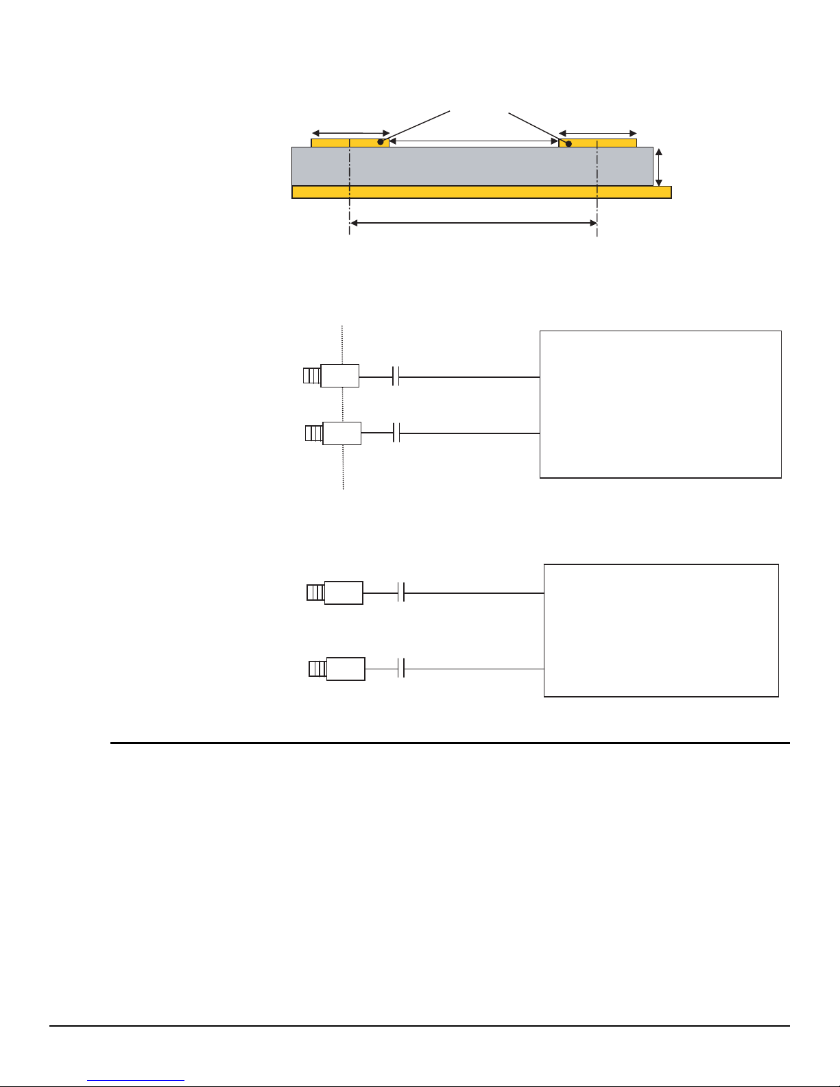
The differential active inputs (Clock, Analog) are provided by SMA connectors.
Reference: VITELEC 142-0701-8511
Special care was taken for the routing of the analog input and clock input signals for
optimum performance in the high frequency domain:
50Ω lines matched to ±0.1 mm (in length) between V
and V
IN
and between CLK
INN
and CLKN
50 mm max line length
1.27 mm pitch between the differential traces
400 µm line width
40 µm thickness
850 µm diameter hole in the ground layer below the V
, V
IN
, CLK and CLKN ball
INN
footprints
2-2 EV10AS150A-EB User Guide
0977B–BDC–10/09
e2v semiconductors SAS 2009
Page 9
Hardware Description
Figure 2-1. Figure 2-1.Board Layout for the Differential Analog and Clock Inputs
400 µm
e= 40µm
m
870 µ
400 µm
RO4003
Ground plane
µ1270 m
Figure 2-2. Differential Analog Inputs Implementation
100 pF
VIN
VINN
100 pF
VIN (H27)
VINN
Figure 2-3. Differential Clock Inputs Implementation
(J27)
200 µ m
EV10AS150A
100 pF
CLK
CLKN
100 pF
CLK (W23)
EV10AS150A
CLKN (RW24)
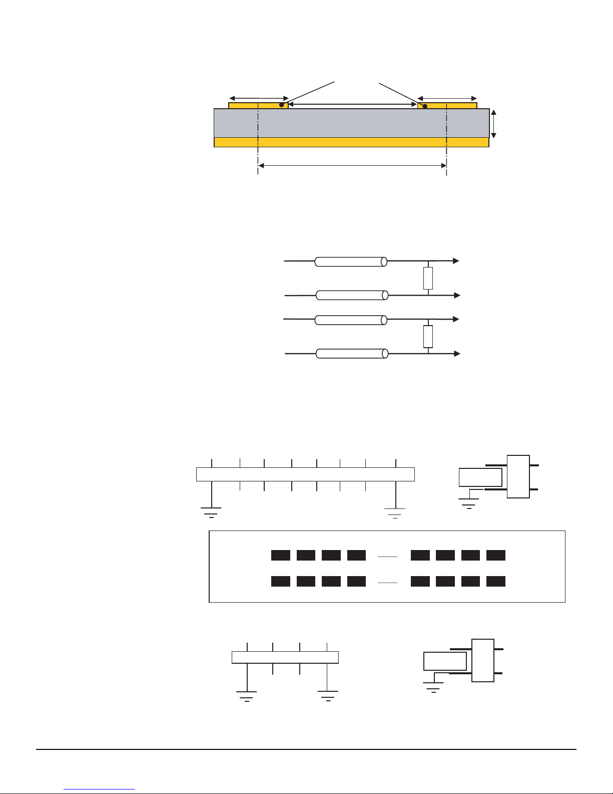
2.3 Digital Output The digital output lines were designed with the following recommendations:
50Ω lines matched to ±0.5 mm (in length) between signal of the same differential pair
80 mm max line length
±1 mm line length difference between signals of two ports
±1.5 mm max line length difference between all signals
770 µm pitch between the differential traces
370 µm line width
40 µm thickness
EV10AS150A-EB User Guide 2-3
e2v semiconductors SAS 2009
0977B–BDC–10/09
Page 10
Hardware Description
Figure 2-4. Board Layout for the Differential Digital Outputs
3 7 0 µ m
e= 40µm
400 µm
370 µm
RO4003
Ground Plane
m
770 µ
200 µm
The digital outputs are compatible with LVDS standard. They are on-board 100Ω differentially terminated as described in Figure 2-5.
Figure 2-5. Differential digital Outputs Implementation
Line
50Ω
50Ω
50Ω
50Ω
Line
Line
Line
100Ω
100Ω
Di
DiN
DRN
DR
HE14 Double row 2.54 mm pitch connectors are used for the digital output data. The
upper row is connected to the signal while the lower row is connected to Ground, as
illustrated in Figure 2-6.
Figure 2-6. Differential Digital Outputs 2.54 mm Pitch Connector (Example Port A)
Signal
Ground
A0N A0 AORN
…
GND A0N A0
GND GND GND GND GND GND GND GND
AOR
A
/DR
/DRA
N
A1N AORN AOR GND B0
Figure 2-7. Differential Digital Clock Outputs 2.54 Mm Pitch Connector
l
Signa
DR
DR
N
Ground
2-4 EV10AS150A-EB User Guide
0977B–BDC–10/09
e2v semiconductors SAS 2009
Page 11
Hardware Description
µ
2.4 Reset Lines
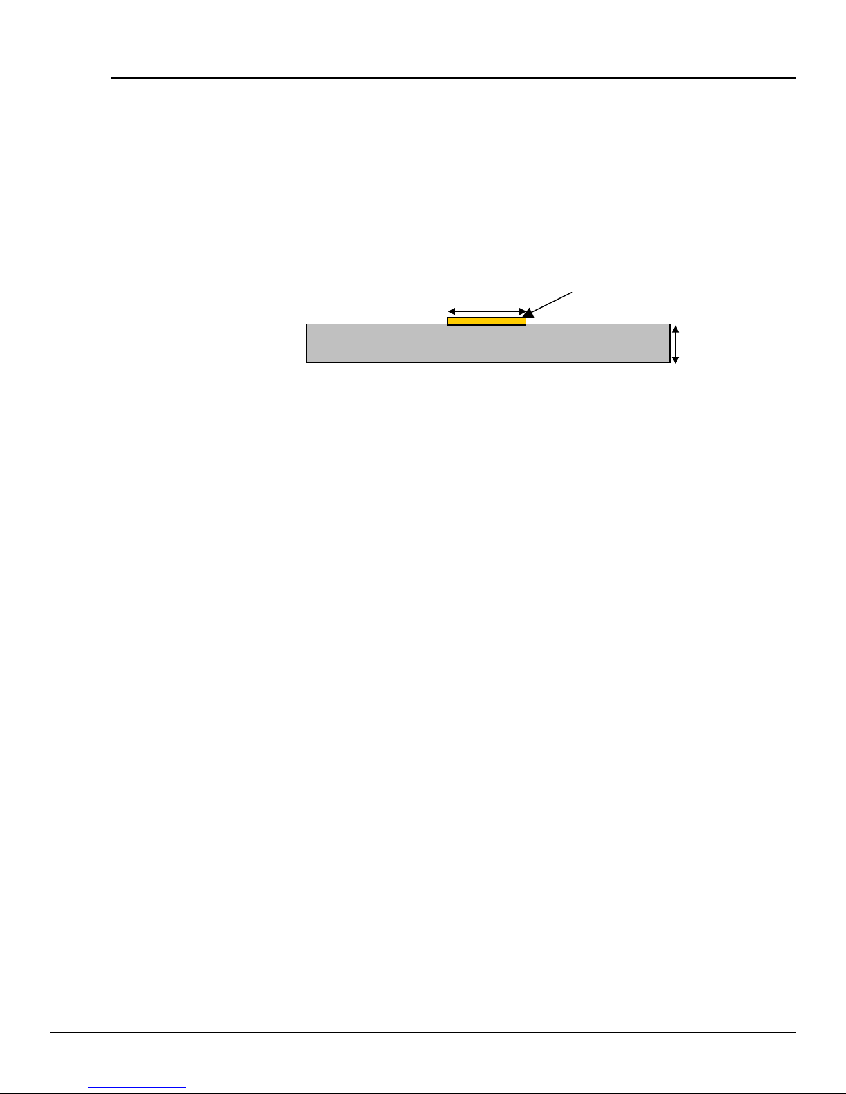
The reset line (DRR and ASYNCRST) were designed with the following recommendations:
50Ω lines
80 mm max line length
430 µm line width
40 µm thickness
Figure 2-8. Board Layout for the Single Reset Lines
430 µm
RO4003
e=40
m
200 µm
EV10AS150A-EB User Guide 2-5
e2v semiconductors SAS 2009
0977B–BDC–10/09
Page 12

Hardware Description
2-6 EV10AS150A-EB User Guide
0977B–BDC–10/09
e2v semiconductors SAS 2009
Page 13

Section 3
Operating Characteristics
3.1 Introduction This section describes a typical configuration for operating the evaluation board of the
ADC EV10AS150A with 1:2/4 DMUX.
The analog input signal can be entered either in differential or single ended. Refer to the
datasheet for the impact of driving analog input in single or in differential. The clock input
signal must be differentially driven.
ADC EV10AS150 clock inputs should be fed with balanced signals (use a balun or
hybrid junction to convert a single signal to a differential signal).
3.2 Operating
Procedure
1. Connect the power supplies and ground accesses through the dedicated banana
jacks.
V
= 5.0V, V
CCA5
V
= 3.3V, V
CCA3
short-cable.
2. Connect the clock input signals. Use a low-phase noise high frequency
generator.
The clock input level is typically 1dBm (on 100Ω differential input). The clock frequency
can range from 500 MHz up to maximum speed.
3. Connect the analog input signal. Use a low-phase noise high frequency
generator.
The analog input full scale is 500 mV peak-to-peak (±250 mV on each single ended
input) around 0V (AC coupling). It is recommended to use the ADC with an input signal
of –1 dBFS max (to avoid saturation of the ADC).
The analog input frequency can range from DC up to 5 GHz. At 5 GHz, the ADC attenuates the input signal by 3 dB.
4. Connect the high-speed acquisition system probes to the output connectors.
The digital data are differentially terminated on-board (100Ω) however, they can be
probed either in differential or in single-ended mode.
5. Connect the DMUX function jumpers:
All instrumentation and connectors are now connected.
6. Switch on the power supplies (No specific power supplies sequencing required
during power on/off).
7. Turn on the RF clock generator.
8. Turn on the RF signal generator.
= 3.3V, V
CCA3
= 3.3V and 3.3V have separated planes but can be reunited via a
CCD
= 3.3V, V
CCD
PLUSD
= 2.5V,
EV10AS150A-EB User Guide 3-1
0977B–BDC–10/09
e2v semiconductors SAS 2009
Page 14

Operating Characteristics
9. Perform an asynchronous Reset (DRR active) on the device and maintain this
Reset active.
10. Perform an asynchronous Reset ((push button) ASYNCRST active) on the
board.
11. Then, ASYNCRST inactive on the board.
12. DRR inactive on the device.
13. Started 3 Wire Serial interface (refer to Section 4)
14. Reset button allows to configure ADC (Mode 0)
3.3 Electrical
Characteristics
Table 3-1. Absolute Maximum Ratings
Parameter Symbol Value Unit
Analog 5.0V Power Supply voltage V
Analog 3.3V Power Supply voltage V
Digital 3.3V Power Supply Voltage V
Output 2.5V Power Supply voltage V
Minimum Analog input peak voltage
CCA5
CCA3
CCD
PLUSD
V
IN
or V
INN
(with differential input)
Maximum Analog input peak voltage
or V
V
IN
INN
(with differential input)
Maximum difference between V
V
INN
IN
and
|V
- V
|2.0
IN
INN
(with differential input)
Minimum Analog input peak voltage
(with single ended input)
VIN with VINN = 50Ω to GND
or
VINN with VIN = 50Ω to GND
Maximum Analog input peak voltage
(with single ended input)
Maximum amplitude on V
IN
or V
INN
V
or
V
|V
with V
IN
with V
INN
IN|
or |V
= 50Ω to GND
INN
= 5 Ω to GND
IN
| (2 Vpp = +10 dBm in 50Ω)V
INN
(with single ended input)
Minimum Clock input peak voltage
or V
V
CLK
CLKN
(with differential clock)
Maximum Clock input peak voltage
or V
V
CLK
CLKN
(with differential clock)
Maximum difference between V
and V
CLKN
CLK
CLK - VCLKN
|1.5
|V
(with differential clock)
3WSI input voltage SDATA, SLDN, SCLK, RESET –0.3 to
ADC Reset Voltage DRR –0.3 to V
DMUX function input voltage RS, DRTYPE, SLEEP, STAGG, BIST –0.3 to V
DMUX Asynchronous Reset ASYNCRST –0.3 to V
GND to 6.0 V
GND to 3.6 V
GND to 3.6 V
GND to 3.0 V
2.0 V
4.0 V
(4 Vpp = +13 dBm in 100 Ω)
2.0 V
4.0 V
1.5 V
4.0 V
(3 Vpp)
+ 0.3 V
VCCA3
+ 0.3 V
CCA3
+ 0.3 V
CCD
+ 0.3 V
CCD
V
V
3-2 EV10AS150A-EB User Guide
0977B–BDC–10/09
e2v semiconductors SAS 2009
Page 15

Operating Characteristics
Table 3-1. Absolute Maximum Ratings (Continued)
DMUX Control Voltage CLKDACTRL –0.3 to V
Maximum input voltage on DIODE DIODE ADC 700 mV
Maximum input current on DIODE DIODE ADC 1 mA
Max Junction Temperature T
J
135 °C
Storage temperature Tstg –55 to 150 °C
ESD protection (HBM) ≥500 on ADC inputs
500 on DMUX outputs
Note: Absolute maximum ratings are limiting values (referenced to GND = 0V), to be applied individually, while other parameters are
within specified operating conditions. Long exposure to maximum rating may affect device reliability.
All integrated circuits should be handled with appropriate care to avoid damages due to ESD. Damage caused by inappropriate
handling or storage could range from performance degradation to complete failure, including reliability degradation.
+ 0.3 V
CCD
V
Table 3-2. Electrical Characteristics for Supplies
Test
Parameter
POWER REQUIREMENTS
Power Supply voltages
Analog 5.0V
Analog 3.3V
Digital 3.3V
Output 2.5V
Power Supply current in 1:2 DMUX
Analog V
Analog V
Digital V
Output V
CCA5
CCA3
CCD
PLUSD
= 5.0V
= 3.3V
= 3.3V
= 2.5V
Power Supply current in 1:4 DMUX
Analog V
Analog V
Digital V
Output V
CCA5
CCA3
CCD
PLUSD
= 5.0V
= 3.3V
= 3.3V
= 2.5V
Power Supply current in NAP and SLEEP mode
Analog V
Analog V
Digital V
Output V
CCA5
CCA3
CCD
PLUSD
= 5.0V
= 3.3V
= 3.3V
= 2.5V
Power dissipation
- 1:2 DMUX
- 1:4 DMUX
- NAP & SLEEP mode (1:4 or 1:2)
Level
1
1
1
1
1 P
Symbol Min Typ Max Unit
V
CCA5
V
CCA3
V
CCD
V
PLUSD
I
VCCA5
I
VCCA3
I
VCCD
I
VPLUSD
I
VCCA5
I
VCCA3
I
VCCD
I
VPLUSD
I
VCCA5
I
VCCA3
I
VCCD
I
VPLUSD
D
4.85
3.15
3.15
2.4
5.0
3.3
3.3
2.5
160
775
400
420
160
775
450
450
140
590
140
410
6.2
6.4
4.4
5.15
3.45
3.45
2.6
200
960
500
610
200
960
580
650
190
870
180
560
7.6
8.0
6.0
V
V
V
V
mA
mA
mA
mA
mA
mA
mA
mA
mA
mA
mA
mA
W
W
W
EV10AS150A-EB User Guide 3-3
0977B–BDC–10/09
e2v semiconductors SAS 2009
Page 16

Operating Characteristics
3.4 Digital Output
Coding
Table 3-3. Digital Output Coding
Differential
Analog Input Voltage Level Digital Output
Natural Binary
MSB……….LSB OR
> 250.25 mV >Top end of full scale + ½ LSB 1 1 1 1 1 1 1 1 1 1 1 0 1 1 1 1 1 1 1 1 1 1 1 0 0 0 0 0 0 0 0 0 1
250.25 mV
249.75 mV
125.25 mV
124.75 mV
0.25 mV
–0.25 mV
–124.75 mV
–124.25 mV
–249.75 mV
–250.25 mV
Top end of full scale + ½ LSB
Top end of full scale - ½ LSB
3
/4 full scale + ½ LSB
3
/4 full scale - ½ LSB
Mid scale + ½ LSB
Mid scale - ½ LSB
1
/4 full scale + ½ LSB
1
/4 full scale - ½ LSB
Bottom end of full scale + ½ LSB
Bottom end of full scale - ½ LSB
1 1 1 1 1 1 1 1 1 1 0
1 1 1 1 1 1 1 1 1 0 0
1 1 0 0 0 0 0 0 0 0 0
1 0 1 1 1 1 1 1 1 1 0
1 0 0 0 0 0 0 0 0 0 0
0 1 1 1 1 1 1 1 1 1 0
0 1 0 0 0 0 0 0 0 0 0
0 0 1 1 1 1 1 1 1 1 0
0 0 0 0 0 0 0 0 0 1 0
0 0 0 0 0 0 0 0 0 0 0
<–250.25 mV < Bottom end of full scale - ½ LSB 0 0 0 0 0 0 0 0 0 0 1 1 0 0 0 0 0 0 0 0 0 1 0 0 0 0 0 0 0 0 0 0 1
(1)
Binary 2’s Complement
MSB……....LSB OR
0 1 1 1 1 1 1 1 1 1 0
0 1 1 1 1 1 1 1 1 0 0
0 1 0 0 0 0 0 0 0 0 0
0 0 1 1 1 1 1 1 1 1 0
0 0 0 0 0 0 0 0 0 0 0
1 1 1 1 1 1 1 1 1 1 0
1 1 0 0 0 0 0 0 0 0 0
1 0 1 1 1 1 1 1 1 1 0
1 0 0 0 0 0 0 0 0 1 0
1 0 0 0 0 0 0 0 0 0 0
(1)
Gray Coding
MSB……..LSB OR
1 0 0 0 0 0 0 0 0 0 0
1 0 0 0 0 0 0 0 0 1 0
1 0 1 0 0 0 0 0 0 0 0
1 1 1 0 0 0 0 0 0 0 0
1 1 0 0 0 0 0 0 0 0 0
0 1 0 0 0 0 0 0 0 0 0
0 1 1 0 0 0 0 0 0 0 0
0 0 1 0 0 0 0 0 0 0 0
0 0 0 0 0 0 0 0 0 1 0
0 0 0 0 0 0 0 0 0 0 0
(1)
MSB bit 9 and LSB bit 0.
Note: 1. Refer to chap. 4.4.4 and 4.4.5 for selection between natural binary, binary 2's complement or Gray coding.
3-4 EV10AS150A-EB User Guide
0977B–BDC–10/09
e2v semiconductors SAS 2009
Page 17

Section 4
Software Tools
4.1 Overview The ADC EV10AS150A evaluation user interface software is a C++ compiled graphical
interface.
No license is required to run on a W98, NT, W2000 and XP PC.
The software uses intuitive push buttons and popup menus to write data from the
hardware.
4.2 Configuration Advised configuration for Win2000:
– PC Pentium >100 MHz
– Memory 24Mo
– For other versions of Windows OS, use the recommended configuration from
Microsoft
– Two COM ports are necessary to use two boards simultaneously
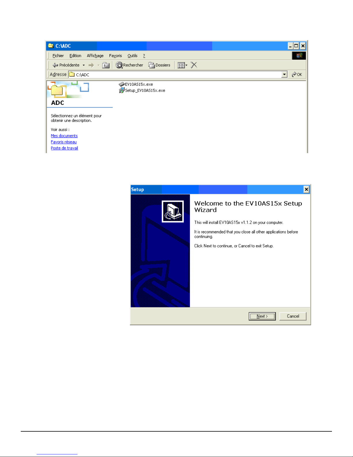
4.3 Getting Started Install the ADC EV10AS15x application on your computer by launching the EV10AS15x
exe installer.
EV10AS150A-EB User Guide 4-1
e2v semiconductors SAS 2009
0977B–BDC–10/09
Page 18
Software Tools
Figure 4-1. Install Window
Start the Setup_EV10AS15x (v1.1.2)
Figure 4-2. EV10AS150A Application Set up Wizard Window
4-2 EV10AS150A-EB User Guide
0977B–BDC–10/09
e2v semiconductors SAS 2009
Page 19
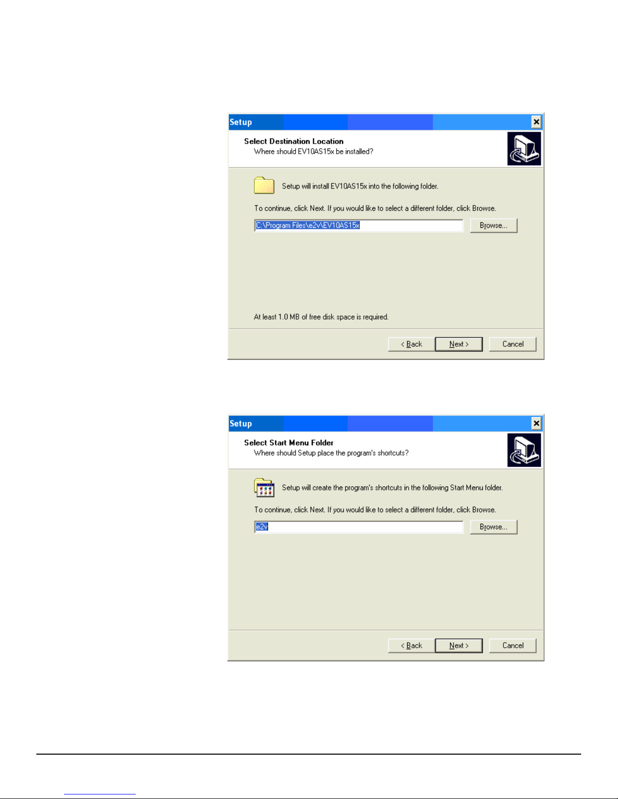
Next step: Select Destination Directory.
Figure 4-3. EV10AS150A select Destination Directory Window
Software Tools
Next step: Start Menu Folder.
Figure 4-4. EV10AS150A select Start Menu Window
EV10AS150A-EB User Guide 4-3
e2v semiconductors SAS 2009
0977B–BDC–10/09
Page 20
Software Tools
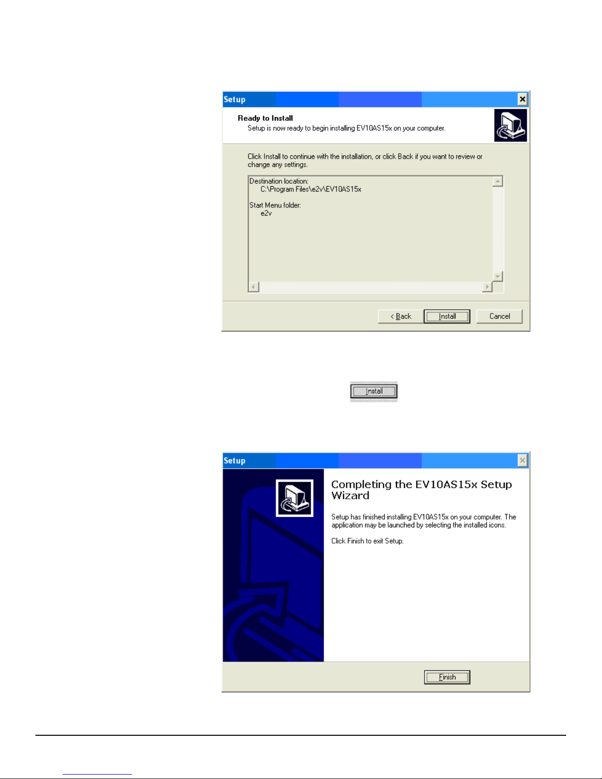
Next step: verification of the install configuration.
Figure 4-5. EV10AS150A Ready to Install Window
If you agree with the install configuration press Install.
Figure 4-6. EV10AS150A Application Setup Install Push Button
The software is completing installation.
Figure 4-7. EV10AS150A Completing Setup Wizard Window
4-4 EV10AS150A-EB User Guide
0977B–BDC–10/09
e2v semiconductors SAS 2009
Page 21
Software Tools
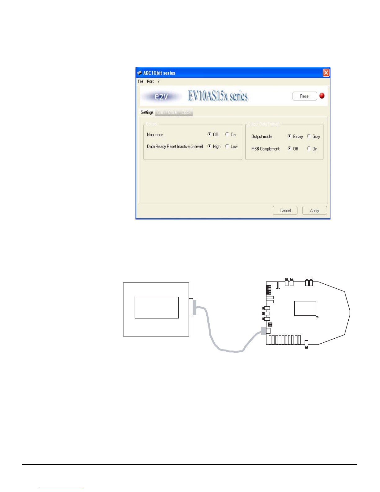
Now you can launch the ADC10Bit series software from its icon; the following screen will
be displayed:
Figure 4-8. ADC EV10AS150A User Interface Window
Figure 4-9. ADC10-bit User Interface Hardware Implementation
Evaluation
Board
ADC EV10AS150A
PC
Software
Serial port
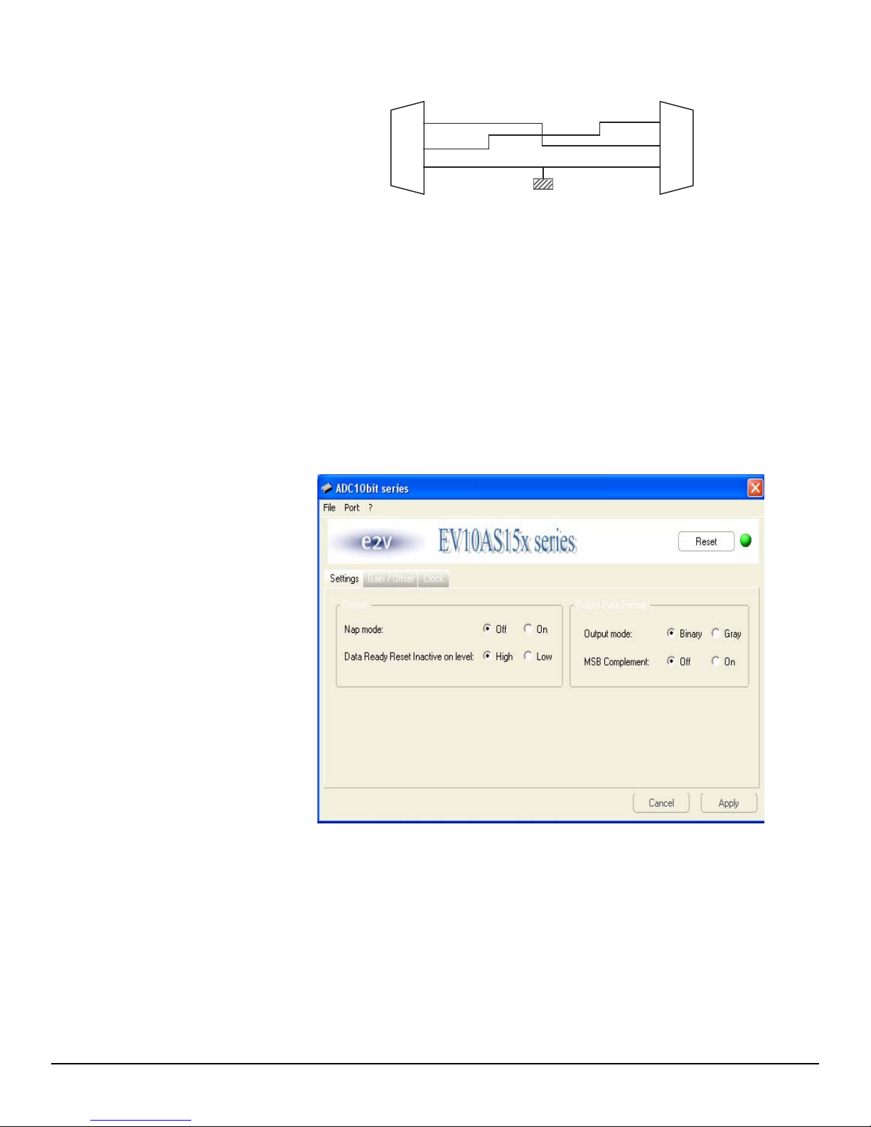
Use a RS 232 port to send data to ADC.
Connect the crossed DB9 9 (F/F) cable between your PC and your evaluation board.
EV10AS150A-EB User Guide 4-5
e2v semiconductors SAS 2009
0977B–BDC–10/09
Page 22
Software Tools
Figure 4-10. Crossed RS232 Cable
DB 9
Female
2
3
5
2
DB 9
Female
3
5
Serial Port Configuration:
Bit rate: 19200
Data coding: 8 bit
1 start bit, 1 Stop bit
No parity check
4.3.1 Installation Software At startup, the application automatically checks all RS 232 ports available on the computer and tries to find the evaluation board on them.
Figure 4-11. ADC EV10AS150A User Interface
The Port menu shows all available ports on your computer. The port currently used has
a check mark on its left. By clicking another port item, the application will try to connect
to an evaluation board via the selected port. If a board is successfully detected on the
new port, the LED is green (or orange depending on the serial interface switch) and the
new port gets the check mark. If the application is not able to find a board on this port,
an error message is displayed and the LED turns to red.
4-6 EV10AS150A-EB User Guide
0977B–BDC–10/09
e2v semiconductors SAS 2009
Page 23
4.3.2 Troubleshooting
Software Tools
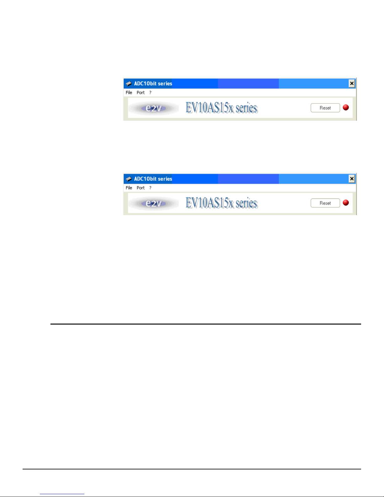
If the ADC EV10AS150A evaluation board is not connected or not powered, a red LED
appears on the right of the Reset button and the application is grayed
Figure 4-12. ADC EV10AS150A User Interface
Check the connection to the PC and restart the application.
If the serial interface is not active the LED appears in orange and the application is
grayed too.
Figure 4-13. ADC EV10AS150A User Interface
Turn ON the switch on the demo board, the application should become available and
the LED turns to green.
Troubleshooting:
– Check your rights to write in the directory
– Check for the available disk space
– Check that at least one RS232 serial port is free and properly configured.
– Check that the DB9 connector is properly inserted
– Check that all supplies are ON
– Check that the serial mode is active (green LED ON)
4.4 Operating Modes
4.4.1 Overview The software provides a graphical user interface to configure the ADC.
Push buttons, popup menus and capture windows allows playing with:
Control Mode,
Switch analog and Switch clock
Standby
Gain
Offset
DDA
EV10AS150A-EB User Guide 4-7
e2v semiconductors SAS 2009
0977B–BDC–10/09
Page 24
Software Tools
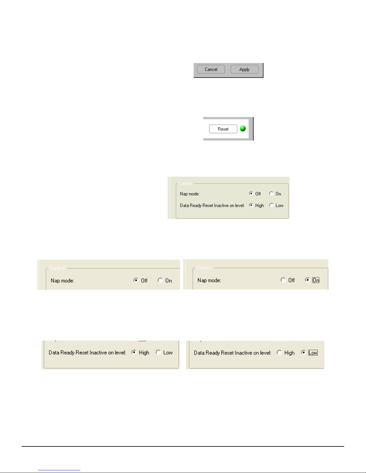
Always click on Apply to validate any command
Each setting must be validated in its own tab.
Clicking on Cancel will restore last settings sent with Apply button.
Reset button allows to configure ADC (Mode 0)
4.4.2 Control Mode The control mode allows controlling the NAP mode and Data Ready Reset Inactive
mode.
4.4.2.1 NAP Mode NAP mode configurable Off or On
4.4.2.2 Data Ready Reset
Inactive on Level
Data Ready Reset is inactive on High level or on Low level
4-8 EV10AS150A-EB User Guide
0977B–BDC–10/09
e2v semiconductors SAS 2009
Page 25
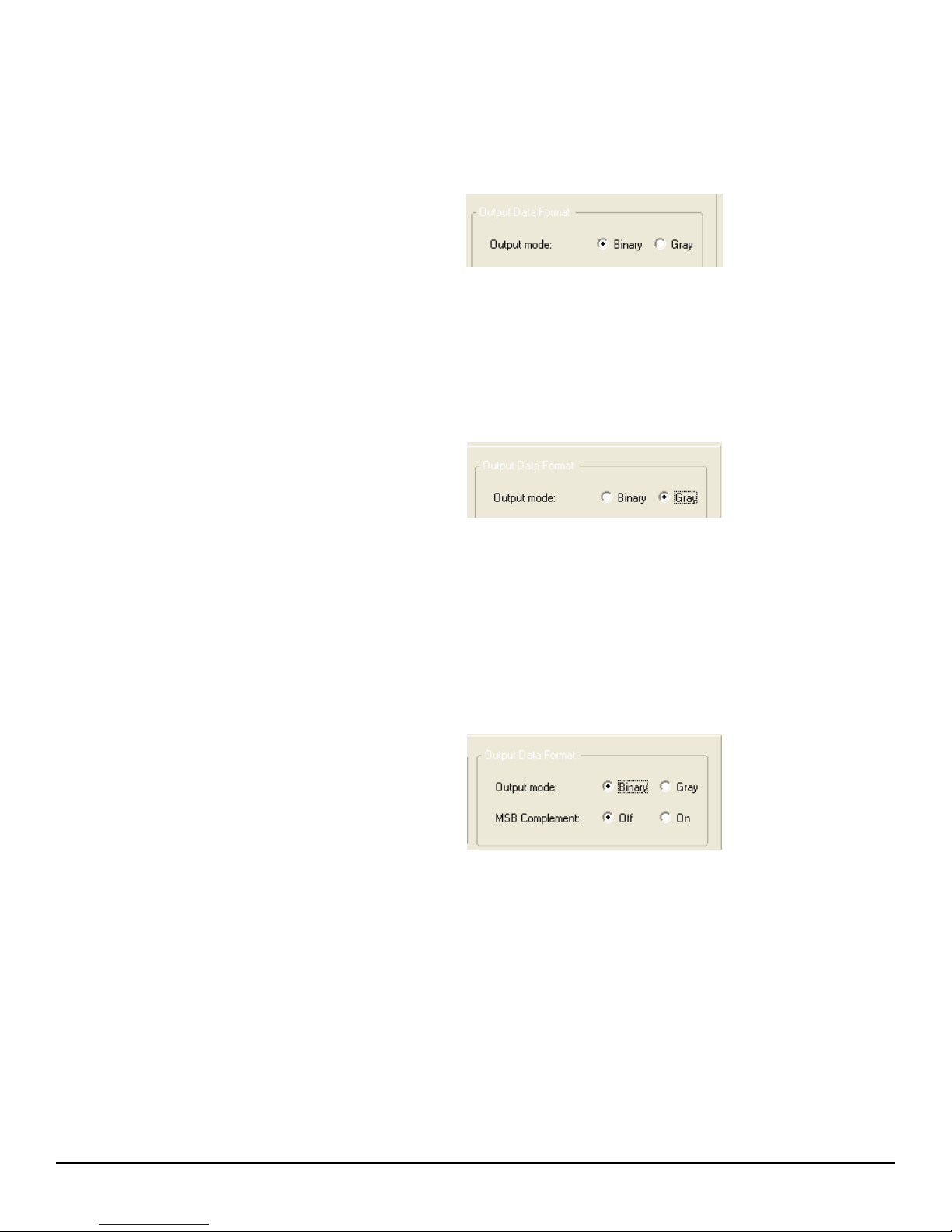
4.4.3 ADC Output Data
Format (BinaryGray)
Software Tools
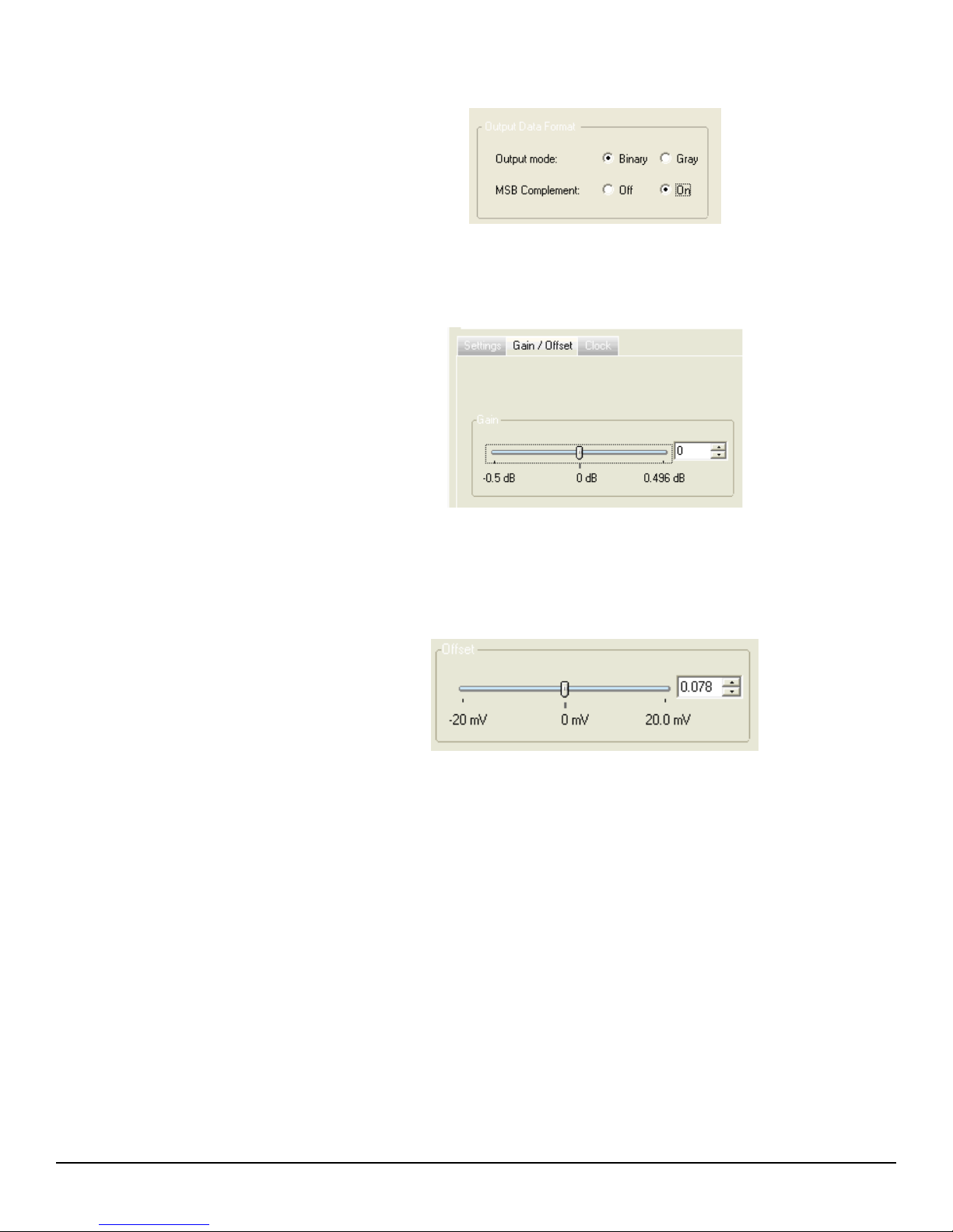
ADC Output Data Format: Binary
ADC Output Data Format: Gray
Note: In this mode, MSB complement is not available.
4.4.4 ADC Output Data
Format (MSB
Complement)
ADC Output Data Format: MSB complement Off
ADC Output Data Format: MSB complement On
Note: Mode MSB complement is available if ADC output data format is binary
EV10AS150A-EB User Guide 4-9
e2v semiconductors SAS 2009
0977B–BDC–10/09
Page 26
Software Tools
4.4.5 ADC Gain Adjust ADC Gain adjustment is from –0.5 to 0.5 dB.
4.4.6 ADC Offset Adjust
ADC Offset adjustment is from –20 mV to 20 mV.
4-10 EV10AS150A-EB User Guide
0977B–BDC–10/09
e2v semiconductors SAS 2009
Page 27
Software Tools
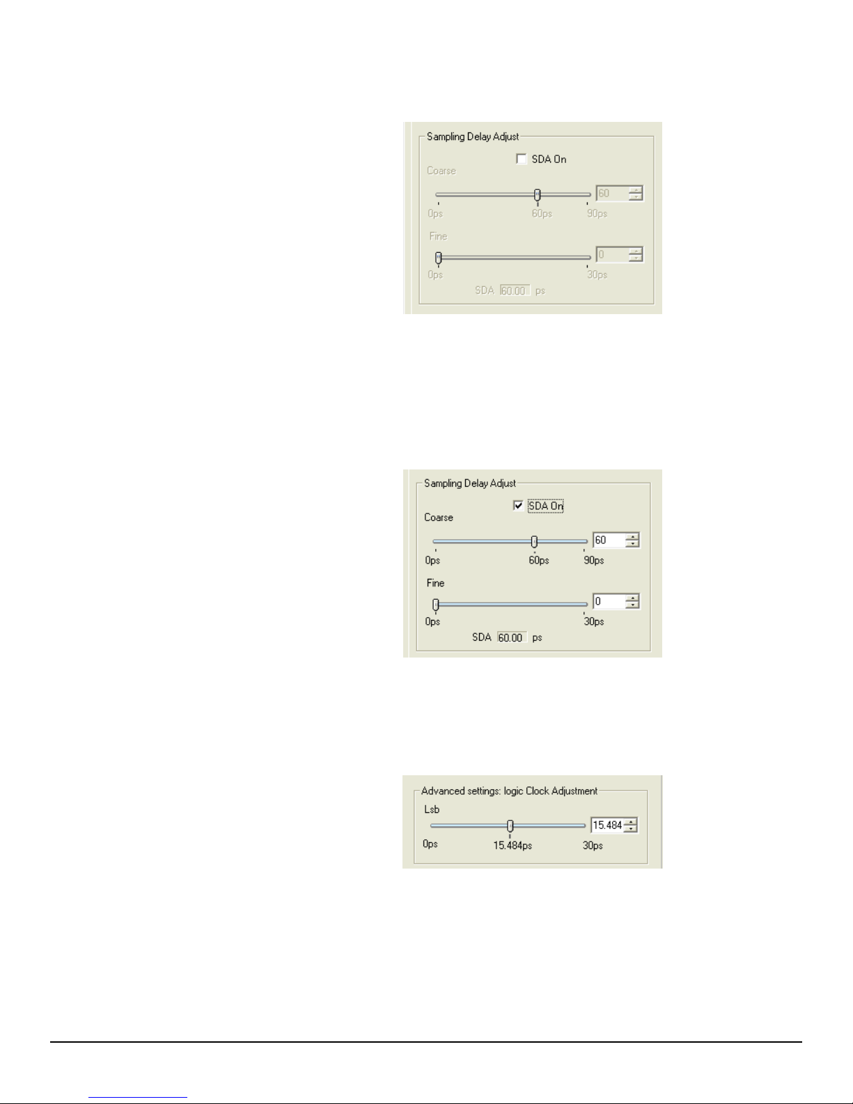
4.4.7 Sampling Delay
Adjust
Sampling Delay Adjustment Off
– Sampling delay adjustment On
– Coarse adjustment: 0 to 90 ps by step of 30 ps
– Fine adjustment: 0 to 30 ps by step of 0.118 ps
– Maximum delay: 120 ps
4.4.8 Advanced Setting:
Internal logic clock adjustment 0 to 30 ps on Lsb register
Logic Clock
Adjustment
EV10AS150A-EB User Guide 4-11
e2v semiconductors SAS 2009
0977B–BDC–10/09
Page 28

Software Tools
4.4.9 Clock Duty Cycle
(Track - Hold)
ADC Duty Cycle (Track-Hold): 40%-60% to 30%-70%
Note: Reset value 35%-65%
4-12 EV10AS150A-EB User Guide
0977B–BDC–10/09
e2v semiconductors SAS 2009
Page 29
Section 5
Application Information
5.1 Introduction For this section, refer also to the product chapter 4 of the datasheet.
5.2 Analog Inputs The analog input can be entered either single ended or differentially. Refer to the
datasheet to see the impact on dynamic performances.
It is recommended to use a filter to optimize the dynamic performance and the spectral
response of the ADC.
5.3 Clock Inputs The clock inputs should be differentially driven using a balun or hybrid junction.
The clock input is AC coupled.
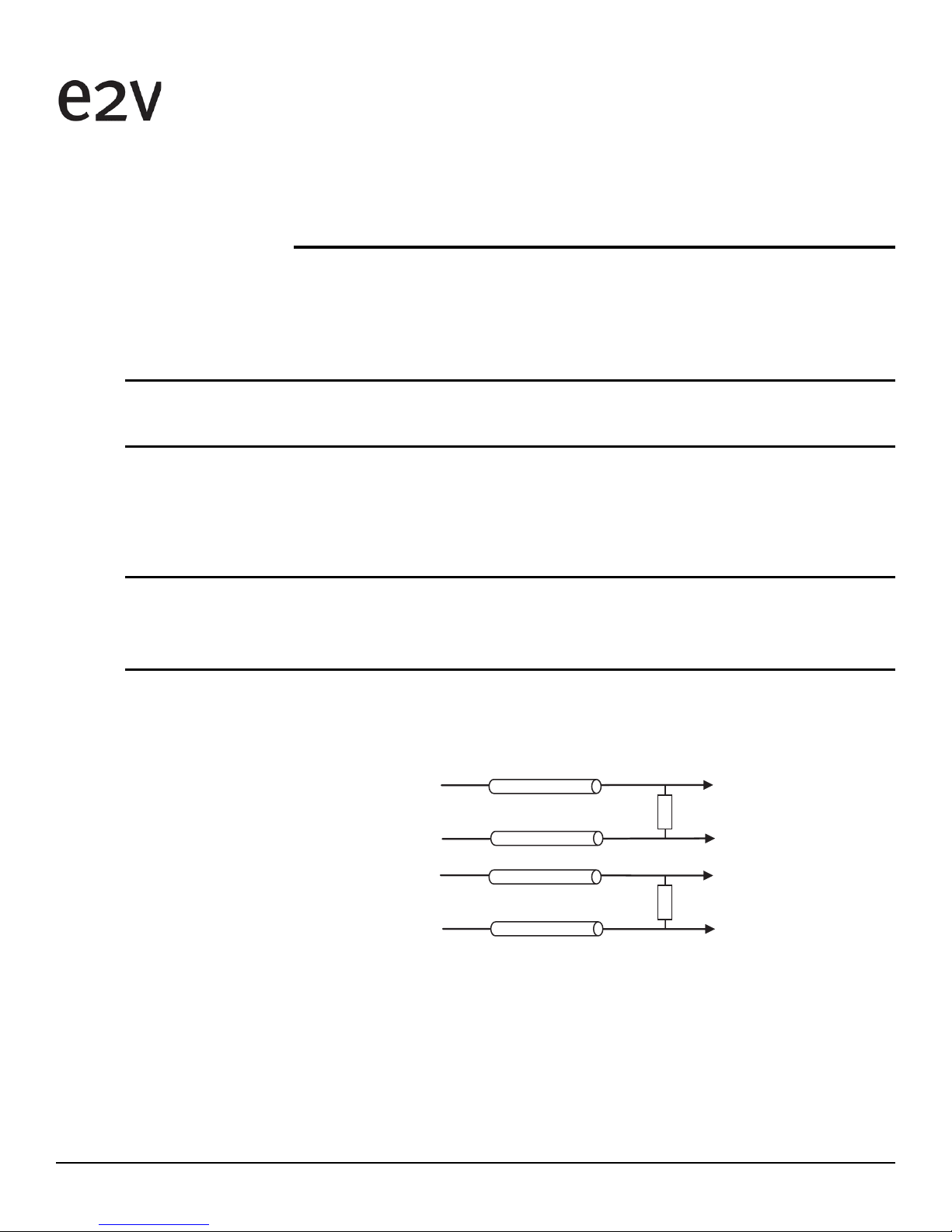
5.4 Digital Outputs The digital outputs (data and Data Ready) are LVDS compatible. 100Ω differential termi-
nation is provided on-board.
Figure 5-1. Differential Digital Outputs Implementation
Line
50Ω
50Ω
50Ω
50Ω
Line
Line
Line
100Ω
100Ω
Di
DiN
DRN
DR
EV10AS150A-EB User Guide 5-1
e2v semiconductors SAS 2009
0977B–IMAGE–10/09
Page 30
Application Information
5.5 ADC Functions
5.5.1 DRR (Data Ready
Reset)
The Data Ready Reset signal is accessed via an SMA connector.
DRR is CMOS/LVCMOS compatible:
V
= 0 (typical)
IL
V
IH
= V
CCA3
(typical)
The active level depends on the Data Ready Reset of 3WSI function (refer to section
4.4.2)
This signal acts as an internal Reset of the device. It is not mandatory for proper operation of the device. It is only used to determine exactly the first data to be sampled.
When applied, the clock outputs are Reset. The Reset pulse should last at least 3.5 ns.
An asynchronous Reset (ASYNCRST push button) should be applied while DRR is
active (high) in order to Reset properly the whole device.
In most cases (single channel application, no need to know which data will be the first
one to be sampled), this Reset can be left unused.
5.6 DMUX Functions
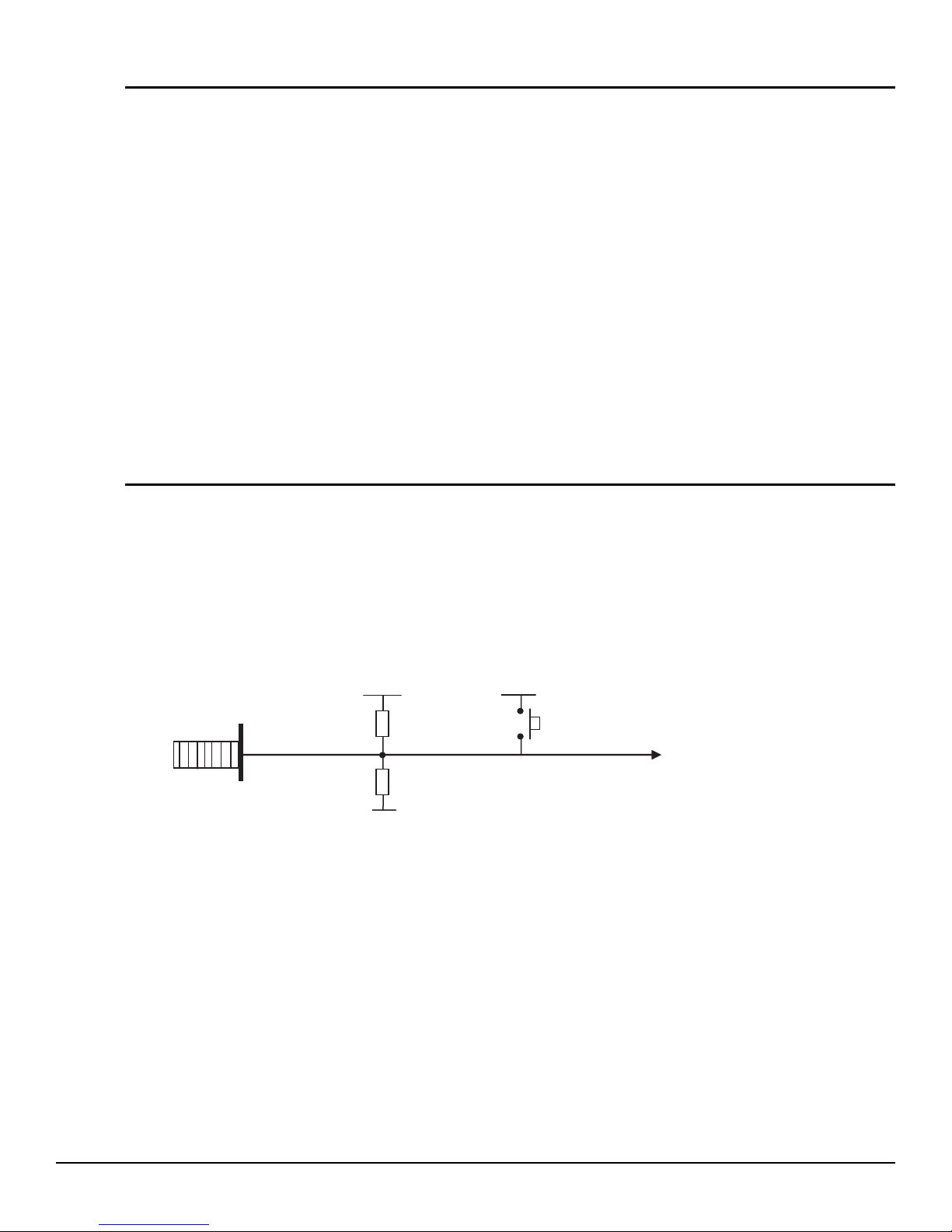
5.6.1 ASYNCRST The asynchronous Reset is mandatory to start the device properly. It should be applied
after power up of the device.
A push button is provided to perform this Reset and pull-up and pull-down resistors
allow to keep the ASYNCRST signal inactive.
Figure 5-2. ASYNCRST
3.3V
GND
15KΩ
4.7K
Ω
3.3V
ADC EV10AS150A
If the DRR Reset is also used, it is recommended to apply the asynchronous Reset
while the DRR Reset is active.
The first data is available at the device output after TOD + N cycles (with 4.5 ≤ N ≤ 7.5
depending on DEMUX mode).
5-2 EV10AS150A-EB User Guide
0977B–IMAGE–10/09
e2v semiconductors SAS 2009
Page 31
Application Information
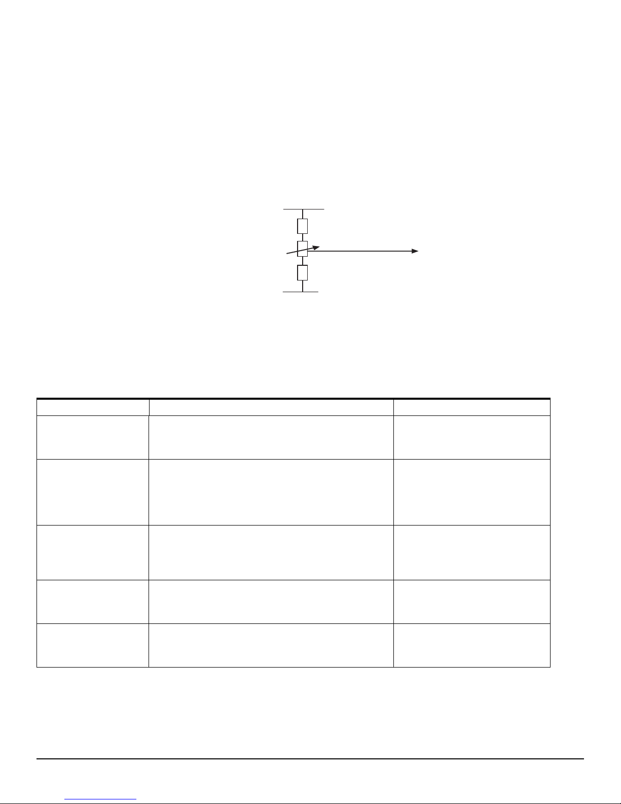
5.6.2 CLKDACTRL A delay cell is provided to allow the user to tune the delay between the Clock and Data
at the DMUX input. The delay is controlled via the CLKDACTRL potentiometer.
This cell allows you to delay the internal DMUX clock via the CLKDACTRL potentiometer (varying from V
/3 to (2 x V
CCD
CCD
)/3).
This pin must be biased and it is recommended to set CLKDACTRL at VCCD/3. With
this value it is normally not necessary to tune CLKDACTRL voltage over the full specified clock rate.
Figure 5-3. CLKDACTRL Potentiometer
3.3V
kΩ
10
kΩ
10
10
Ω
k
GND
ADC EV10AS150A
5.6.3 RS, DRTYPE, BIST,
SLEEP, STAGG
Seven jumpers are provided for the RS, DRTYPE, BIST, SLEEP and STAGG functions.
Table 5-1 describes each function.
Table 5-1. DMUX Function Settings and Description
Function Description Jumper Settings
Ratio selection:
RS
DRTYPE
BIST
SLEEP
STAGG
- 1:2
- 1:4
Output clock mode:
- DR = data valid on each rising edge of the DR/DRN
signal
- DR/2 = data valid on both rising and falling edges of the
DR/DRN signal
Built-In Self Test:
- Active: checker board pattern available at the device
outputs
- BIST inactive: normal mode
Sleep mode
- Active: the device is in a partial standby mode
- SLEEP inactive: normal mode
Simultaneous or Staggered output mode
- STAGG active: staggered output data
- STAGG inactive: simultaneous output data
1:2: Jumper ON
1:4: Jumper OUT
DR: Jumper OUT
DR/2: Jumper ON
BIST: Jumper ON
No BIST: Jumper OUT
SLEEP: Jumper ON
SLEEP inactive: Jumper OUT
STAGG: Jumper ON
STAGG inactive: Jumper OUT
EV10AS150A-EB User Guide 5-3
e2v semiconductors SAS 2009
0977B–IMAGE–10/09
Page 32
Application Information
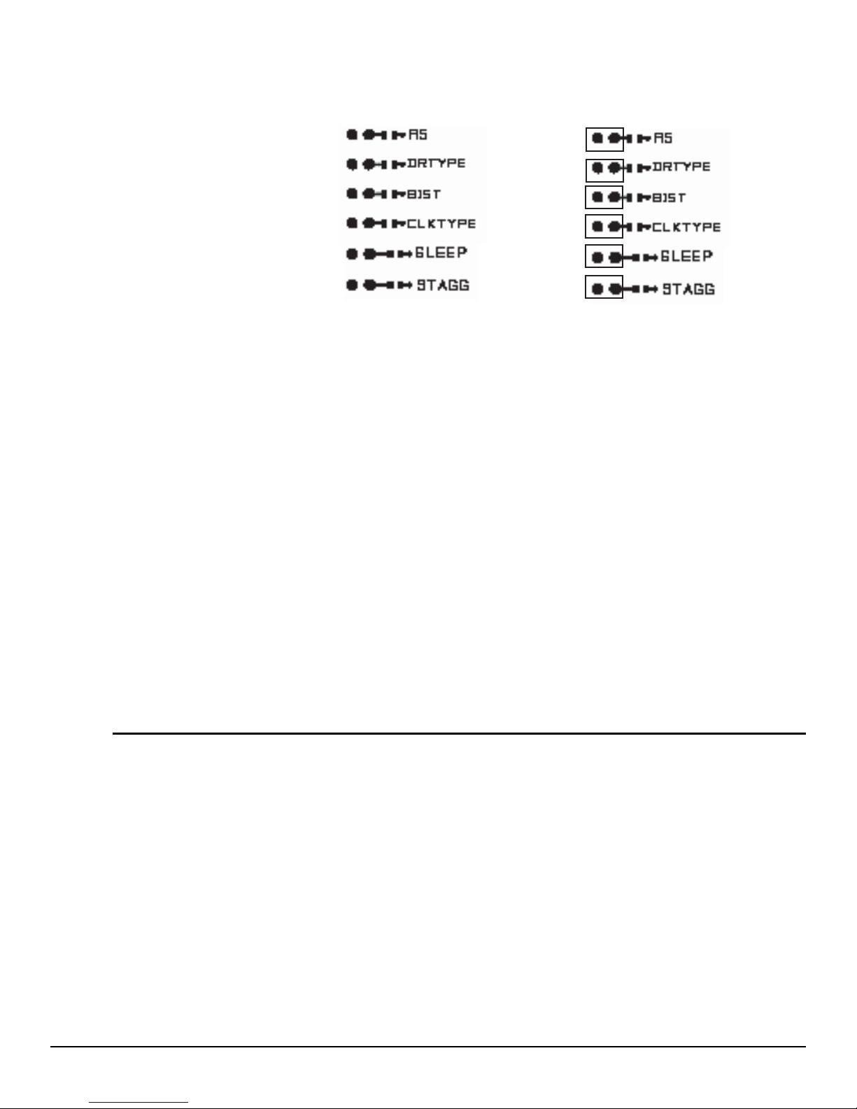
Figure 5-4. DMUX Functions Jumper Positions
Jumper OUT Jumper ON
Jumper CLKTYPE can be placed in any position: it has no effect.
5.6.4 Additional OR Bits In simultaneous mode, the out-of-range signal of the ADC is demultiplexed by the
DMUX and output on all ports as the (AOR/DRAN, AORN/DRA), (BOR/DRBN,
BORN/DRB), (COR/DRCN, CORN/DRC) and (DOR/DRDN, DORN/DRD) signals.
These signals can be used to detect if the input of the ADC is above the full scale.
In staggered mode, these signals correspond to the output clock for each port:
DRA, DRAN for Port A (pins A6, B6)
DRB, DRBN for Port B (pins J2, H1)
DRC, DRCN for Port C (pins W5, V5)
DRD, DRDN for Port D (pins W17, V17)
5.7 Diode for Die
Junction
Temperature
Monitoring
Two diodes for die junction temperature measurement are available, for maximum junction temperature monitoring (hot point measurement) of both the ADC and the DMUX.
The measurement method consists in forcing a 1 mA current into a diode mounted
transistor.
The measurement setup is described in Figure 5-5.
5-4 EV10AS150A-EB User Guide
0977B–IMAGE–10/09
e2v semiconductors SAS 2009
Page 33
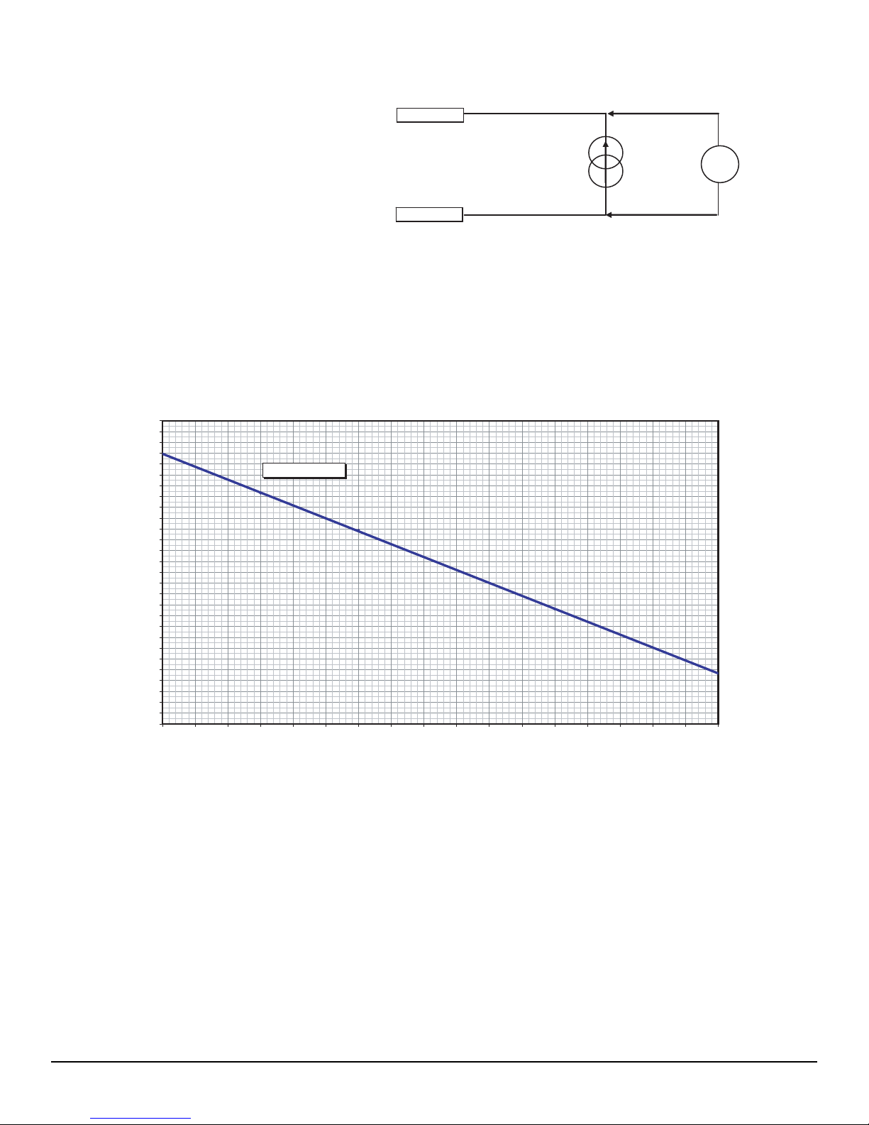
Figure 5-5. ADC DIODE Measurement Setup
IGND
Application Information
Note: The 1 mA current can be supplied by a multimeter set in this specific current source
Figure 5-6. ADC DIODE Characteristics
Junction
980
970
960
950
940
930
920
910
900
890
880
870
860
850
840
830
820
810
Diode voltage (mV)
800
790
780
770
760
750
740
730
720
710
700
-30 -20 -10 0 10 20 30 40 50 60 70 80 90 100 110 120 130 140
y = -1.193x + 913.714
1 mA
V
Idiode
mode: in this case, the voltage measured between the diode pin and ground is displayed
on the multimeter.
T
emperature versus Diode Voltage for I = 1mA
Junction temperature (°C)
EV10AS150A-EB User Guide 5-5
e2v semiconductors SAS 2009
0977B–IMAGE–10/09
Page 34
Application Information
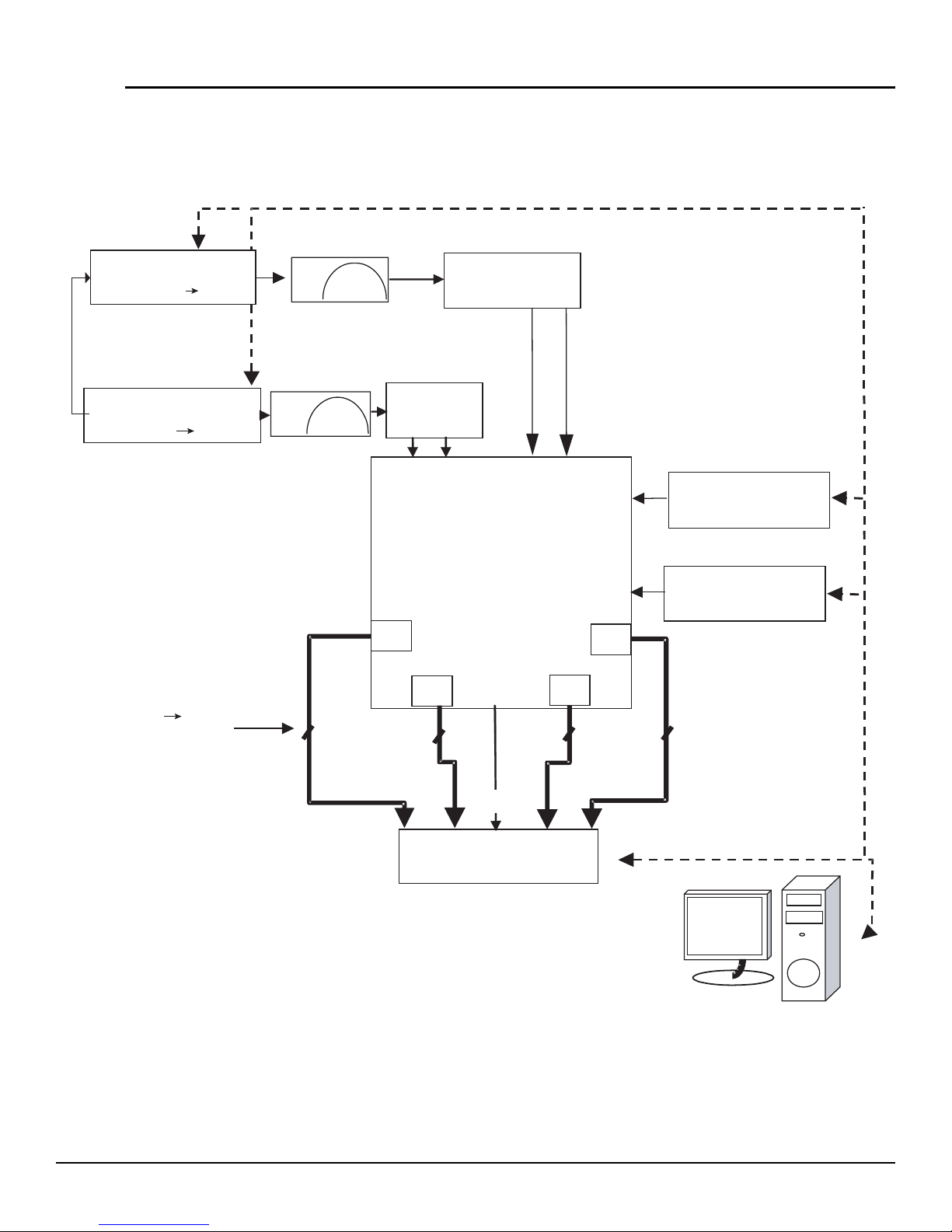
5.8 Test Bench
Description
Figure 5-7. Test Bench Description
Wave
HP8665B
Signal Sour ce
Signal generator is
locked with the
clock generator
Sine-
Fin
phase
BPF
Balun
Macom -
H9
0˚C 180˚C
HP8665B Sine-Wave
Clock Source Fs
Acquisition board
Acquisition board
D0 D9
*
4 Channel
Balun
BPF
180˚C
Ana r en
0˚C
Fs = ADC sampling data
Power supplies
GW PPT
EV10AS150A
Power supplies
A
B
Clock
HP16500C
Analysis Logic
C
D
GW PPT
GPIB Bus
5-6 EV10AS150A-EB User Guide
0977B–IMAGE–10/09
LabView
e2v semiconductors SAS 2009
Page 35
6.1 Thermal
Characteristics
Section 6
Package Information
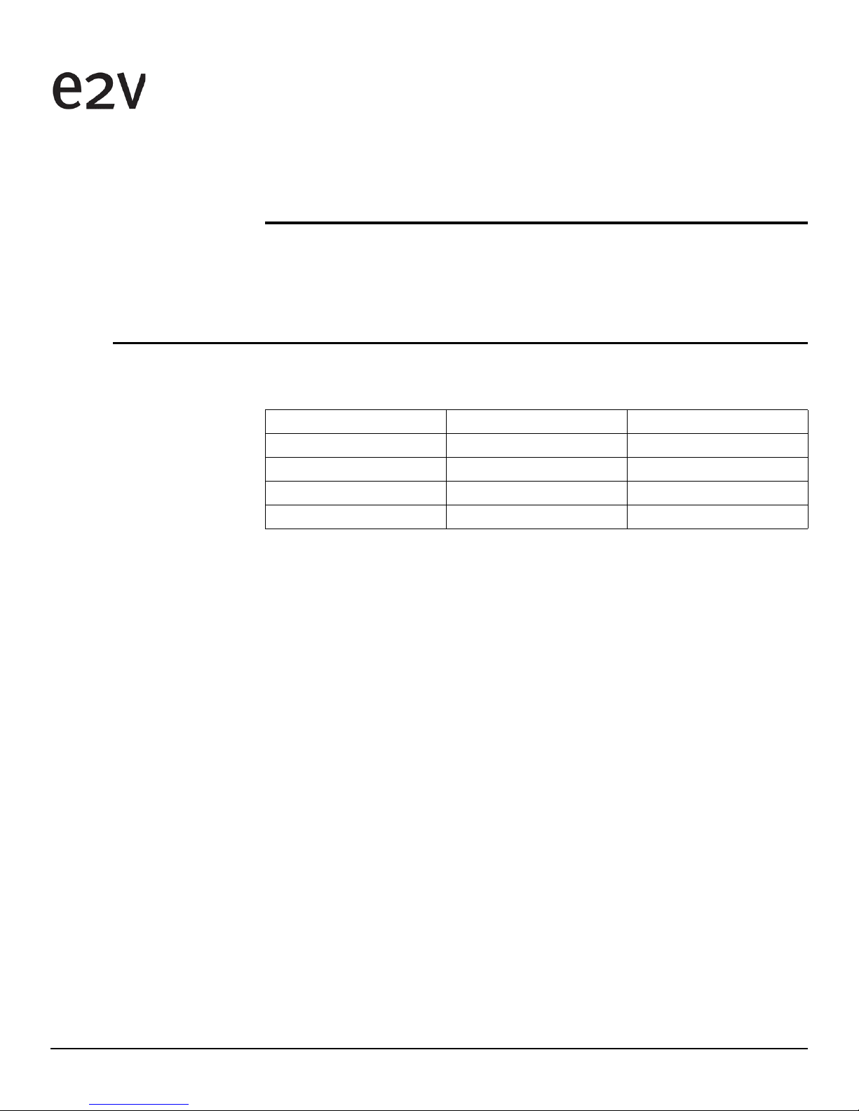
Table 6-1. Thermal Resistance (No air, pure conduction, no radiation)
Thermal Resistance ADC Alone DMUX Alone
RTHj-top-of-case 4.11 °C/Watt 1.48 °C/Watt
RTHj-bottom-of-balls 6.94 °C/Watt 3.89 °C/Watt
RTHj-board 7.98 °C/Watt 4.88 °C/Watt
RTHj-ambient 17.13 °C/Watt 13.88 °C/Watt
Note: No external heatsink is mandatory.
EV10AS150A-EB User Guide 6-1
e2v semiconductors SAS 2009
0977B–BDC–09/09
Page 36

Package Information
6-2 EV10AS150A-EB User Guide
0977B–BDC–09/09
e2v semiconductors SAS 2009
Page 37

Ordering Information
Part Number Package Temperature Range Screening Comments
For availability, contact your local
EV10AS150ATP-EB EBGA 317 Ambient Prototype
EV10AS150ACTP EBGA 317 Commercial grade T
EV10AS150AVTP EBGA 317 Industrial grade T
Commercial grade
EV10AS150ACTPY EBGA 317
EV10AS150AVTPY EBGA 317
RoHS T
Industrial grade
RoHS T
> 0°C, TJ < 90°C
amb
> –40°C, TJ < 110°C
amb
> 0°C, TJ < 90°C
amb
> –40°C, TJ < 110°C
amb
e2v sales office.
For availability, contact your local
e2v sales office.
For availability, contact your local
e2v sales office.
For availability, contact your local
e2v sales office.
For availability, contact your local
e2v sales office.
Section 7
EV10AS150A-EB User Guide 7-1
e2v semiconductors SAS 2009
0977B–BDC–10/09
Page 38

Ordering Information
7-2 EV10AS150A-EB User Guide
0977B–BDC–10/09
e2v semiconductors SAS 2009
Page 39

8.1 EV10AS150A-EB Electrical Schematics
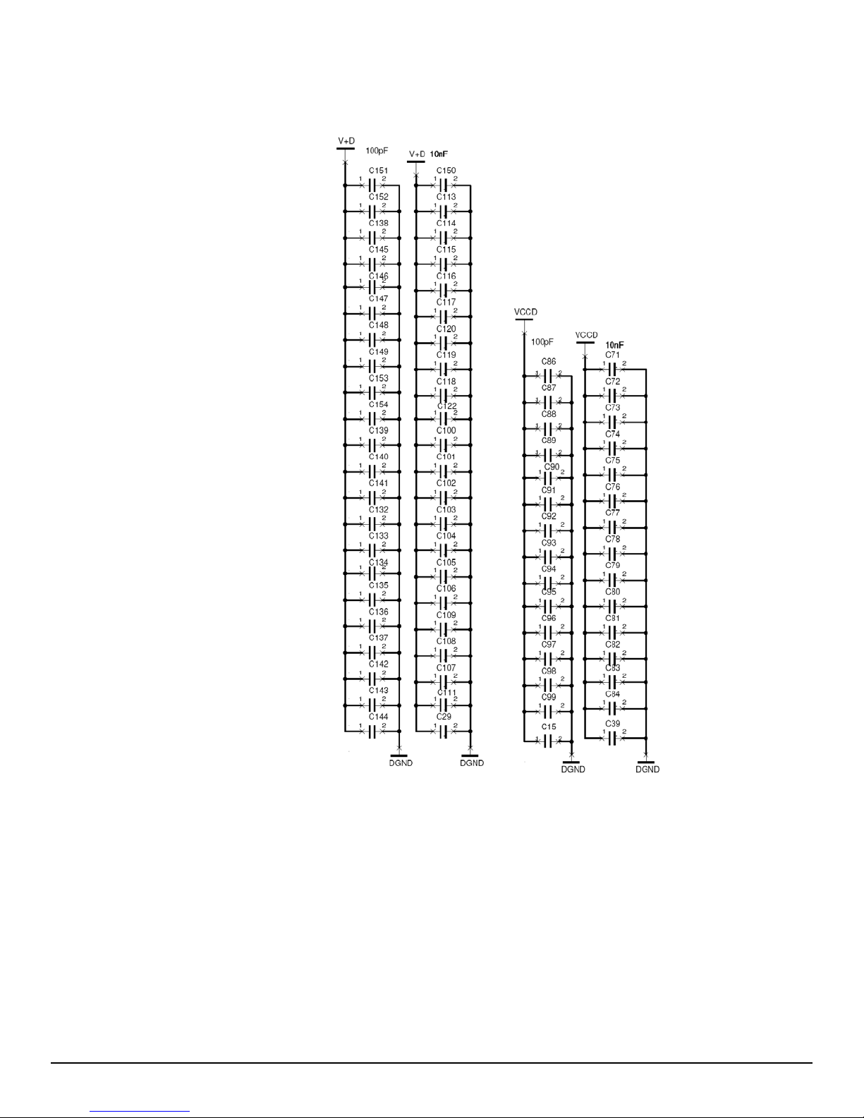
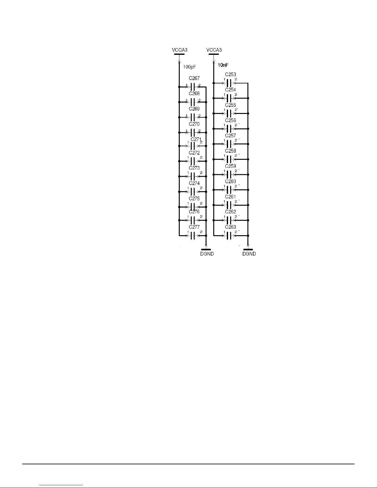
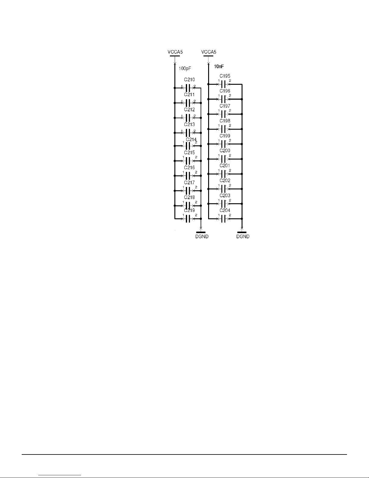
Note: For ADC decoupling strategy, please do not take into account the current
decoupling implemented on current evaluation board which is purely experimental. Refer to Datasheet for recommended decoupling strategy.
Section 8
Appendix
EV10AS150A-EB User Guide 8-1
e2v semiconductors SAS 2009
0977B–BDC–10/09
Page 40
Appendix
D
PIN V+D
Figure 8-1. Decoupling PIN
ecoupling
Decoupling PIN VCCD
8-2 EV10AS150A-EB User Guide
0977B–BDC–10/09
e2v semiconductors SAS 2009
Page 41
Appendix
Figure 8-2. Decoupling PIN V
CCA3
EV10AS150A-EB User Guide 8-3
e2v semiconductors SAS 2009
0977B–BDC–10/09
Page 42
Appendix
Figure 8-3. Decoupling PIN V
CCA5
8-4 EV10AS150A-EB User Guide
0977B–BDC–10/09
e2v semiconductors SAS 2009
Page 43
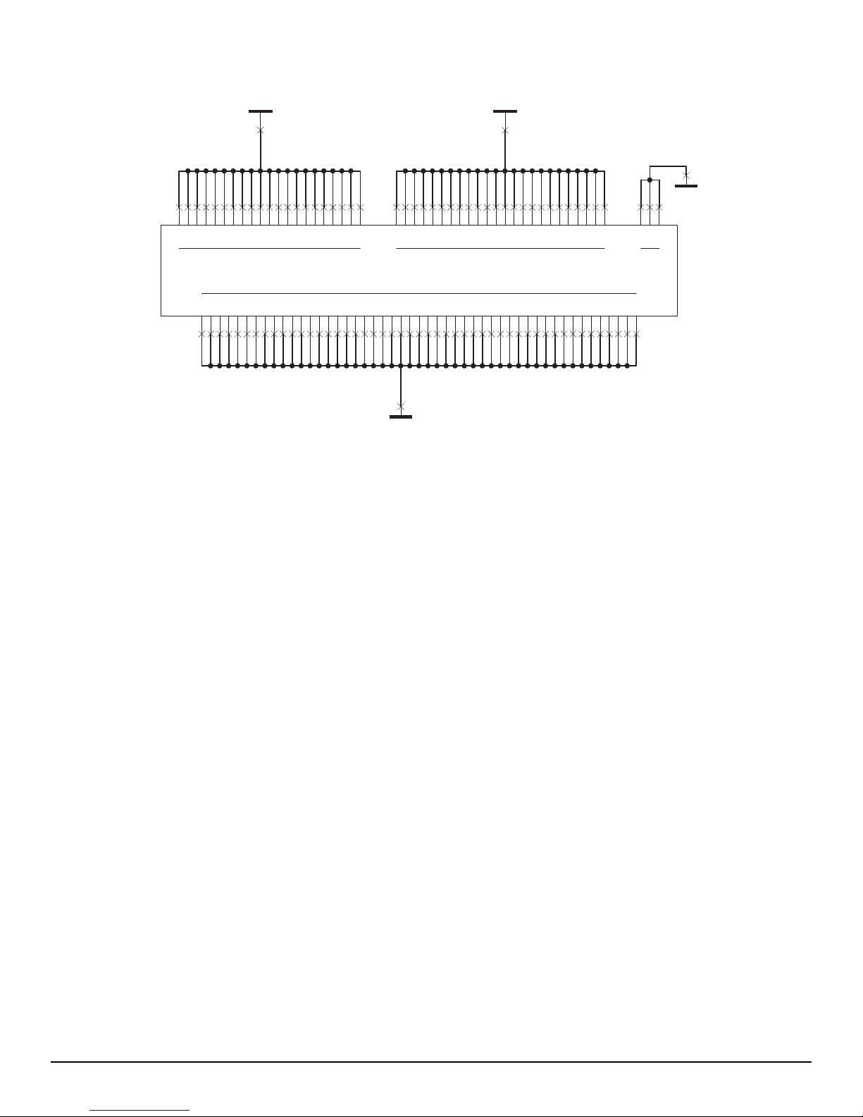
Figure 8-4. Power Supplies Connections
Appendix
VCCA3VCCA5
.EV10AS150A
C27
B27
A27
3/3
C26
A26
D27
M27
B26
D26
L26
L25
C24
D24
R21
T21
E24
B24
A24
F25
E26
VCCA3 VCCA3
F27
U27
V27
T27
K27
G27
R27
W27
F26
G26
H26
J26
R26
T26
U26
V26
W26
G25
MN6-C
DG ND
F20
M25
D22
U21
L27
N27
K26
M26
N26
A25
B25
C25
D25
E25
AGND
N25
J25
P25
H25
DGND
W25
U25
T25
R25
B23
V24
U24
T24
R24
C22
K25
F24
B22
T23
R23
F23
E23
D23
C23
E20
F22
C20
E22
R22
V23
U23
T20
R20
D20
D21
C21
B21
W22
U22
T22
R17
D14
D15
SUB
V21
F21
E21
EV10AS150A-EB User Guide 8-5
e2v semiconductors SAS 2009
0977B–BDC–10/09
Page 44
Appendix
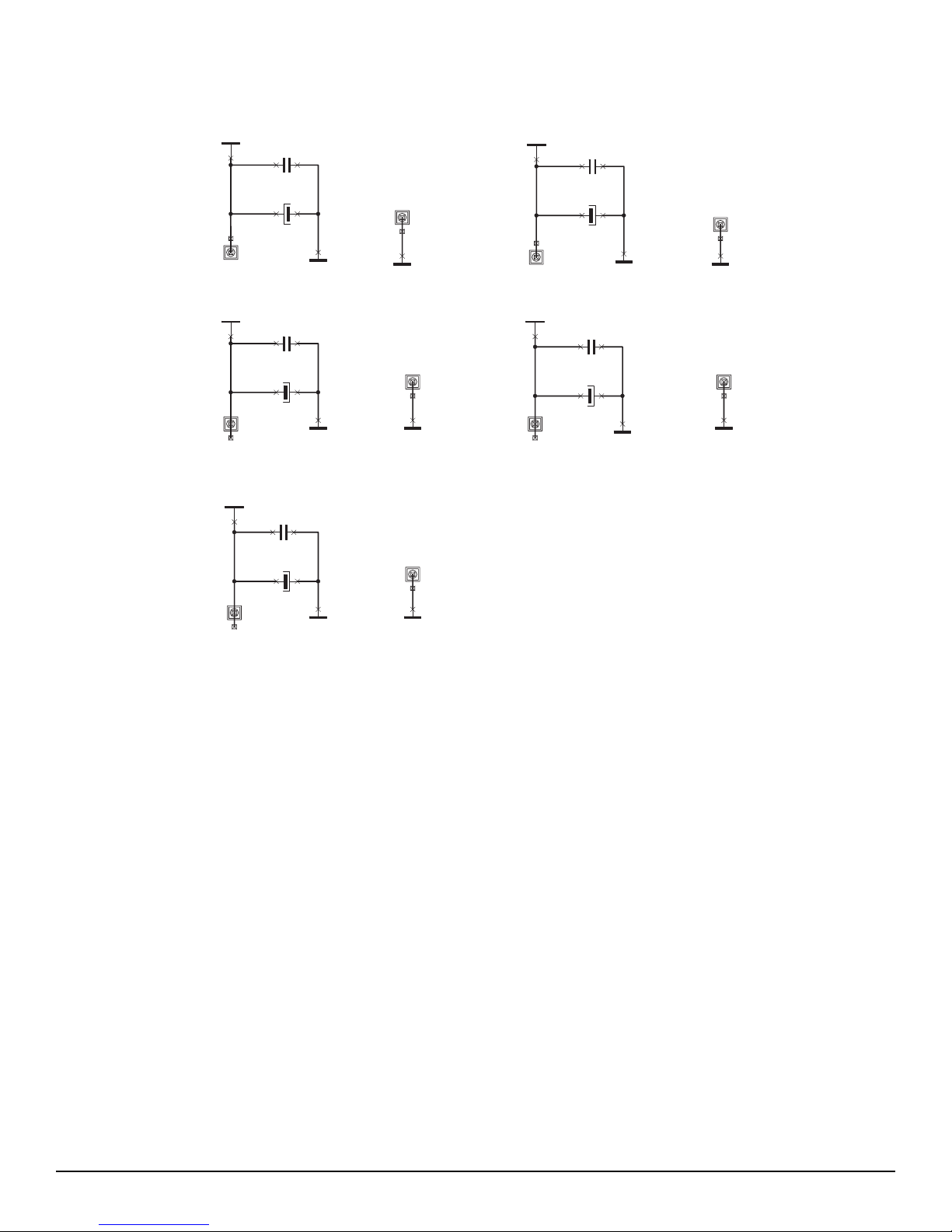
Figure 8-5. Power Supplies Bypassing
J32
J41
J45
VCCA3
2
1
V+D
1
2
VCCD
1
2
C69 100nF
1
C70 1uF
2
C4 100nF
1
C2 1uF
1
2
C3 100nF
1
2
C1 1uF
1
2
2
1
2
DGND
DGND
DGND
J49
1
2
DGND
1
2
DGND
1
2
DGND
J20
J23
J27
J42
3V3
2
1
VCCA5
1
2
C5 100nF
1
2
C6 1uF
1
2
C66 100nF
1
2
C65 1uF
1
2
DGND
DGND
J30
1
2
DGND
1
2
DGND
J26
8-6 EV10AS150A-EB User Guide
0977B–BDC–10/09
e2v semiconductors SAS 2009
Page 45
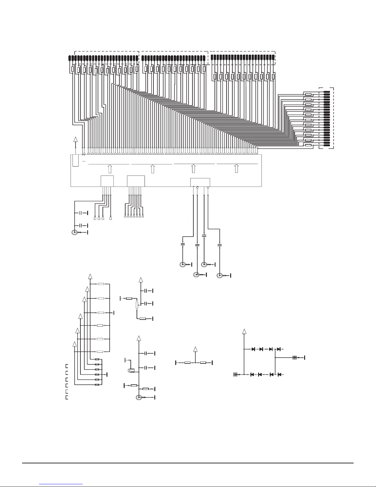
Figure 8-6. EV10AS150A-EB Electrical Schematic (ADC DMUX)
J4
J6
J6
TO P
G-4pts
G-4pts
3
.
.
.
.
.
2
23
22
S-2R
S-2R
2
2
1%
14-MD
14-MD
HE
HE
1
1
R= 100 ohm
R1
R45
DR
DRN
A0-
DIODE-ADC
W2 1
C
DIODEAD
L
OUTPUT
CONTRO
MN6-A
EV10AS15x
J4
J4
J4
J4
J4
J4
J5
J5
J5
J5
J5
J5
J5
J5
J5
J5
J5
J5
J5
J5
J5
J5
J5
.
.
.
.
.
.
.
.
.
.
20
19
21
2
2
1
1
R2
R3
+
A0
A1-
A1+
.
.
18
15
14
13
17
16
12
11
2
2
2
1
1
1
R5
R4
R6
A3-A3+
A4-
A5-
A2-
A5+
A2+
A4+
J5
.
.
.
.
.
.
9
10
8
6
4
7
5
2
2
2
2
1
1
1
1
R7
R9
R10
R8
A6-A6+
A7-
A7+
A8-
A8+
A9-
J4
J5
J5
J4
J5
J5
.
.
.
.
.
.
.
21
3
2
20
23
22
2
1
1
HE 14-MDS-2RG-24pts
HE 14-MDS-2RG-24pts
HE 14-MDS-2RG-24pts
HE 14-MDS-2RG-24pts
HE 14-MDS-2RG-24pts
HE 14-MDS-2RG-24pts
HE 14-MDS-2RG-24pts
HE 14-MDS-2RG-24pts
HE 14-MDS-2RG-24pts
HE 14-MDS-2RG-24pts
HE 14-MDS-2RG-24pts
HE 14-MDS-2RG-24pts
HE 14-MDS-2RG-24pts
HE 14-MDS-2RG-24pts
HE 14-MDS-2RG-24pts
HE 14-MDS-2RG-24pts
HE 14-MDS-2RG-24pts
HE 14-MDS-2RG-24pts
HE 14-MDS-2RG-24pts
HE 14-MDS-2RG-24pts
HE 14-MDS-2RG-24pts
HE 14-MDS-2RG-24pts
1
2
2
R11
R12
R13
1%
N
A0RN/DRA
100ohm
AOR/DRA
R=
+
B0-
B0+
B1-B1
A9+
.
J1
A15
B16
A16
K2
A0
A0N
DR
DRN
DATA READY
1/3
A10
B11
A11
A12
B13
A13
B14
A14
B15
B12
A3
A1
A4
A2
A1N
A4N
A3N
A2N
CONTROL
C
SCLK
RESET
DRR
AD
A22
P27
E27
A9
A5
A8
A8NA7A7NA6A6N
A9NB7B0N
CONTROL
DMUX
N
AORN/DRA
AOR/DRA
ASYNCRST
B17L2K1
A5N
A
DATA
SDATA
SLDN
A21
A23
C2R1B1
B2B3B4B5B6B7A2A3A4A5A6A7B8A8B9A9B10
N
B0
B1
B5
B4
B3
B2
B5
B1N
B3NC3B4N
B2N
DATA B
CLKDACTRLBISTRSDRTYPE
STAGG
SLEEP
U18
V17
A17
A18
J4
J4
J4
J4
J4
J4
J4
J4
J4
J4
.
.
18
19
1
2
R14
B2-
B2+
B6
B6N
B7NB8
J4
J4
.
.
.
.
.
.
.
.
14
1
R16
+
B4-
B4
B9
BORN/DRB
.
13
N
BOR/DRB
.
.
7
8
6
12
11
10
9
1
1
1
1
2
2
2
2
R17
R18
R19
R20
B8-
B5-
B8+
B5+
B6-
B6+
B7-B7+
R2
P2
C4
C2
C1
C0
C4NC6C5N
C2N
C3N
C1N
DATA C
K
INPUTS
CL
W2 4
.
16
15
17
B3
1
2
2
R15
B3+
N
B9NB8C0N
Appendix
J3
J3
J3
J3
J3
J3
J3
.
.
.
.
.
19
18
17
16
+
C3
C2-
C2+
C3-
12
12
12
R26
R25
V10
W10V9W9V8W8V7W7V6W6V5W5V4W4V3W3V2W2V1U1U2T1T2P1N1N2M1M2L1J2H1H2G1G2F1F2E1E2D1D2C1
D1
D2
D4ND3D3N
D1N
D2N
J3
.
.
.
15
14
13
C4-C4+
C5-C5+
12
R27
1
W1 2
V11
W1
D5
D4
D5N
D6ND6D8N
D
DATA
J3
J4
.
.
.
.
.
.
.
4
5
2
R21
B9-
C5
C6N
KN
CL
W2 3
21
2
1
2
2
R2
BORN/DRB
N
VI
H27
N
BOR/DRB
C8
C8NC7C7N
J27
HE 14-MDS-2RG-24pts
HE 14-MDS-2RG-24pts
HE 14-MDS-2RG-24pts
HE 14-MDS-2RG-24pts
HE 14-MDS-2RG-24pts
HE 14-MDS-2RG-24pts
HE 14-MDS-2RG-24pts
HE 14-MDS-2RG-24pts
HE 14-MDS-2RG-24pts
HE 14-MDS-2RG-24pts
HE 14-MDS-2RG-24pts
HE 14-MDS-2RG-24pts
HE 14-MDS-2RG-24pts
HE 14-MDS-2RG-24pts
HE 14-MDS-2RG-24pts
HE 14-MDS-2RG-24pts
HE 14-MDS-2RG-24pts
HE 14-MDS-2RG-24pts
HE 14-MDS-2RG-24pts
HE 14-MDS-2RG-24pts
HE 14-MDS-2RG-24pts
HE 14-MDS-2RG-24pts
R= 100ohm 1%
VINN
23
22
C0-
C0+
C1-
12
R23
C9
D0N
C9N
CORN/DRC
COR/DRCN
20
+
C1
R24
D0
3
1
B9+
J3
J3
J3
J3
.
.
.
.
9
10
11
12
C6-
C7-
C6+
12
12
R28
R29
W1 5
V14
W1 4
V13
W13V12
D7
D8
D7N
D9N
J3
J3
J3
J3
.
.
.
7
8
6
+
C7
C8-
C8+
12
12
R30
R31
V16
W1 6
V15
D9
DORN/DRD
DOR/DRDN
J3
J3
J3
J3
.
J3
3
4
5
2
C9-
C9+
CORN//DRC
COR/DRCN
12
12
2
R3
R33
TO P
HE 14-MDS-2RG-24pts
HE 14-MDS-2RG-24pts
HE 14-MDS-2RG-24pts
HE 14-MDS-2RG-24pts
HE 14-MDS-2RG-24pts
HE 14-MDS-2RG-24pts
HE 14-MDS-2RG-24pts
HE 14-MDS-2RG-24pts
HE 14-MDS-2RG-24pts
HE 14-MDS-2RG-24pts
HE 14-MDS-2RG-24pts
HE 14-MDS-2RG-24pts
HE 14-MDS-2RG-24pts
HE 14-MDS-2RG-24pts
HE 14-MDS-2RG-24pts
HE 14-MDS-2RG-24pts
HE 14-MDS-2RG-24pts
HE 14-MDS-2RG-24pts
HE 14-MDS-2RG-24pts
HE 14-MDS-2RG-24pts
HE 14-MDS-2RG-24pts
HE 14-MDS-2RG-24pts
HE 14-MDS-2RG-24pts
HE 14-MDS-2RG-24pts
HE 14-MDS-2RG-24pts
HE 14-MDS-2RG-24pts
HE 14-MDS-2RG-24pts
HE 14-MDS-2RG-24pts
HE 14-MDS-2RG-24pts
HE 14-MDS-2RG-24pts
HE 14-MDS-2RG-24pts
HE 14-MDS-2RG-24pts
HE 14-MDS-2RG-24pts
HE 14-MDS-2RG-24pts
HE 14-MDS-2RG-24pts
HE 14-MDS-2RG-24pts
HE 14-MDS-2RG-24pts
HE 14-MDS-2RG-24pts
HE 14-MDS-2RG-24pts
HE 14-MDS-2RG-24pts
HE 14-MDS-2RG-24pts
HE 14-MDS-2RG-24pts
HE 14-MDS-2RG-24pts
TO P
R= 100 ohm 1%
R34
R35
R36
R37
8
R3
R39
R40
R4
1
2
R4
R4
3
.
.
J2
23
D0-
.
2
1
D0+
22
.
J2
21
D1-
.
2
1
2
1
2
1
2
1
2
1
2
1
2
1
2
1
2
1
2
1
R44
D1+
D2-
D2+
D3-
D3+
D4
D4+
D5-
D5+
D6-
D6+
D7-
D7+
D8-
D8+
D9-
D9+
RN/DRD
DOR/DRDN
J2
20
.
J2
19
.
J2
18
.
J2
17
.
J2
16
.
J2
15
.
J2
14
.
J2
13
.
J2
12
.
J2
11
.
J2
10
.
J2
9
.
J2
8
.
J2
7
.
J2
6
.
J2
5
.
J2
4
.
J2
3
DO
J2
2
J2
DRR
C314NE10nF
1
2
DG NDDGNDDG
NE
C313
100pF
1
2
.
1
2
3
J10-A
A
LK
DN
SC
SL
SDAT
R ESET
ND
CLKTYPE
R63
10K
BIST
RS
DRTYPE
G
STAG
EEP
SL
DMUX CONTRO L
.
.
SW 7
.
.
SW 6
.
SW5
.
SW4
3
SW
2
SW
(X6)
NE
2
1
1
R6
NE
10K
2
1
R62
1
R60
1
R59
1
R64
1
J13
1
2
1
J1
1
2
4
J1
1
2
J15
1
2
6
J1
1
2
9
J3
1
2
3V3
2
10K
NE
2
DGND
10K
NE
2
10K
NE
2
10K
NE
2
.
.
.
.
.
.
3V3
B
.
HUB
TTSK
ND
CH-S
DG
IT
SW
3V3
T
EEP
SL
ASYNCRS
10K
R48
R53
1
SW 1
15K
R55
2
G
STAG
10K
3
J18-A
DRTYPE
1
4
2
.
RS
10nF
12
3
1
ASYNCRST
10nF
1
123
L
BIST
KDACTR
CL
L
CLKDACTR
312
C
1
C310
1
R49
10K
C309
1
C8
100pF
1
2
R5
1
2
100pF
2
2
2
2
4.7K
VI N
VINN
CLK
CLKN
12
C321 100pF
12
C320 100pF
.
J33-A
12
319 100pF
C
.
1
2
3
DG ND
.
A
1
J34-
12
C322 100pF
1
2
3
DG ND
J8-A
.
1
J9-A
2
3
DGND
2
3
DG ND
ND
.
DG ND DG
DG ND
DIODE- ADC
9
CR3
BAV99
CR4
C
DACTRL
ND
DG
DELAY ELL
3
3V
1
R50
R5
10K
10K
1
2
1
2
DGND
DG ND
J21
DGNDDG
2
1
CR1
2
1
BAV9
2
3
123
J22
DGND
1
2
E
CR2
BAV99
BAV99
123
123
ND
EV10AS150A-EB User Guide 8-7
e2v semiconductors SAS 2009
0977B–BDC–10/09
Page 46
Appendix
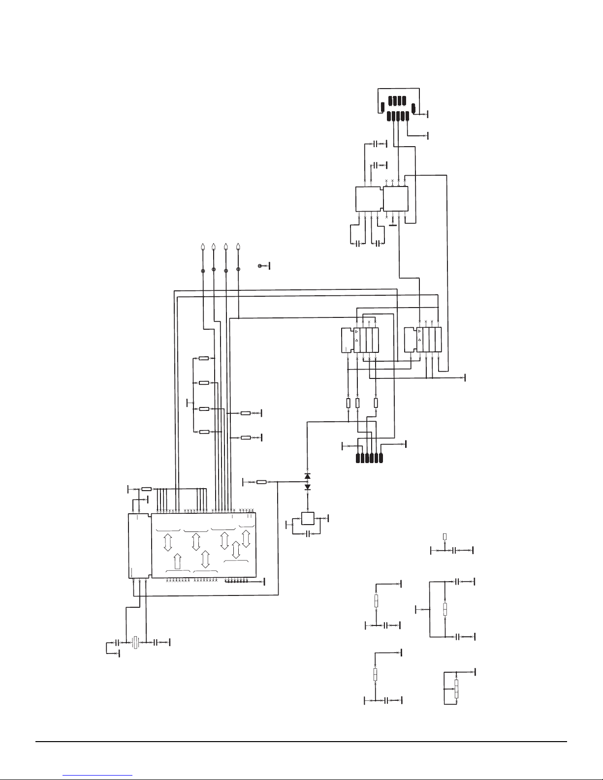
Figure 8-7. EV10AS150A-EB Electrical Schematic (AVR)
A
PT19
ESET
R
1
PT11
SCLK
SDAT
SLDN
ND
1
1
1
1
PT18
PT17
PT12
DG
232
RS
LTC1386CS-PBF
9PTS
SUBD
A
MN3-
2
7
7
J17
J1
J1
J17
F
F
F
F
F
F
F
F
F
F
F
9
8
7
6
+
C1
1
7
J1
2
2
6
2
V-
V+
+
C2
C1-
4
3
10
.
.
D09P13A4GL00L
D09P13A4GL00L
D09P13A4GL00L
D09P13A4GL00L
D09P13A4GL00L
D09P13A4GL00L
D09P13A4GL00L
D09P13A4GL00L
D09P13A4GL00L
D09P13A4GL00L
D09P13A4GL00L
100nF
C68
1
4
100nF
C6
1
D
GN
1XVC C
1X
C2
5
.
9
8
7
.
J1
1
RX
ND
DG
DGND
7
RX2OUT
RX2IN
10
7
.
J1
.
3
2
TX
TR2OUT
TR2IN
J17
.
14
TR1OUT
TR1IN
11
7
J1
.
4
12
RX10OUT
RX1IN
13
11
7
J1
J17
ND
DG
5
ND
DG
DGND
1
1
2
100nF
C62
100nF
C60
9
7
5
SN74HC241
10nF
1
1
3
MN4-B
2
OE
11
13
15
17
19
ND
DG
ND
DG
.
D
V1
MN2-
64
ATMEGA128L
10nF
C123
ND
1
2
3V3
.
DGND
52
B
3
3V
ND
DG
ND
DG
ND
DG
MN2-
ATMEGA128L
V1 V2
.
21
DG
10nF
C121
2
1
DGND
10nF
C112
1
2
DGND
DGND
63
V3
C
53
MN2-
V1 V2
ATMEGA128L
22
12
14
16
18
C
SN74HC241
GND
A
XVC
1X
1
1
MN4-
1K
R82
.
1
2
P
0
1K
AKEU
R8
W
.
1
2
1K
R79
3V3
.
1
2
1K
R75
.
1
2
1K
R76
.
3
1
2
3V
DGND
1
62
C
D
C
PEN
AREF
GN
2XVC
XAVC
3X
1
MN2-A
µC
ATMEGA128L
2
1
RESET
XTAL
XTAL
23
24
20
22pF
C126
1
C127
2
2
1
2
ND
Y2
DG
6864 MHz
3.
32
2
3
4
5
6
7
8
9
1
0
T2
IN
-A
/PD0
/INT7
-INT4
3A
3B
3C-INT5
T3/INT6
IC3
RXD0/PDI
TXD0
OC
XCK0/AIN
OC
OC
0..7
DATA
PE
..7
0
ADR
PA
5
4
3
2
0
AD
AD
AD
AD
AD1
AD
45
46
47
48
49
50
51
22pF
1
DGND
16
17
25
26
27
28
29
30
31
1B
T1
IC1
/INT2
OC
OC1C
/INT0
XCK1
SDA/INT1
SCL
OC2/
TXD1/INT3
RXD1
0..7
DATA
PD
0..7
ADR
PC
3
1
0
7
6
A14
A1
A12
A1
A1
A9
A8
AD
AD
42
41
40
39
38
37
36
35
44
15
A15
14
OC1A
DATA
10K
R87
1
DGND
2
6
10K
R8
1
2
DGND
1
1K
R8
.
1
2
3V3
33
34
43
18
19
10
11
12
13
0
1
K
E
SI
1/
SO
SS
WR
RD
AL
SC
OC
MI
MO
TOSC2/
TOSC
..4
..7
DATA
PG0
C
PB0
..7
0
AD
PF
/TDO
/TCK
DC3
DC2
DC1
DC0
DC6
DC5/TMS
DC4
ADC7/TD1
A
A
A
A
A
A
A
57
58
59
60
61
ND
DG
54
55
56
1
3
CR13
2
809TEUR+
2
.
MAX
MA1
1
3
/RST
GND
VCC
.
3V3
10nF
1
2
124
C
OE
1
.
R71
12
3V3
14-MD-6pts
HE
DGND
8
6
4
2
.
.
3
1K
1K
R7
R72
12
12
J1
5
4
3
2
1
J1
J1
J1
J1
15
V2
.
1386CS-PBF
V1
MN3-B
.
LTC
16
3V3
10
MN4-C
V1 V2
.
20
.
SN74HC241
3
3V
1K
6
J1
110
C
2
1
0nF
1
C6
2
8-8 EV10AS150A-EB User Guide
0977B–BDC–10/09
e2v semiconductors SAS 2009
Page 47
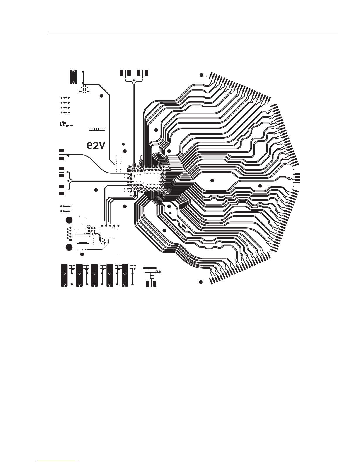
8.2 EV10AS150A-EB Board Layers
Figure 8-8. Top Layer
Appendix
GND
DIODE
ADC
RS
DRTYPE
BI
ST
CLKTYPE
CLKDACTR L
1
EVAL BOARD
ADC EV10AS15xseries
DRR
VINN
GND
VIN
SLEEP
STAGG
3
GND
3V
(3V3)
GND
VCCA3
GND
CLK
SCLK
RESET
DGND
A
DN
SL
SDAT
5
(5.2V)
GND
VCCA
FC
9001281B
GND
GND
(3V3)
VCCD
CLKN
D
V+
(2V5)
DOR/DRDN
9
D
D0
COR/DRCN
C9
C0
DRN
DR
BO
R/DR
BN
B9
B0
A
O
R
/DRA
N
A9
A
0
EV10AS150A-EB User Guide 8-9
e2v semiconductors SAS 2009
ASYNCRST
0977B–BDC–10/09
Page 48
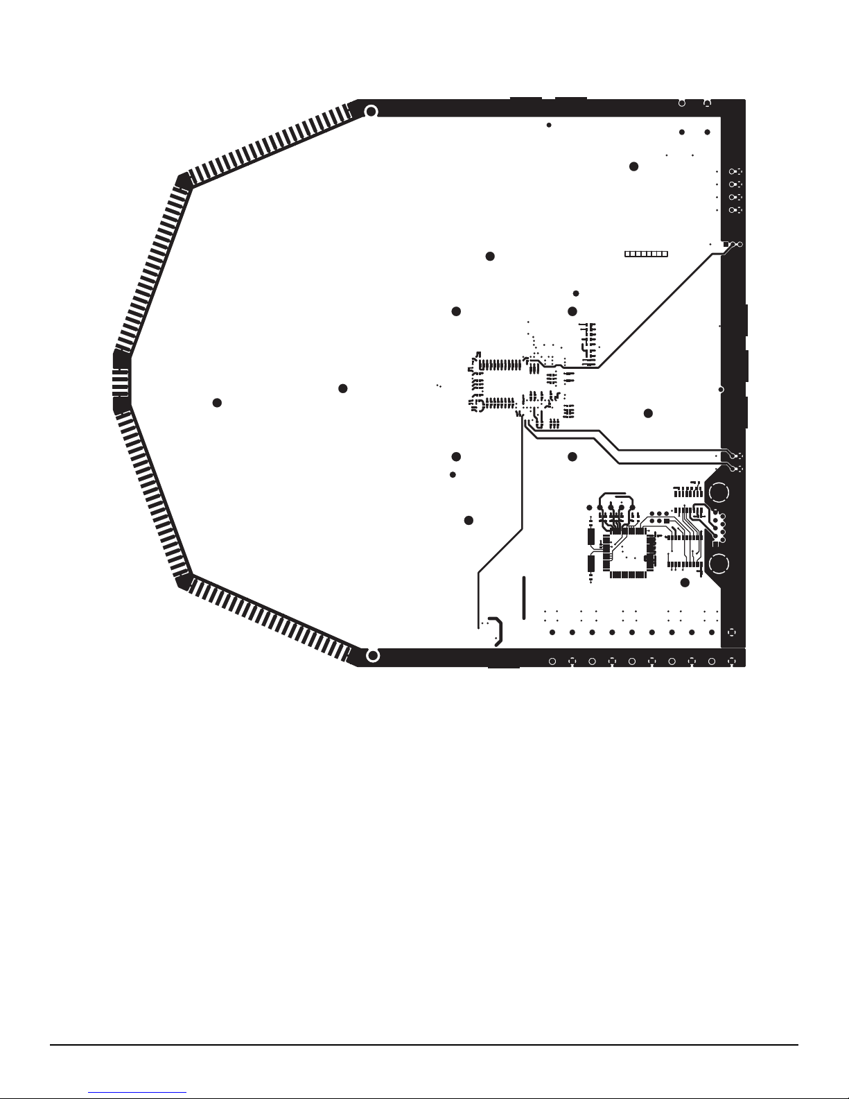
Appendix
Figure 8-9. Bottom Layer
8
8-10 EV10AS150A-EB User Guide
0977B–BDC–10/09
e2v semiconductors SAS 2009
Page 49
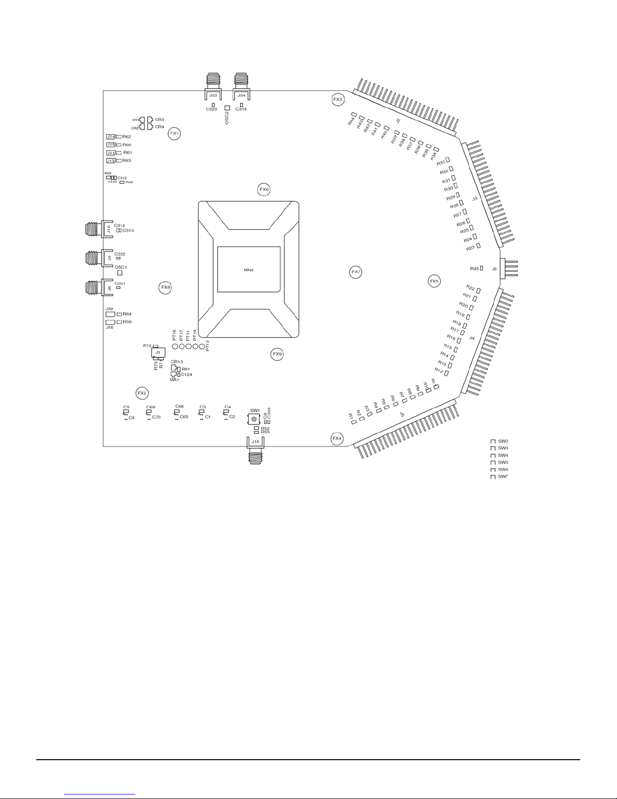
Figure 8-10. Board Equipped with Socket (Top)
Appendix
EV10AS150A-EB User Guide 8-11
e2v semiconductors SAS 2009
0977B–BDC–10/09
Page 50
Appendix
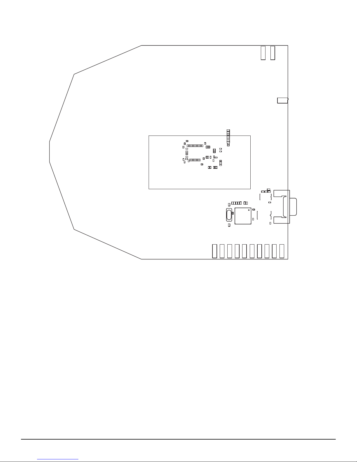
Figure 8-11. Equipped Board (Bottom)
R69
R51
R50
C119
C117
C118
C71
C150
C141
C39
C132
C78
C15
C93
C115
C101
C100
C139
C140
C149
C120
C92
C77
C148
C114
C91
C81
C102
C90
C147
C80
C76
C146
C99
C108
C260
C97
C203
C79
C94
C95
C134
C96
C136
C133
C98
C137
C142
C135
C106
C72
C75
C105
C73
C116
C143
C210
C29
C275
C268
C259
C122
C258
C82
C111
C74
C104
C84
C83
C113
C109
C103
C151
C269
C270
C87
C261
C88
C89
C86
C153
C154
C138
C152
C145
C144
C107
C253
C277
C276
R47
R46
R58
R70
C317
C262
C318
C255
C272
C274
C195
C211
C273
C271
C257
C254
C263
C213
C197
C200C199
C212
C218
C201
C217
C202
C216
C219
C196
C214
C215
C267
C204
C198
C256
All 100 pF caps are welded on 10 nF caps
R82
R80
R75
C127
Y2
C112
C126
R79
MN 2
J21
J22
R53
C68
C62
C64
C60
MN 3
R86
R76
R87
C121
C123
J17
MN 4
C110
C61
J41
J20
J42
J45
J26
J23
J27
J32
J30
J49
8-12 EV10AS150A-EB User Guide
0977B–BDC–10/09
e2v semiconductors SAS 2009
Page 51

How to reach us
Home page: www.e2v.com
Sales offices:
Europe Regional sales office
e2v ltd
106 Waterhouse Lane
Chelmsford Essex CM1 2QU
England
Tel: +44 (0)1245 493493
Fax: +44 (0)1245 492492
mailto: [email protected]
e2v sas
16 Burospace
F-91572 Bièvres Cedex
France
Tel: +33 (0) 16019 5500
Fax: +33 (0) 16019 5529
mailto: [email protected]
e2v gmbh
Industriestraße 29
82194 Gröbenzell
Germany
Tel: +49 (0) 8142 41057-0
Fax: +49 (0) 8142 284547
mailto: [email protected]
Americas
e2v inc
520 White Plains Road
Suite 450 Tarrytown, NY 10591
USA
Tel: +1 (914) 592 6050 or 1-800-342-5338,
Fax: +1 (914) 592-5148
mailto: [email protected]
Asia Pacific
e2v ltd
11/F.,
Onfem Tower,
29 Wyndham Street,
Central, Hong Kong
Tel: +852 3679 364 8/9
Fax: +852 3583 1084
mailto: [email protected]
Product Contact:
e2v
Avenue de Rochepleine
BP 123 - 38521 Saint-Egrève Cedex
France
Tel: +33 (0)4 76 58 30 00
Hotline:
mailto: [email protected]
Whilst e2v has taken care to ensure the accuracy of the information contained herein it accepts no responsibility for the consequences of any use thereof
and also reserves the right to change the specification of goods without notice. e2v accepts no liability beyond that set out in its standard conditions of sale
in respect of infringement of third party patents arising from the use of tubes or other devices in accordance with information contained herein.
e2v semiconductors SAS 2009
0977B–BDC–10/09
 Loading...