


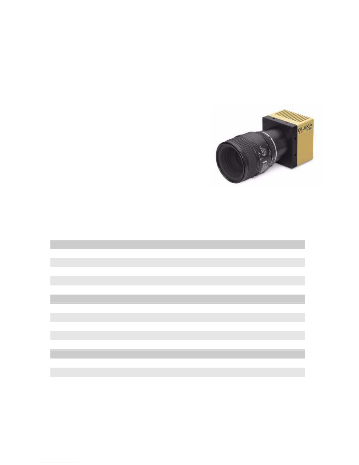
ELiiXA® UC8/UC4
Color Line Scan Camera
1
Eliixa_Color–revF 04/11
e2v semiconductors SAS 2011
ELIIXA UC8/UC4 Camera
User Manual

ELiiXA® UC8/UC4
Color Line Scan Camera
2
Eliixa_Color–revF 04/11
e2v semiconductors SAS 2011
Summary
1 CAMERA OVERVIEW............................................................................4
1.1 Features....................................................................................................................................................4
1.2 Key Specifications.................................................................................................................................. 4
1.3 Description............................................................................................................................................... 5
1.4 Typical Applications ............................................................................................................................... 5
1.5 Models & Part Numbers ........................................................................................................................6
2 CAMERA PERFORMANCES ......................................................................7
2.1 Camera Characterization ...................................................................................................................... 7
2.2 Image Sensor...........................................................................................................................................7
2.2.1 Raw response of the sensor................................................................................................................................................ 8
2.2.2 Response with BG38 filter (for RGB and RGB+B&W versions).................................................................................. 8
2.2.3 Response N-BK7 Band-cut Filter for RGB + Nir version............................................................................................. 9
3 CAMERA HARDWARE INTERFACE........................................................... 10
3.1 Mechanical Drawings............................................................................................................................10
3.2 Input/output Connectors and LED ................................................................................................... 11
3.2.1 Status LED Behaviour .........................................................................................................................................................11
3.2.2 Power Connector ................................................................................................................................................................... 11
3.2.3 Camera Link Output Configuration...................................................................................................................................12
4 STANDARD CONFORMITY ................................................................... 14
4.1 CE Conformity........................................................................................................................................14
4.2 FCC Conformity .....................................................................................................................................14
4.3 RoHs Conformity................................................................................................................................... 14
5 SETTING UP THE CAMERA IN THE SYSTEM.............................................. 15
6 CAMERA SOFTWARE INTERFACE........................................................... 16
6.1 Control and Interface ......................................................................................................................... 16
6.2 Serial Protocol and Command Format..............................................................................................17
6.2.1 Syntax .....................................................................................................................................................................................17
6.2.2 Command Processing ............................................................................................................................................................17
6.3 Camera Commands ................................................................................................................................18
6.3.1 Information, Status and Communication ........................................................................................................................19
6.3.2 Output modes and Spatial Rebuild ..................................................................................................................................23
6.3.3 Exposure and Synchronization.........................................................................................................................................28
6.3.4 Gain and Offset ...................................................................................................................................................................33
6.3.5 Color Management ...............................................................................................................................................................39
6.3.6 Flat Field Correction ..........................................................................................................................................................46

ELiiXA® UC8/UC4
Color Line Scan Camera
3
Eliixa_Color–revF 04/11
e2v semiconductors SAS 2011
6.3.7 Save & Restore Settings ...................................................................................................................................................54
7 APPENDIX A: Camera Status Details........................................................ 55
7.1 Table 1 : Processing Status .......................................................................................................................55
7.2 Table 2 : Internal Task Status ........................................ ... .................................. ...................................... 55
7.3 Table 3 : Error Diagnostic Status........................................................................ ... ...................................56
8 APPENDIX C : Thermal Management ........................................................ 57
9 APPENDIX E: Optical Mounts available ...................................................... 58
APPENDIX F: Color Matrix Examples ............................................................ 59
APPENDIX F: Color Matrix Examples ............................................................ 60
10 APPENDIX G: Revision History ............................................................ 61
ELiiXA® UC8/UC4
4
Eliixa_Color–revF 04/11
e2v semiconductors SAS 2011
1 CAMERA OVERVIEW
1.1 Features
• Sensor: 3 or 4 x 4096 pixels 10 x 10 µm
• Multi-line with 3 Versions (each of them in Full or Low speed):
–
RGB
–
RGB
+ Monochrome
–
RGB
+ Near Infra Red
• Rows Spacing of Tw o Pixels (Centre to Centre)
• Boosted Blue Response
• Line Rate Up to 18 KHz
• Camera Link® Interface (Dual Base, Medium)
• Mechanics: 70 x 76 x 54 mm3
• Automated White Balance and Flat Field Correction
• Bidirectional Scanning
• Tun ea ble Spatial Correction
• Internal 4x4 Color Matrix Correction
1.2 Key Specifications
Sensor Characteristics at Maximum Pixel Rate
Resolution
Pixels 3 or 4 x 4096
Pixel Size (square) µm 10 x 10
Spacing between rows µm 20 (center to center)
Line Length mm 40,96
Max Line Rate kHz 18 (Full Speed Version) or 13 (low speed Version.)
Radiometric Performance at Maximum Pixel Rate
Bit Depth Bits 8, 10 or 12
Responsivity LSB/(nJ/cm²) 136
Response Non linearity
% ±1
PRNU (not corrected) % < 10
Dynamic Range dB 62
Functionalities (Programmable via Control Interface)
Gain Up to 25.4 dB
Offset -4096 to +4096 LSB
Tri g g er M ode Timed (Free run) and triggered (Ext Trig, Ext ITC) modes

ELiiXA® UC8/UC4
5
Eliixa_Color–revF 04/11
e2v semiconductors SAS 2011
Mechanical and Electrical Interface
Size (w x h x l) mm 70 x 76 x 54
Weight g 470 (without mount)
Lens Mount
F, T2, M42 x 1 compliant with AVIIVA SM2 series
Sensor Alignment µm ±100
Sensor flatness µm ±35
Power Supply V Single 12 to 24
Power Dissipation W < 15
Current Consumption A Max 2A at the startup
General features
Operating Temperature °C 0 to 65 (front face)
Storage Temperature °C -40 to 70
Regulatory CE, FCC and RoHS compliant
1.3 Description
The ELiiXA
Color
camera is the ideal candidate for the most demanding applications requiring multi
wavelength detection
(including NIR). Using e2v’s unique technology, the CCD sensor features unmatched
performance: line rate up to
18
KHz, row spacing of two pixels center to center, enhanced blue response,
three lines (RGB) and four lines (RGB and fourth line either monochrome or NIR). The camera package is
designed to increase efficiency and save cost at vision sys
tem
level:
• Easy calibration (Automatic Tap balance and flat field correction, white balance, Color correction)
• versatile implementation (trigger modes, output modes, bidirectional scanning, spatial correction)
and
with an all-in-one approach, a single ELiiXA camera can replace a two camera system of a conventional
color camera and a monochrome or NIR camera.
The Fourth monochrome line will give you more accuracy to define colors in CIE color system and the NIR
version will help you to see even what the eyes can’t see.
1.4 Typical Applications
• Web Inspection: Printing, Currency
• High-end Inspection: Food, Pharmaceutical, Medical, Packaging
• Surface Inspection: Ceramic tiles, Wood, Printed Circuit Board
• Scanning: High-end Document Process, Film scanning, Postal sorting
• Metrology : Color matching

ELiiXA® UC8/UC4
6
Eliixa_Color–revF 04/11
e2v semiconductors SAS 2011
1.5 Models & Part Numbers
Part Number Sensor Speed Additional Filter included
EV71YUC8CL4010-BA0 RGB Full Speed : 18 KHz BG38 2mm IR cut-off
EV71YUC8CL4010-BA1 RGB + B&W Full Speed : 18 KHz BG38 2mm IR cut-off
EV71YUC8CL4010-BA2 RGB + NIR Full Speed : 18 KHz Band-cut Filter on N-BK7 Glass
EV71YUC4CL4010-BA0 RGB Low Speed : 13 KHz BG38 2mm IR cut-off
EV71YUC4CL4010-BA1 RGB + B&W Low Speed : 13 KHz BG38 2mm IR cut-off
EV71YUC4CL4010-BA2 RGB + NIR Low Speed : 13 KHz Band-cut Filter on N-BK7 Glass
ELiiXA® UC8/UC4
7
Eliixa_Color–revF 04/11
e2v semiconductors SAS 2011
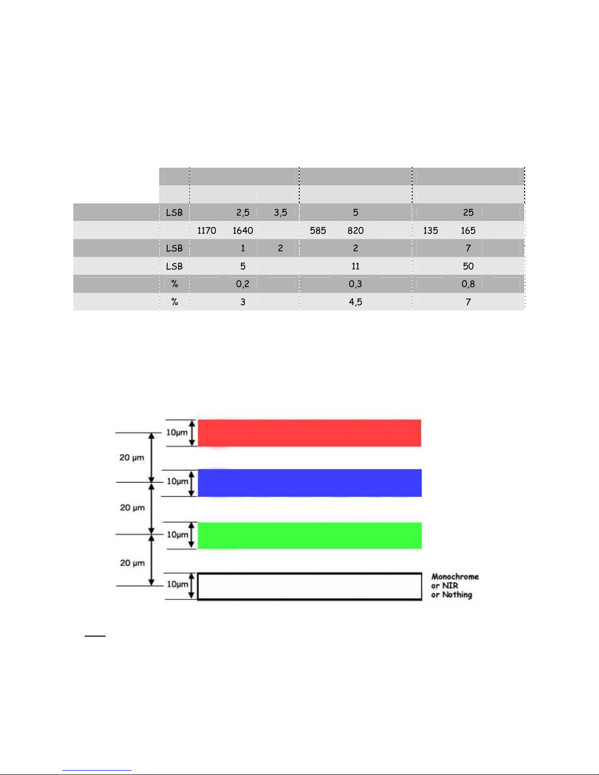
2 CAMERA PERFORMANCES
2.1 Camera Characterization
Unit Min Gain Min Gain +10dB Min Gain +20dB
Min Typ. Max Min Typ. Max Min Typ. Max
Dark Noise RMS LSB 2,5 3,5 5 25
Dynamic Range 1170 1640 585 820 135 165
FPN rms LSB 1 2 2 7
FPN pk pk LSB 5 11 50
PRNU rms % 0,2 0,3 0,8
PRNU pk pk % 3 4,5 7
Note : These figures in LSB are for a 12bits format.
2.2 Image Sensor
Note: The real order of the color line is Red–Blue–Green but the Camera outputs in Red–Green–Blue order on
the Camera Link connector.

ELiiXA® UC8/UC4
8
Eliixa_Color–revF 04/11
e2v semiconductors SAS 2011
2.2.1 Raw response of the sensor
.
2.2.2 Response with BG38 filter (for RGB and RGB+B&W versions)

ELiiXA® UC8/UC4
9
Eliixa_Color–revF 04/11
e2v semiconductors SAS 2011
2.2.3 Response N-BK7 Band-cut Filter for RGB + Nir version
The sensor has been designed to give in the Near Infra Red (800-1100nm) an equal answer of each Red, Green
and Blue colors than the Nir line itself.
In order to remove simply the Near Infra Red component from each Red, Green and Blue colors, we can define
the following Color Correction Matrix:
( R’ B’ G’ Nir’) = 1 0 0 -1 R
0 1 0 -1 B
0 0 1 -1 G
0 0 0 1 Nir
Depending on your light source, some other combination of filter can be provided.
For more information, please, contact the Hotline Camera : hotline-cam@e2v.com

ELiiXA® UC8/UC4
10
Eliixa_Color–revF 04/11
e2v semiconductors SAS 2011
3 CAMERA HARDWARE INTERFACE
3.1 Mechanical Drawings
Sensor alignment
Z = 10,9mm ±150µm
X = 14,52mm ±100 µm
Y = 38mm ±100 µm
Planarity ±35 µm
Rotation (X,Y plan) ±0,2°
Tilt (versus lens mounting plane)
±35µm
References :
First Pixel
Optical axe as (X,Y) reference
Front face as Reference Face

ELiiXA® UC8/UC4
11
Eliixa_Color–revF 04/11
e2v semiconductors SAS 2011
3.2 Input/output Connectors and LED
3.2.1 Status LED Behaviour
After less than 2 seconds of power establishment, the LED first lights up in RED. Then after a Maximum of 8
seconds, the LED must turn in one of the following colors:
Color and state Meaning
Green
and continuous
OK
Green
and blinking slowly
Waiting for Ext Trig (Trig1 and/or Trig2)
Red
and continuous
Camera out of order : Internal firmware error
3.2.2 Power Connector
Camera connector type: Hirose HR10A-7R-6PB (male)
Cable connector type: Hirose HR10A-7P-6S (female)
Signal Pin Signal Pin
PWR 1 GND 4
PWR 2 GND 5
PWR 3 GND 6
Camera side description
Power supply from 12v to 24v
Power 15W max with an inrush current of 2A
during power up
Double CameraLink
Connectors for all
possible modes :
Medium / Dual Base
Power Connector :
Hirose 6pts
12v to 24v
Multi-colored LED
for status
And diagnostic

ELiiXA® UC8/UC4
12
Eliixa_Color–revF 04/11
e2v semiconductors SAS 2011
3.2.3 Camera Link Output Configuration
Notes
:
1) On RGB Models only one mode : RGB 8bits 3x80 or 3x60MHz. The Connector CL2 is not used.
2) On RGB models, the medium 8 bits is equivalent to a base 8 bits because there is no fourth channel.
Connector CL1 assignment table:
Port/Bit
Dual Base
3x8 + 1x8bits
Dual Base
3x8 + 1x10bits
Dual Base
3x8 + 1x12bits
Dual Base
3x8 + 3x8bits
Medium
10 bits
Medium
12 bits
Dual Base
Interlaced
RGB
Port A0 R0 R0 R0 R0 R0 R0 R0
Port A1 R1 R1 R1 R1 R1 R1 R1
Port A2 R2 R2 R2 R2 R2 R2 R2
Port A3 R3 R3 R3 R3 R3 R3 R3
Port A4 R4 R4 R4 R4 R4 R4 R4
Port A5 R5 R5 R5 R5 R5 R5 R5
Port A6 R6 R6 R6 R6 R6 R6 R6
Port A7 R7 R7 R7 R7 R7 R7 R7
Port B0 G0 G0 G0 G0 R8 R8 G0
Port B1 G1 G1 G1 G1 R9 R9 G1
Port B2 G2 G2 G2 G2 nc R10 G2
Port B3 G3 G3 G3 G3 nc R11 G3
Port B4 G4 G4 G4 G4 B8 B8 G4
Port B5 G5 G5 G5 G5 B9 B9 G5
Port B6 G6 G6 G6 G6 nc B10 G6
Port B7 G7 G7 G7 G7 nc B11 G7
Port C0 B0 B0 B0 B0 B0 B0 B0
Port C1 B1 B1 B1 B1 B1 B1 B1
Port C2 B2 B2 B2 B2 B2 B2 B2
Port C3 B3 B3 B3 B3 B3 B3 B3
Port C4 B4 B4 B4 B4 B4 B4 B4
Port C5 B5 B5 B5 B5 B5 B5 B5
Port C6 B6 B6 B6 B6 B6 B6 B6
Port C7 B7 B7 B7 B7 B7 B7 B7
Modes Connector CL1 Connector CL2
Notes
Dual Base 3 + 1
RGB
8bits + Nir/Mono 8bits
RGB
: 3x80 or 3x60MHz
Nir or Mono 1x80 or 1x60MHz
1
RGB
8bits + Nir/Mono 10bits
RGB
: 3x80 or 3x60MHz
Nir or Mono 1x80 or 1x60MHz
1
RGB
8bits + Nir/Mono 12bits
RGB
: 3x80 or 3x60MHz
Nir or Mono 1x80 or 1x60MHz
1
Dual Base 3 + 3
RGB
8bits + RGNir/RGMono 8bits
RGB
: 3x80 or 3x60MHz
RG
Nir/RGMono 3x80 or 3x60MHz
1
RGB
8bits + RBNir/RBMono 8bits
RGB
: 3x80 or 3x60MHz
RB
Nir/RBMono 3x80 or 3x60MHz
1
RGB
8bits + GBNir/GBMono 8bits
RGB
: 3x80 or 3x60MHz
GB
Nir/GBMono 3x80 or 3x60MHz
1
Medium
RBG
Nir /
RBG
Mono 8bits
RGB
: 3x80 or 3x60MHz
Nir or Mono 1x80 or 1x60MHz
2
RBG
Nir /
RBG
Mono 10bits
Camera Link Standard Medium mode in 4x80 or 4x60MHz
2
RBG
Nir /
RBG
Mono 12bits
Camera Link Standard Medium mode in 4x80 or 4x60MHz
2
Dual Base Interlaced 8bits (RGB -BA0- Camera Only)
RBG
odd +
RBG
even 8bits
RGB
odd: 3x40 or 3x30MHz
RGB
even: 3x40 or 3x30MHz
3

ELiiXA® UC8/UC4
13
Eliixa_Color–revF 04/11
e2v semiconductors SAS 2011
Connector CL2 assignment table:
Port/Bit
Dual Base
3x8 + 1x8bits
Dual Base
3x8 + 1x10bits
Dual Base
3x8 + 1x12bits
Dual Base
3x8 + 3x8bits
Medium
10 bits
Medium
12 bits
Dual Base
Interlaced
RGB
Port D0 M0 M0 M0 R0 M0 M0 R0
Port D1 M1 M1 M1 R1 M1 M1 R1
Port D2 M2 M2 M2 R2 M2 M2 R2
Port D3 M3 M3 M3 R3 M3 M3 R3
Port D4 M4 M4 M4 R4 M4 M4 R4
Port D5 M5 M5 M5 R5 M5 M5 R5
Port D6 M6 M6 M6 R6 M6 M6 R6
Port D7 M7 M7 M7 R7 M7 M7 R7
Port E0 nc M8 M8 G0 G0 G0 G0
Port E1 nc M9 M9 G1 G1 G1 G1
Port E2 nc nc M10 G2 G2 G2 G2
Port E3 nc nc M11 G3 G3 G3 G3
Port E4 nc nc nc G4 G4 G4 G4
Port E5 nc nc nc G5 G5 G5 G5
Port E6 nc nc nc G6 G6 G6 G6
Port E7 nc nc nc G7 G7 G7 G7
Port F0 nc nc nc M0 G8 G8 B0
Port F1 nc nc nc M1 G9 G9 B1
Port F2 nc nc nc M2 nc G10 B2
Port F3 nc nc nc M3 nc G11 B3
Port F4 nc nc nc M4 M8 M8 B4
Port F5 nc nc nc M5 M9 M9 B5
Port F6 nc nc nc M6 nc M10 B6
Port F7 nc nc nc M7 nc M11 B7
Port G0 nc nc
nc nc nc nc nc
Port G1 nc nc nc nc nc nc nc
Port G2 nc nc nc nc
nc nc nc
Port G3 nc nc nc nc nc nc nc
Port G4 nc nc nc nc
nc nc nc
Port G5 nc nc nc nc nc nc nc
Port G6 nc nc nc nc
nc nc nc
Port G7 nc nc nc nc nc nc nc
Port H0 nc nc nc nc
nc nc nc
Port H1 nc nc nc nc nc nc nc
Port H2 nc nc nc nc nc nc nc
Port H3 nc nc nc nc nc nc nc
Port H4 nc nc nc nc nc nc nc
Port H5 nc nc nc nc nc nc nc
Port H6 nc nc nc nc
nc nc nc
Port H7 nc nc nc nc nc nc nc
Rx, Gx, Bx = Bit x, for color Red, Green or Blue.
Mx = Bit x for Monochrome or Nir

ELiiXA® UC8/UC4
14
Eliixa_Color–revF 04/11
e2v semiconductors SAS 2011
4 STANDARD CONFORMITY
The ELIIXA cameras have been tested using the following equipment:
• A shielded power supply cable
• A Camera Link data transfer cable ref. 14B26-SZLB-500-OLC (3M)
e2v recommends using the same configuration to ensure the compliance with the following standards.
4.1 CE Conformity
The ELIIXA cameras comply with the requirements of the EMC (European) directive 89/336/CEE (EN
50081-2, EN 61000-6-2).
4.2 FCC Conformity
The ELIIXA cameras further comply with Part 15 of the FCC rules, which states that:
Operation is subject to the following two conditions:
• This device may not cause harmful interference, and
• This device must accept any interference received, including interference that may cause undesired
operation.
This equipment has been tested and found to comply with the limits for Class A digital device, pursuant
to part 15 of the FCC rules. These limits are designed to provide reasonable protection against harmful
interference when the equipment is operated in a commercial environment. This equipment generates,
uses and can radiate radio frequency energy and, if not installed and used in accordance with the
instruction manual, may cause harmful interference to radio communications. Operation of this equipment
in a residential area is likely to cause harmful interference in which case the user will be required to
correct the interference at his own expense.
4.3 RoHs Conformity
ELIIXA cameras comply with the requirements of the RoHS directive
Warning
: Changes or modifications to this unit not expressly approved by the party responsible
for compliance could void the user's authority to operate this equipment.

ELiiXA® UC8/UC4
15
Eliixa_Color–revF 04/11
e2v semiconductors SAS 2011
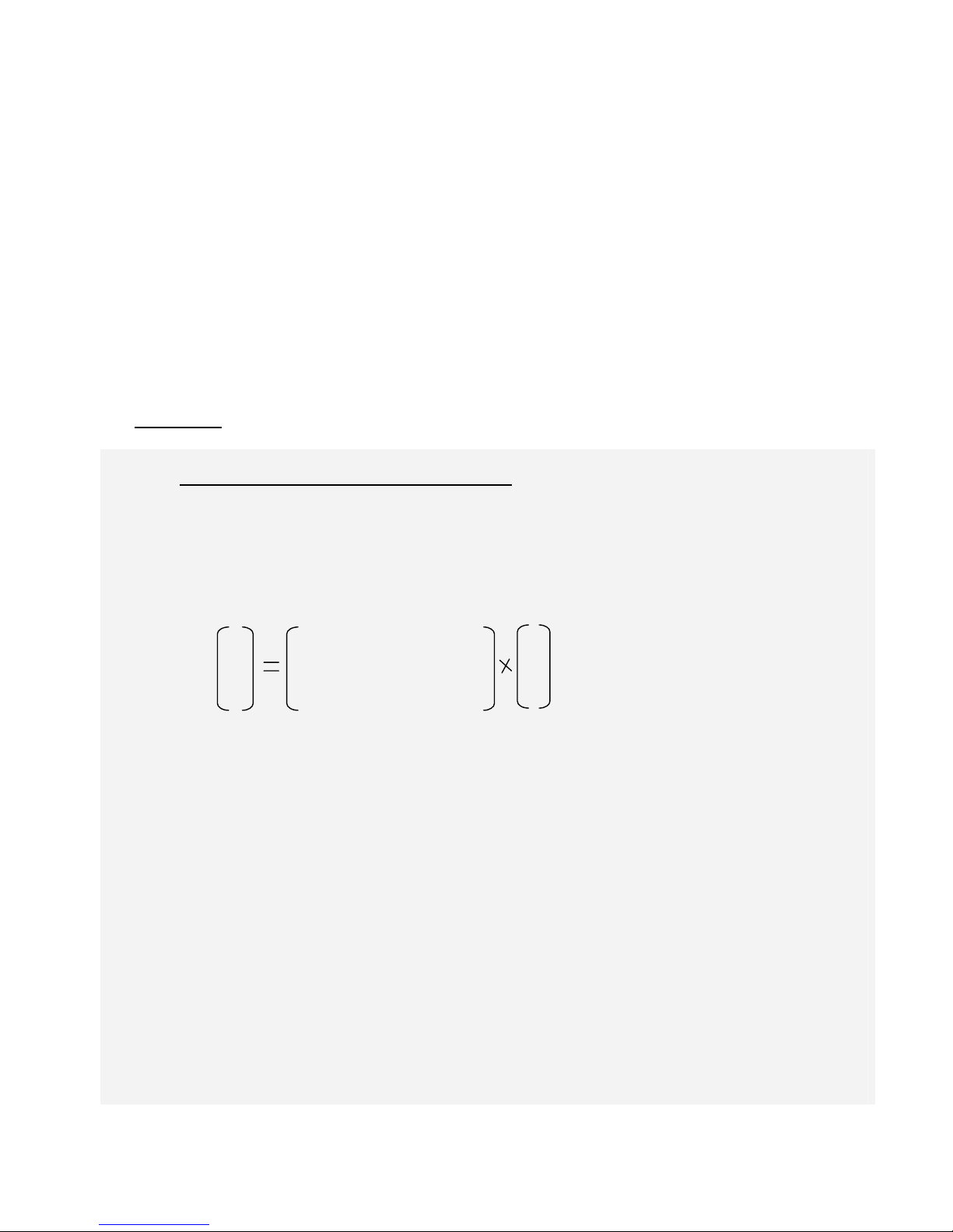
5 SETTING UP THE CAMERA IN THE SYSTEM
Vocabulary:
w
= size of the sensor line (40,96mm)
FOV
= Field Of View (width of the web inspected by the sensor line) in mm.
L
= Working distance (from the Lens to the Web) in mm.
f
= focal distance of the lens in mm.
S
= Speed of the web in mm/s
We have:
w/FOV = f/L
The ratio M = w/FOV is called Magnification.
The FOV is grabbed by 4096 pixels in the width.
In order to get a ratio of 1 :1 in your image, at the web speed of S, your line rate has to be set:
Line Rate = (S/FOV) x 4096
Ex
: if the FOV = 11 cm (110mm) and the speed of the web is S= 0,3 m/s (300mm/s) the line rate will be:
Line Rate = (300 /110) x 4096 = 11170 Lines/s.
The spatial correction has to be set to 2 because the spacing between two color lines in the sensor is
20µm center to center (2 lines of 10µm width).
If you use a 60mm lens, the working distance will be: L = (60 x 110) 40,96 = 161mm.
This will certainly require a macro lens.

ELiiXA® UC8/UC4
16
Eliixa_Color–revF 04/11
e2v semiconductors SAS 2011
6 CAMERA SOFTWARE INTERFACE
6.1 Control and Interface
As all the e2v Cameras, the ELIIXA is delivered with the friendly interface control software COMMCAM.UCL
(as “Ultimate Camera Link”) which is based on the GenICam standard
COMMCAM recognizes and detects automatically all the UCL Cameras connected on any transport layers
(Camera Link or COM ports) of your system.
Once connected to the Camera you have an easy access to all its fe atures. The visibility of these features can
be associated to three types of users: Beginner, Expert or Guru. Then you can make life easy for simple users.

ELiiXA® UC8/UC4
17
Eliixa_Color–revF 04/11
e2v semiconductors SAS 2011
6.2 Serial Protocol and Command Format
The Camera Link interface provides two LVDS signal pairs for communication between the camera and
the frame grabber. This is an asynchronous serial communication based on RS-232 protocol.
The serial line configuration is:
• Full duplex/without handshaking
• 9600 bauds (default), 8-bit data, no parity bit, 1 stop bit. The baud rate can be set up to 230,400
6.2.1 Syntax
Internal camera configurations are activated by write or readout commands.
The command syntax for write operation is:
w <command_name> <command_parameters><CR>
The command syntax for readout operation is:
r <command_name><CR>
6.2.2 Command Processing
Each command received by the camera is processed:
• The setting is implemented (if valid)
• The camera returns “>”<return code><CR>
We recommend to wait for the camera return code before sending a new command.
Table 5-1. Camera Returned Code
Returned code meaning
>0
(or “>OK”) : All right, the command will be implemented
>3
Error bad CRC in command
>16
Command Error (Command not recognize or doesn't exist)
>21
Invalid Command ID (the Command doesn't exist).
>33
Invalid Access (the receipt of the last command has failed).
>34
Parameter out of range (the parameter of the last command send is out of range).
>35
Access Failure (bad communication between two internal devices).

ELiiXA® UC8/UC4
18
Eliixa_Color–revF 04/11
e2v semiconductors SAS 2011
6.3 Camera Commands
Information, statu
s
and Communicatio
n
- Vendor Name / Model Name
- Camera ID / Customer ID
- Status
- Software version
- Dump
- Baud Rate
Output modes and spatial rebuild
- Signal Source
- Output Mode
- Scanning Direction
- Spatial Correction
Exposure and Synchronizatio
n
- Synchronization Modes
- Integration Time
- Line Period
Gain and Offse
t
- Preamp Gain
- Gain
- Digital Gain & Offset
- Tap Balance Management
Colo
r
Managemen
t
- White Balance Gains setting
- Auto White Balance Management
- Color Matrix Management & setting
Flat Field Correctio
n
- FFC Management
- PRNU / DSNU reset
- PRNU / DSNU Manual setting
- FFC Save & Restore
Save & Restore Setting
s
- Factory setting restore
- User settings Save & Restore

ELiiXA® UC8/UC4
19
Eliixa_Color–revF 04/11
e2v semiconductors SAS 2011
6.3.1 Information, Status and Communication
• Information : These values allow to identify the Camera. They can be accessed through the CommCam
software in the “Info” section
All these values are fixed in factory except the Camera User ID which can be fixed by the Customer:
o Vendor name
: “e2v”
Read function: “r vdnm”;
Return by the camera: “e2v” (string)
Can not be written
o Model Name
: Internal name for GenICam :
=> Read function: “r mdnm”;
return by the camera (string) :
EliixaUC8CL_RGB_NI_v1
EliixaUC4CL_RGB_NI_v1
EliixaUC8CL_RGB_BW_v1
EliixaUC4CL_RGB_BW_v1
EliixaUC8CL_RGB_v1
EliixaUC4CL_RGB_v1
=> Can not be written
o Camera ID
: part number, serial number of the Camera
=> Read function : “r idnb”;
Return by the camera (string 50 bytes max) :
ex : EV71YUC8CL4010-BA2-0000000000-0806P2009-1A
with :
EV71YUC8CL4010-BA2 : Part number
0000000000 : Batch number (not used for Cameras)
0806P2009 : Serial number
• “08” : Year of manufacturing
• “06” : week in the year
• “P” as Proto, “M” as Manual, “A” as automatic : type of testing
• “2009” : Identification number
1A: Fab indice.
=> Can not be written
o User ID
: Can be set by the Customer to identify the Camera
Ö Read function : “r cust”;
Return by the camera (string 50 bytes max) :
Ö Write function : “w cust” <string>;
ELiiXA® UC8/UC4
20
Eliixa_Color–revF 04/11
e2v semiconductors SAS 2011
o Firmware Version : Can be set by the Customer to identify the Camera
Ö Read function : “r vers”;
Return <id+ver #0>-<id+ver #1>
With <id+ver #N> = hexadecimal 32-bits long for id and version for module N
The format of a 32-bits value is:
Bit 0 to 3 : 0
Bit 4 to 7 : module number
Bit 8 to 19 : module identifier
Bit 20 to 25 : major version
Bit 26 to 31 : minor version
Ex :
0C100230 translated into binary :
0000 1100 0001 0000 0000 0010 0011 0000
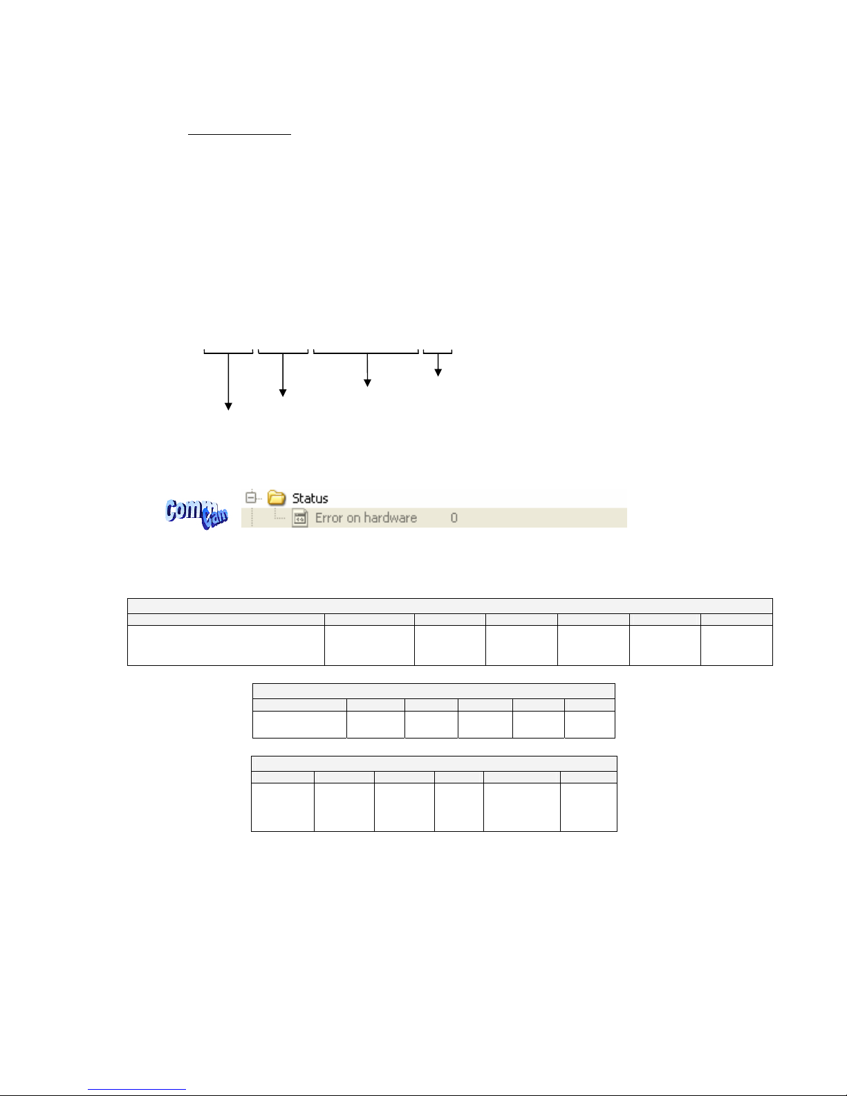
• Status : Give the Camera Status. It can be accessed in CommCam software in the “Status” section :
Ö Read function : “r stat”;
Return by the camera : A 32 bits integer value composed as follows :
Statut Diagnostique Erreur
31 22 21 20 19 18 17 16
0000 0000 00
Err CommCam
compatibility
index
Err user
camera
settings
Err factory
camera
settings
Err user
application
settings
Err factory
application
settings
Err
hardware
init
internal Task Status
15 13 12 11 10 9 8
000 0
Cal/App
Enabled
Warn
Udf
Warn
Ovf
Processing Status
7 6 5 4 2 1 0
Settings
Modified
Tap
Balance
Modified
FFC
Modified
000
reserved
Wait for
trigger
=> All these Values are explained in the APPENDIX A
Module number
Module identifie
r
Major version
Minor version

ELiiXA® UC8/UC4
21
Eliixa_Color–revF 04/11
e2v semiconductors SAS 2011
•
Dump: Allows to dump all the Camera info/settings in a text file. This command is available in the
CommCam View Menu:
=> Read function : “r dump”;
• BaudRate: Set the Camera BaudRate. This command is available in the CommCam “Com” section :
Ö Read function : “r baud”;
Return by the camera : Value of the Baud Rate
Ö Write function : “w baud” <index> with the index as follows :
1 : 9600 Bauds (default value at power up)
2 : 19200Bds
6 : 57600Bds
12 : 115200Bds
24 : 230400Bds
After changing the communication rate, the communication with the Camera could be interrupted
with the application (CommCam or whatever) it has made this change. The application has to
reconnect. the baudrate will automatically switch to 9600 bds at the next power down/up

ELiiXA® UC8/UC4
22
Eliixa_Color–revF 04/11
e2v semiconductors SAS 2011
Title Command Features
VendorName r vdnm Get camera vendor name
Return string e2v
ModelName r mdnm Get camera model name
Return string
Camera ID r idnb Get camera ID.
Return <idstr> Max 50 bytes
w cust <idstr> Set customer ID to <idstr>.
<idstr> format is : my camera …. Max 50 bytes
User ID
r cust Get customer ID.
Return <idstr>
Firmware version r vers Get the camera software version
Return <id+ver #0>-<id+ver #1>
With <id+ver #N> = hexadecimal 32-bits long for id and version
for module N
Status r stat Get camera status
Dump r dump Get camera configuration with the format:
idnb AT71…
fing 5
fga1 120
w baud 1 Set CL RS232 baudrate to 9600Bds (always boot with
9600bds)
w baud 2 Set CL RS232 baudrate to 19200Bds
w baud 6 Set CL RS232 baudrate to 57600Bds
w baud 12 Set CL RS232 baudrate to 115200Bds
w baud 24 Set CL RS232 baudrate to 230400Bds
Baudrate
r baud Get current baud rate

ELiiXA® UC8/UC4
23
Eliixa_Color–revF 04/11
e2v semiconductors SAS 2011
6.3.2 Output modes and Spatial Rebuild
• Signal source
: Defines if the data comes from the Sensor or the FPGA (test Pattern). This command is
available in the CommCam “Setup” section :
Ö Read function : “r srce”;
Return by the camera: “0” if Source from the Sensor and “1” if test pattern active
Ö Write function : “w srce” <value> :
“0” to switch to CCD sensor image
“1” to switch to Test Pattern.
The Test pattern is a single ramp. The detail of this test pattern is given in
APPENDIX B.
The test pattern is generated in the FPGA : It’s used to point out any interface
problem with the Frame Grabber.
The test pattern is generated by the FPGA. This is a 12bit width pattern identical for each line as following:
R G B Nir
0 80 40 C0
1 81 41 C1
2 82 42 C2
3 83 84 C3
… … … …
… … … …
… … … …
F00 F80 F40 FC0
F01 F81 F41 FC1
… … … …
… … … …
F3F FBF F7F FFF
F40 FC0 F80 FFF
… … … …
… … … …
FFD FFF FFF FFF
FFE FFF FFF FFF
FFF FFF FFF FFF

ELiiXA® UC8/UC4
24
Eliixa_Color–revF 04/11
e2v semiconductors SAS 2011
• Output mode
: Set the Camera Link Output mode (refer to Chap 3.2.3 : Camera Link Output
Configuration). This command is available in the CommCam “Output” section :
Ö Read function : “r mode”;
Return by the camera : Output mode from 0 to 9 (see below).
Ö Write function : “w mode” <value> :
• Scanning direction
: Set the scanning direction of the Camera. This command is available in the
CommCam “Spatial Rebuild” section :
Ö Read function : “r rway”;
Return by the camera :
• 0 : Reverse
• 1 : Forward
Ö Write function : “w rway” <value>
Value Modes
Dual Base 3 + 1
0 RGB
8bits + Nir/Mono 8bits
1 RGB
8bits + Nir/Mono 10bits
2 RGB
8bits + Nir/Mono 12bits
RBG
8bits for 3-Linear versions
Dual Base 3 + 3
7 RGB
8bits + RGNir/RGMono 8bits
8 RGB
8bits + RBNir/RBMono 8bits
9 RGB
8bits + GBNir/GBMono 8bits
RBG
8bits for 3-Linear versions
Medium
3 RBG
Nir /
RBG
Mono 8bits
RBG
8bits for 3-Linear versions
4 RBG
Nir /
RBG
Mono 10bits
RBG
10bits for 3-Linear versions
5 RBG
Nir /
RBG
Mono 12bits
RBG
12bits for 3-Linear versions
Dual Base Interlaced 8bits
RGB (BA0) versions only
13 RGB
8bits odd +
RGB
8bits even
2 connectors interlaced odd/even

ELiiXA® UC8/UC4
25
Eliixa_Color–revF 04/11
e2v semiconductors SAS 2011
Definition of Forward / Reverse
:
• Spatial Correction
: Set the number of lines (0 up to 6) for the spatial correction (see explanation
below). This command is available in the CommCam “Spatial Rebuild” section :
Ö Read function : “r loop”;
Return by the camera : 0 to 8 :
0 : Correction inhibited
1 : Delay 0,5 lines
2 : Delay 1 line
3 : Delay 1,5 lines
4 : Delay 2 lines
5 : Delay 3 lines
6 : Delay 4 lines
7 : Delay 5 lines
8 : Delay 6 lines
Ö Write function : “w loop” <value>
Forward
Direction
(Web)
2
3
…
Pixel numbers

ELiiXA® UC8/UC4
26
Eliixa_Color–revF 04/11
e2v semiconductors SAS 2011
The spatial correction has changed since the firmware version 3.0.0
On all previous versions, only the delays from 1 to 7 were available with the associated loop value.
For more information, please contact the Hotline : hotline-cam@e2v.com
What is the Spatial correction ?
Vocabulary
:
w= Pixel Size : 10µm in the Eliixa
W = Size of the real object of the web seen by one pixel
M = Magnification : M = w/W
p = Color pitch or distance between to lines centers = 20µm in the
Eliixa
S = Speed of the web.
For magnification of M, the line rate has to be adjusted at S/W
(see Chapter 5). Then, due to the fact that the color pitch is 2x the
pixel size, an area size of W which has been grabbed by the red line
at T will be grabbed by the Blue at T+2, by the Green at T+4 …
The Camera memorizes each line for each color from T to T+6.
The spatial correction of “2” allows to associate :
Red (T) + Blue(T+2) + Green (T+4) + Nir/BW(T+6) to be outputted in
the same time on the Camera Link connector.
Then the Spatial correction of “2” is for a pixel ratio (width/height) of 1/1 (“square pixels”).
We define the “width” in the sensor direction and the “height” in the web direction : A web speed which is 2x
times faster than the appropriate line rate to get square pixels will compress by 2 the pixels in the web
direction : In this case the ratio will be defined as 1/2.
But if the ratio is different, in order to avoid color artifacts, you’ve to adjust your spatial correction in the
following range :
Delay Ratio
Inhibited 0,5 1/4
1 1/2
1,5 2/3
2 1/1
3 3/2
4 2/1
5 5/2
6 3/1
T+6 T+5 T+4 T+3 T+2 T+1 T
Web Direction
Sensor
Lens
Example :
Sensor size = 40,96mm
(pixel size = 10µm)
Web Speed = 2200mm/s
Web Width = 500mm
Focal length = 65mm
Magnification = 0,08192 :
(sensor size/ Web width)
=> 10µ on the sensor Ù 0,12207mm on the Web
At 18000l/s, the actual web speed (2200mm/s) is covered : The
spatial correction has to bet set to 2, the image ratio will be 1/1
Working distance => 793,5mm :
(Focal length / Magnification)
If the Web speed is set at 4400mm/s, the image ratio will be 1/2 and
then the Spatial correction has to be set to 1 (line rates remains
18000l/s for the Camera : It’s the max it can achieve.

ELiiXA® UC8/UC4
27
Eliixa_Color–revF 04/11
e2v semiconductors SAS 2011
Title Command Features
w srce 0 Set signal source to CCD sensor
w srce 1 Set signal source to user pattern
Signal Source
r srce Get current signal source
w mode 0 set 3+1 outputs Dual Base 8/ 8bits (*)
w mode 1 3+1 outputs Dual Base 8/10bits (*)
w mode 2 3+1 outputs Dual Base 8/12bits (*)
w mode 3 4 outputs Medium 8bits
w mode 4 4 outputs Medium 10bits
w mode 5 4 outputs Medium 12bits
w mode 7 3+3 outputs dual base 8 bits RGB + RGNir/RGMono (*)
w mode 8 3+3 outputs dual base 8 bits RGB + RBNir/RBMono (*)
w mode 9 3+3 outputs dual base 8 bits RGB + BGNir/BGMono (*)
w mode 13 Dual base interlaced 8bits RGB/RGB (**)
Output Mode
r mode Get current output mode
w rway 0
w rway 1
set the scanning direction:
0: Reverse
1: Forward
Scanning direction
r rway get the scanning direction
w loop <val> Set number of lines for spatial correction
val :0 to 8 :
0 : Correction inhibited
1 : Delay 0,5 lines
2 : Delay 1 line
3 : Delay 1,5 lines
4 : Delay 2 lines
5 : Delay 3 lines
6 : Delay 4 lines
7 : Delay 5 lines
8 : Delay 6 lines
Spatial correction
r loop get the number of lines for spatial correction
(*) for RGB models these modes are equivalent to RGB 8 bits 3x80 or 3x60MHz
(**) for RGB models (BA0) only
ELiiXA® UC8/UC4
28
Eliixa_Color–revF 04/11
e2v semiconductors SAS 2011
6.3.3 Exposure and Synchronization
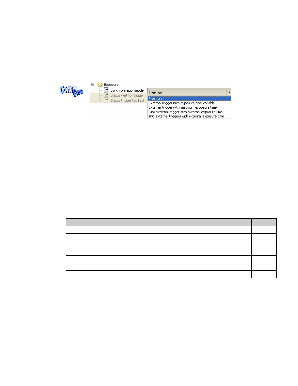
• Synchronisation Mode: Timed or Triggered, it defines how the grabbing is synchronized. This command is
available in the CommCam “Exposure” section :
Ö Read function : “r sync”;
Return by the camera:
• 0 : Free Run mode
• 1 : Ext Trig with Integration time set in the Camera
• 2 : Ext Trig with Integration time maximum in the line period
• 3 : Ext ITC (Integration Time Controlled) : The same Trig signal defines the line period
and its low level defines the integration time
• 4
: Ext Trig with two trig signal : CC2 defines the start of the integration and CC2 defines
the Stop of the integration.
Ö Write function : “w sync” <value>
o Timing Specifications
This table is for all the synchronization modes.
Label Description Min Typ Max
ti Effective exposure time duration 1,5 µs - -
td CC1 rising to integration period start delay 0.3 µs
ts Integration period stop to LINE1 rising set-up time 2.0 µs
th CC1 hold time (pulse high duration) 1 / 3 µs
(*)
td1 CC1/CC2 falling/rising to integration period start delay 0.3 µs
td2 CC1/CC2 rising to integration period stop delay 0.3 µs
tcc CC1 Rising to integration stop delay 3µs
(*)
3µs in ITC Trig Mode, 1µs for the other modes

ELiiXA® UC8/UC4
29
Eliixa_Color–revF 04/11
e2v semiconductors SAS 2011
Exposure Mode Timed : Free Run
This mode doesn’t require an external trigger.
In this case, the line period (Lp) can be defined in the Camera (see below) but the real line
period of the camera depends also on the exposure time (Texp) set:
- If Texp > Lp, the line period is equal to Texp
- If Lp > Texp, the line period is equal to Lp
INTEGRATION N
READOUT N-1 READOUT N
INTEGRATION N+1
ti
Ext Trig with integration time set in the camera
This mode requires an external trigger ( via CC1) but the exposure time is the one defined
in the Camera.
If the line period of the Trig signal provided to the camera is bigger than the exposure time set
in the camera, the “short trig pulses” will be ignored : The exposure set in the camera defines
the minimum line period possible.
INTEGRATION N INTEGRATION N+1
READOUT N
CC1
td
th
ts
ti
Ext Trig Full Integration time available
This mode requires an external trigger (via CC1). The exposure time is the maximum
possible value between two Tri pulses.
In this mode, the exposure time set in the camera is ignored.
Avoid this mode if your trigger is not stable (variable line period) : The exposure of each line
could then be different.
If the period of the trig signal is less than the readout time, the Camera won’t send any signal.

ELiiXA® UC8/UC4
30
Eliixa_Color–revF 04/11
e2v semiconductors SAS 2011
INTEGRATION N INTEGRATION N+1
REA DOU T N
CC1
td
th
Ti=LP
READOUT N-1
Lp
Ext Trig with Integration Time Controlled (ITC) with one Trig
This mode requires an external trigger ( via CC1). Both exposure time and line period are
defined by this Trig signal :
- The exposure time during the low level of the Trig Signal
- The line period between two rising edges of the Trig Signal
INTEGRATI ON N INTEGRATI ON N+1
RE ADOUT N- 1
CC1
th
READO UT N
ti
td1 td2
Ext Trig with Integration Time Controlled (ITC) with two Trigs
This mode requires two external triggers ( via CC1 and CC2):
- CC2 controls the starting of the exposure time
- CC1 controls the end of the exposure time.
The line period is defined by the one of the CC2 Trig signal.
td1
INTEGRATI ON N I NT EGRATI ON N+1
READOUT N
CC2
CC1
ti
td2
READOUT N-1

ELiiXA® UC8/UC4
31
Eliixa_Color–revF 04/11
e2v semiconductors SAS 2011
• Exposure time: Defines the integration time when set in the Camera. This command is available in the
CommCam “Exposure” section :
Ö Read function : “r tint”;
Return by the camera : Integer from 1 to 65535 (=0,1µs to 6,5535ms)
Ö Write function : “w tint” <value> ;
This value of integration time is taken in account only when the synchronisation mode is “free run” (0) or
“Ext Trig with Integration time set” (1). Otherwise it’s ignored.
• Line Period
: Defines the Line Period of the Camera in Timed mode. This command is available in the
CommCam “Exposure” section :
Ö Read function : “r tper”;
Return by the camera : Integer from 1 to 65535 (=0,1µs to 6,5535ms)
Ö Write function : “w tper” <value> ;
The line period is active only in Free Run mode. It’s also disabled if in this mode, the Integration time is
set higher than the Line Period.
The Line frequency indication (line per second) is calculated as : 1/Line Period.

ELiiXA® UC8/UC4
32
Eliixa_Color–revF 04/11
e2v semiconductors SAS 2011
Title Command Features
w sync 0 Set free run mode, with integration time and line period
programmable
w sync 1 Set line period synchronisation with integration time
programmable
w sync 2 Set line period synchronisation (start and period) with
integration time to its maximum
w sync 3 Set line period synchronisation (start and period) and
integration time controlled by 1 signal (ITC)
w sync 4 Set line period synchronisation (start and period) and
integration time controlled by 2 signals
Synchronisation Mode
r sync Get current synchronisation mode
w tint <val> Set integration time to <val> x100ns, from 1 to 65535 Integration time
r tint Get current integration time
w tper <val> Set line period to <val> x100ns, from 1 to 65535
Disabled if tper < tint
Line Period
r tper Get current line period
ELiiXA® UC8/UC4
33
Eliixa_Color–revF 04/11
e2v semiconductors SAS 2011
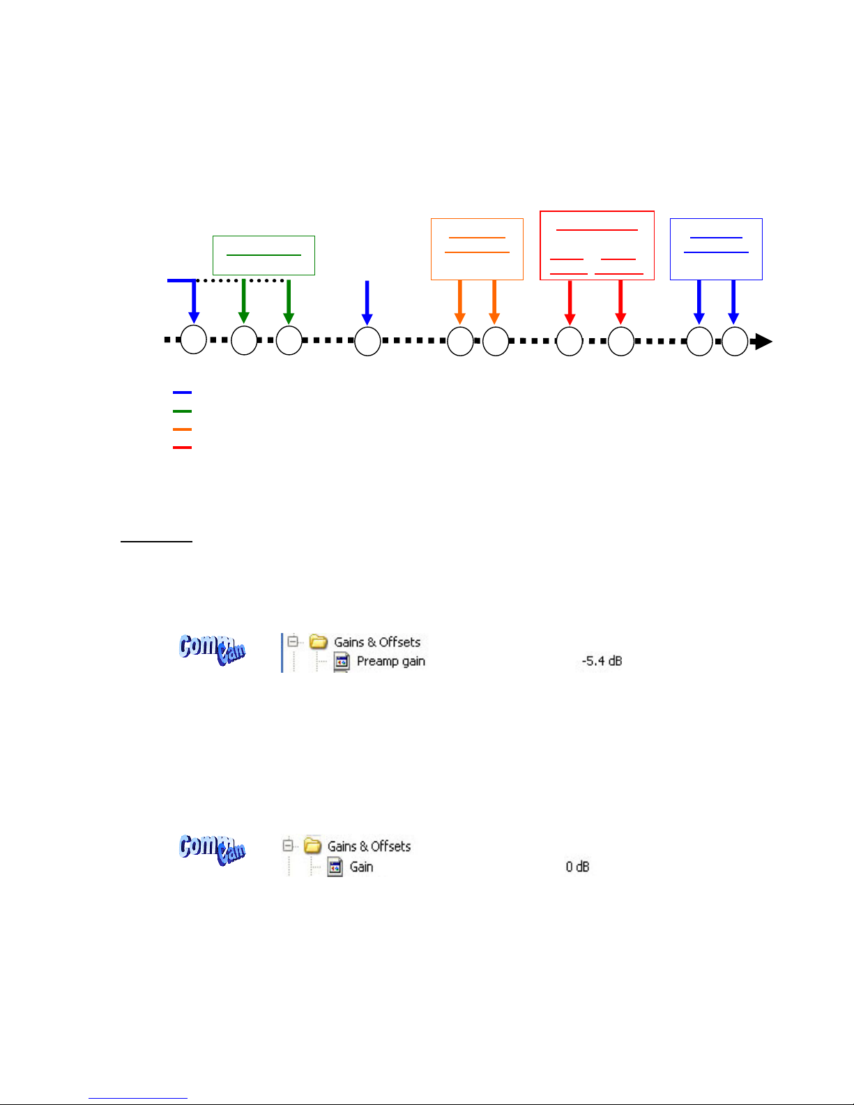
6.3.4 Gain and Offset
Ultimate Concept: A different way to set the Gain in order to improve the Tap balance
The “U” Concept has been developed to get a real improvement in term of tuning for the multi-Tap sensors :
As each sensor tap is driven by a different analog Chain, for an increasing of the global gain of the Camera,
each tap can have a different behavior on its own Gain and offset.
This means that to be perfectly adjusted, a balance of the taps should be performed ideally after each change
of the Gain.
The Ultimate Concept offers a solution as following:
The Global analog Gain of the Camera is divided in 2 parts :
o A preamp-Gain which is composed of several steps (4 x steps of 1,8dB on the ELIIXA)
o An amplification Gain with a continuous tuning (from -8,3dB to +14dB on the ELIIXA)
At each step of Preamp Gain, a Tap balance has been performed in factory for both Gains and Offsets and
saved in ROM memory. When a new value of Preamp Gain is set, the factory settings of the both Gain and
offset balance is automatically reloaded.
The user might also perform his own balance (automatically or manually) and can save it in one of the four
dedicated memory banks.
After the Preamp Gain level, the user can add more gain by using the Amplification Gain:
Ö
The best tuning is when the Amplification Gain is at its minimum possible
Ö
Each change of Preamp Gain value loads automatically the associated values of the Tap balance (Gain and
offset for each sensor tap).
This action takes more time than simply changing the Amplification Gain
Pre Am
p
0
0
--11,,88
--33,,66
--55,,44
Amp Gain (–8,3 to +14 dB)
--1133,,77ddBB
++88,,66ddBB
--1111..99ddB
B
++1100..44ddBB
--1100,,11ddB
B
++1122,,22ddBB
--88..33ddB
B
++1144ddB
B
ELiiXA® UC8/UC4
34
Eliixa_Color–revF 04/11
e2v semiconductors SAS 2011
The Global Chain of Gain is described as follows:
The Flat Field correction and the Color Modules will be detailed in a following chapter.
Analog Gain
• Preamp Gain
: Set the Pre-amplification Gain. This command is available in the CommCam “Gain & Offset”
section :
Ö Read function : “r pamp”;
Return by the camera: Integer corresponding to one of the different step values:
0 (-5.4dB), 1 (-3.6dB), 2 (-1.8dB) or 3 (0dB)
Ö Write function : “w pamp” <int> ;
• Gain
: Set the Amplification Gain. This command is available in the CommCam “Gain & Offset” section :
Ö Read function : “r gain”;
Return by the camera: Value from -237 to 416 corresponding to a Gain range of -8,32dB to
14,6dB by step of 0,0351dB
Ö Write function : “w gain” <int> ;
x
Amplification
Gain
x
Preamp
Gain
x
Tap Balance
Offset Gain
+
x
+
Flat Field
Correction
Offset Gain
x
+
Contrast
Expansion
Offset Gain
Color Module
Color
White
Matrix
Balance
x x
CCD
Global action
Action per Sensor Tap
Action per pixel
Action per color

ELiiXA® UC8/UC4
35
Eliixa_Color–revF 04/11
e2v semiconductors SAS 2011
Tap Balance
How to perform a Tap Balance ?
Why and when performing a Tap Balance?
Each output of the sensor (Tap) has its own analog Chain and behavior. There could have some discrepancies
between these outputs in extreme conditions of Gain or temperature
The Tap balance is already performed in factory for each level of Preamp-Gain. If necessary, the Tap balance
can be performed again by the User on both Offsets and Gains
The Procedure is the following :
Tap Balance by Offsets
¾ Cover the Lens of the camera to get a dark uniform target. This is not recommended to perform an
Offset balance under light conditions.
¾ Launch the Tap Offset Balance
¾ The process takes a few seconds and can be interrupted when you want
Tap Balance by Gains
¾ Choose the color line on which you’ll perform the Gain balance
¾ Provide an uniform light target to the camera: This is recommended to have a global level of around at
least 70% of the saturation, otherwise, with a low light level (< 30% of the Saturation) the Gain has
less effect than the Offset and your balancing won’t be efficient.
¾ Launch the Tap Gain Balance
¾ The process takes a few seconds and can be interrupted when you want
¾ You can save the result in memory (result for both Gains and offsets).
Internal Process
During the calibration process, the Camera calculates averages on some strategic ROIs (around the junction
between taps) and then estimates the slope of the tangents and then the projections on each side of the
junction.
The adjustment between these two neighbor taps is calculated to cancel the difference between the two
projections (right and left).
Right projection
Left projection Average area
Pixel value
Average area
distance
Average
area width

ELiiXA® UC8/UC4
36
Eliixa_Color–revF 04/11
e2v semiconductors SAS 2011
• Offsets and Gain Taps Balance
: All the commands are available in the CommCam “Gain & Offset” section
:
• Offsets Balance:
Ö Read function: “r balo”;
Returns the Offset Balance status: 1 for running and 0 for stopped.
Ö Write function :
“w balo 1” : Starts the offset balance. The value switches back to 0 automatically
when the balance process is finished (“Offset Balance control” in CommCam)
“w balo 0” : Stops the offset balance. No action if the process is already finished
(“Abort Offset balance Control” in CommCam).
• Gains Balance
:
o Choice of the color line
In CommCam
, the Choice of the line(s) is done through two different commands :
Red, blue or green or a combination of these 3 colors.
Choice of the Fourth line:
Each of these commands is followed by the reading of the Gain Balance Status.
The final combination of choice will be taken in account in the launching of the Gain balance
o Tap Gains balance Control
Ö Read function : “r balg”;
Returns the Tap Balance status: 0 if finished.
Ö Write function :
“w balg <val>”: Starts the offset balance.
<Val> is a combination (Xor or Sum) of the different color lines on which the balance
will be performed:
<val>=1: Red =1; Blue = 2; Green = 4; Nir/Mono = 8.

ELiiXA® UC8/UC4
37
Eliixa_Color–revF 04/11
e2v semiconductors SAS 2011
For example val = 14 means that the lines Blue + Green + Nir (or Mono) will be
processed.
The value switches back to 0 automatically when the balance process is finished (“Gain
Balance control” in CommCam)
“w balg 0” : Stops the Gain balance. No action is the process is already finished
(“Abort Gain balance Control” in CommCam).
• Tap Balance Bank Management
: The new-processed Tap balance can be saved in 4 x User banks (both
Gains and Offsets in the same time).
Ö Read function
“r rbal” : Get the current Tap Bank used (0: Factory or 1 to 4)
“w rbal <val>” : Load Tap Bank from bank <val> (0: Factory or 1 to 4)
Ö Write function :
“w sbal <val>” : Save the current Tap Balance in the User bank <val> (1 to 4)
Contrast Expansion
• Digital Gain
: Set the global Digital Gain. This command is available in the CommCam “Gain & Offset”
section :
Ö Read function : “r gdig”;
Returned by the camera : Value from 0 to 255. The corresponding Gain is calculated as
20log(1+val/64) in dB
Ö Write function : “w gdig” <int> ;
• Digital Offset
: Set the global Digital Offset. This command is available in the CommCam “Gain & Offset”
section :
Ö Read function : “r offs”;
Returned by the camera : Value from –4096 to +4095 in LSB
Ö Write function : “w offs” <int> ;

ELiiXA® UC8/UC4
38
Eliixa_Color–revF 04/11
e2v semiconductors SAS 2011
Title Command Features
w pamp <val> Set pre amplifier gain to: 0 (-5.4dB), 1 (-3.6dB), 2 (-1.8dB), 3
(0dB) (analog gain)
Change Tap balance settings to factory default
Preamp gain
r pamp Get current pre amplifier
w gain <val> Set gain form –8.32dB (-237) to +14.60dB (+416)
step of 0.0351dB
Gain
r gain Get current gain
w balo 1 Start offset tap balance; OnePush button (auto disable once
finished)
w balo 0 Stop offset tap balance
r balo Get the offset tap balance status
w balg <val> Start gain tap balance; OnePush button (auto disable once
finished)
• <val>=1: Red
• <val>=2: Blue
• <val>=4: Green
• <val>=8: NIR
<val> can be Combined with different values
w balg 0 Stop gain tap balance
Tap Balance
r balg Get the gain tap balance status
(1 for running, 0 for finished).
w sbal <val> Save current Balance tap into bank number <val>.
<val> between 1 and 4
w rbal 0 Load current Balance tap from factory bank (0)
w rbal <val> Load current Balance tap from bank number <val>.
<val> between 1 and 4
Balance Tap bank
r rbal Get the current Balance tap bank used (saved or loaded)
w gdig <val> Set digital gain from 0 to 255 (20log(1+val/64) dB) Digital Gain
r gdig Get digital gain
w offs <val> Set global offset from –4096 to +4095 in 12bits LSB (numeric
offset)
Digital Offset
r offs Get global offset

ELiiXA® UC8/UC4
39
Eliixa_Color–revF 04/11
e2v semiconductors SAS 2011
6.3.5 Color Management
White Balance
How is performed the White Balance ?
Automatic White Balance Calculation
The User can access to one dedicated Gain per color line (R, G, B and eventually Mono or NIR).
The Red, Green and Blue Gain are used to perform the “White Balance”.
The ELIIXA embeds an automatic function to calculate the appropriate Gains for a perfect white balance.
This Auto white balance affects only the Red, Green and Blue Gains (not the Mono or Nir of the 4x Lines
versions).
When this function is launched, the Camera calculates the average value for each color line in a ROI of 512
pixels located in the centre of the CCD :
Each gain is then calculated to reach the level of the color which has the highest sensitivity.
Note: After an automatic White Balance with CommCam, the 3 colors gains values are not refreshed in the
CommCam Interface.
How to perform the White Balance?
The User has to propose a white target to the Camera.
The Global Gain of the Camera has to be set to avoid saturation in any of the 3 x RGB colors.
The Color Matrix must be enabled if you’re using a RGB+Nir Camera version.
The White Balance can be enabled before: During the calculation process it is disabled automatically.
¾ The User has to propose a white target to the Camera.
¾ Set the global Gain to avoid saturation and disable the color Matrix.
¾ Launch the auto WB calibration
¾ Enable the White Balance : The new coefficients are now active
¾ Adjust the Gain of the fourth line (Mono or Nir) if present
¾ Save the result in one of the 4 x user banks dedicated to the color management.
Pixel value
Average
blue
Red
Green
ROI

ELiiXA® UC8/UC4
40
Eliixa_Color–revF 04/11
e2v semiconductors SAS 2011
• Auto White Balance Activation: Activate the White balance. This command is available in the CommCam
“Color Management” section :
Ö Read function : “r wben” : Returns the White balance Status (0 if disabled, 1 if enabled)
Ö Write function :
“w wben 1”: Enable the white Balance : The Color Gains are now activated.
“w wben 0” : Disable the white Balance
• Auto White Balance Calibration
: Launch the Auto WB calculation process. This command is available in
the CommCam “Color Management” section :
Ö Read function : “r sawb” : Returns the Auto White balance process Status (0 if off, 1 if
active)
Ö Write function :
“w sawb 1” : Launch the Auto white Balance calibration process.
“w sawb 0” : Abort the Auto white Balance calibration process. No effect if already
stopped.
• Manual White Balance
: Access to the RGB +Mono or Nir Gains. These commands are available in the
CommCam “Color Management” section :
o White Balance Red Gain
Ö Read function : “r wbar <val>” : Returns the White balance Red Gain value.
Ö Write function : “w wbar <val>” : Sets the White balance Red Gain value.
<val> is a Q13.10 unsigned value (from 0 to 7,999…).
The Red Gain is calculated and displayed as follow : WBr = 1 + <val>
o White Balance Green Gain
Ö Read function : “r wbag <val>” : Returns the White balance Green Gain value.
Ö Write function : “w wbag <val>” : Sets the White balance Green Gain value.
<val> is a Q13.10 unsigned value (from 0 to 7,999…).
The Green Gain is calculated and displayed as follow : WBg = 1 + <val>
ELiiXA® UC8/UC4
41
Eliixa_Color–revF 04/11
e2v semiconductors SAS 2011
o White Balance Blue Gain
Ö Read function : “r wbab <val>” : Returns the White balance Blue Gain value.
Ö Write function : “w wbab <val>” : Sets the White balance Blue Gain value.
<val> is a Q13.10 unsigned value (from 0 to 7,999…).
The Blue Gain is calculated and displayed as follow : WBb = 1 + <val>
o White Balance Nir or Mono Gain (non available on RGB versions)
Ö Read function : “r wbai <val>” : Returns the White balance Nir/Mono Gain value.
Ö Write function : “w wbai <val>” : Sets the White balance Nir/Mono Gain value.
<val> is a Q13.10 unsigned value (from 0 to 7,999…).
The Nir/Mono Gain is calculated and displayed as follow : WBi = 1 + <val>
Color Matrix
What is the interest of the Color Matrix ?
After white balancing, the color space correction shall be done to improve the color response. This correction
consists in a linear operation to convert the RGB triplet form the camera color space to the RGB triplet of
the final color space. The final color space can be a monitor, a printer or others application specific color
space. For some specific applications where "absolute" color value is not mandatory the color space correction
can be bypassed.
R” cm11 cm12 cm13 cm14 R’
B” cm21 cm22 cm23 cm24 B’
G” cm31 cm32 cm33 cm34 G’
N” cm41 cm4é cm43 cm44 N’
Each coefficient can be set in the following limits : -4 to +3,999
The last line and column are valid only for the RGB + Nir Version.
They are available for the RGB + Mono but have no signification for the color space tuning.
Attention = This Matrix is shown here in the real order of the CCD color lines : Red, Blue and Green + 4th and
not the usual order: R,G,B.
Then for Commcam:
¾ the “cm1x” define the first line or the “Red Line”, “cm2x” the Blue line, cm3x the Green line and cm4x
the Nir Line.
¾ “cmx1” define the Red column, cmx2 the Blue column, cmx3 the Green column and cmx4 the Nir
column.

ELiiXA® UC8/UC4
42
Eliixa_Color–revF 04/11
e2v semiconductors SAS 2011
The default Matrix are the following :
¾ For the RGB+Nir Versions:
1 0 0 -1
0 1 0 -1 To remove the Nir Infra Red component of each color and which has
0 0 1 -1 been measured with the Nir Line
0 0 0 1
Some values of the RGB Matrix will be proposed in
Appendix C for different type of light source.
The Sum of the 3 parameters of the RGB Matrix on the same line must be equal to 1 in order to
avoid changing the White Balance.
¾ For the RGB or RGB+Mono Versions:
1 0 0 0
0 1 0 0 Not Available for the RGB Version.
0 0 1 0
0 0 0 1
Some values of the RGB Matrix will be proposed in
Appendix C for different type of light source.
• Color Matrix Enable
: Activates the color Matrix. This command is available in the CommCam “Color
Management” section :
Ö Read function : “r come” : Returns the Color matrix Status (0 if disabled, 1 if enabled)
Ö Write function :
“w come 1” : Enable the color Matrix.
“w come 0” : Disable the color Matrix
• Color Matrix coefficients
: To set each of the Color Matrix coefficients. This command is available in
the CommCam “Color Management / Manual Matrix” section :

ELiiXA® UC8/UC4
43
Eliixa_Color–revF 04/11
e2v semiconductors SAS 2011
By clicking on “Click for extended control” we can get a global view of the Matrix :
Ö Read function : “r cm<line><column>” : Returns the value of the designed coefficient.
<line> and <column> are defined as follow : 1=Red, 2=Blue, 3=Green, 4=Nir or Mono (if exists)
Ö Write function : “w cm<line><column> <val>” : sets the coefficient of the matrix.
<line> and <column> are defined as follow : 1=Red, 2=Blue, 3=Green, 4=Nir or Mono (if
exists)
<val> is is from –4096 to +4095. (gain format Q13.10 signed)
The coefficient associated to <val> is calculated as follow : cm = <val>/1024

ELiiXA® UC8/UC4
44
Eliixa_Color–revF 04/11
e2v semiconductors SAS 2011
• Save & restore color settings: Allows saving or restoring all the colors settings: White balance gains and
colors matrix coefficients. This command is available in the CommCam “Color Management” section :
Ö Read function
“r rcol” : Get the current Tap Bank used (0: Factory , 1 to 4 for User, 5 for
Integrator)
“w rcol <val>” : Load Tap Bank from bank <val> (0: Factory , 1 to 4 for User, 5 for
Integrator)
Ö Write function :
“w scol <val>” : Save the current Tap Balance in the User bank <val> (1 to 4 for User, 5
for Integrator)

ELiiXA® UC8/UC4
45
Eliixa_Color–revF 04/11
e2v semiconductors SAS 2011
Title Command Features
w sawb 1 start auto white balance
w sawb 0 stop auto white balance
Auto White balance
calibration
r sawb auto white balance state
w wben 0
w wben 1
white balance disable
white balance enable
White balance activation
r wben Get white balance state
w wbar <val> Set red white balance coefficient
<val> from 0 to 8191.
Red gain format 1+<val> (representation <val>: Q13.10
unsigned)
White Balance Red
r wbar get red white balance coefficient
w wbab <val> Set blue white balance coefficient
(same representation as wbar)
White Balance Blue
r wbab get blue white balance coefficient
w wbag <val> Set green white balance coefficient
(same representation as wbar)
White Balance Green
r wbag get green white balance coefficient
w wbai <val> Set NIR white balance coefficient
(same representation as wbar)
White Balance IR
r wbai get NIR white balance coefficient
w come 1
w come 0
Enable color matrix
Disable color matrix
Color matrix enable
r come read state of color matrix
w cm<l><c> <val>
Color matrix coefficient: its representation is:
cm11 cm12 cm13 cm14
cm21 cm22 cm23 cm24
cm31 cm32 cm33 cm34
cm41 cm42 cm43 cm44
<val> is from –4096 to +4095. (gain format Q13.10 signed)
l/c : 1=Red, 2=Blue, 3=Green, 4=Nir or Mono (if exists)
Color Matrix
r cm<l><c> read color matrix coefficient
w scol <val> Save current Color settings into bank number <val>.
<val> between 1 and 4 for User and 5 for Integrator
w rcol <val> Load current Color settings from bank number <val>.
<val> between 1 and 4 for User, O for factory default and
5 for Integrator
Color settings bank
r rcol Get the current Color settings bank used (saved or loaded)
ELiiXA® UC8/UC4
46
Eliixa_Color–revF 04/11
e2v semiconductors SAS 2011
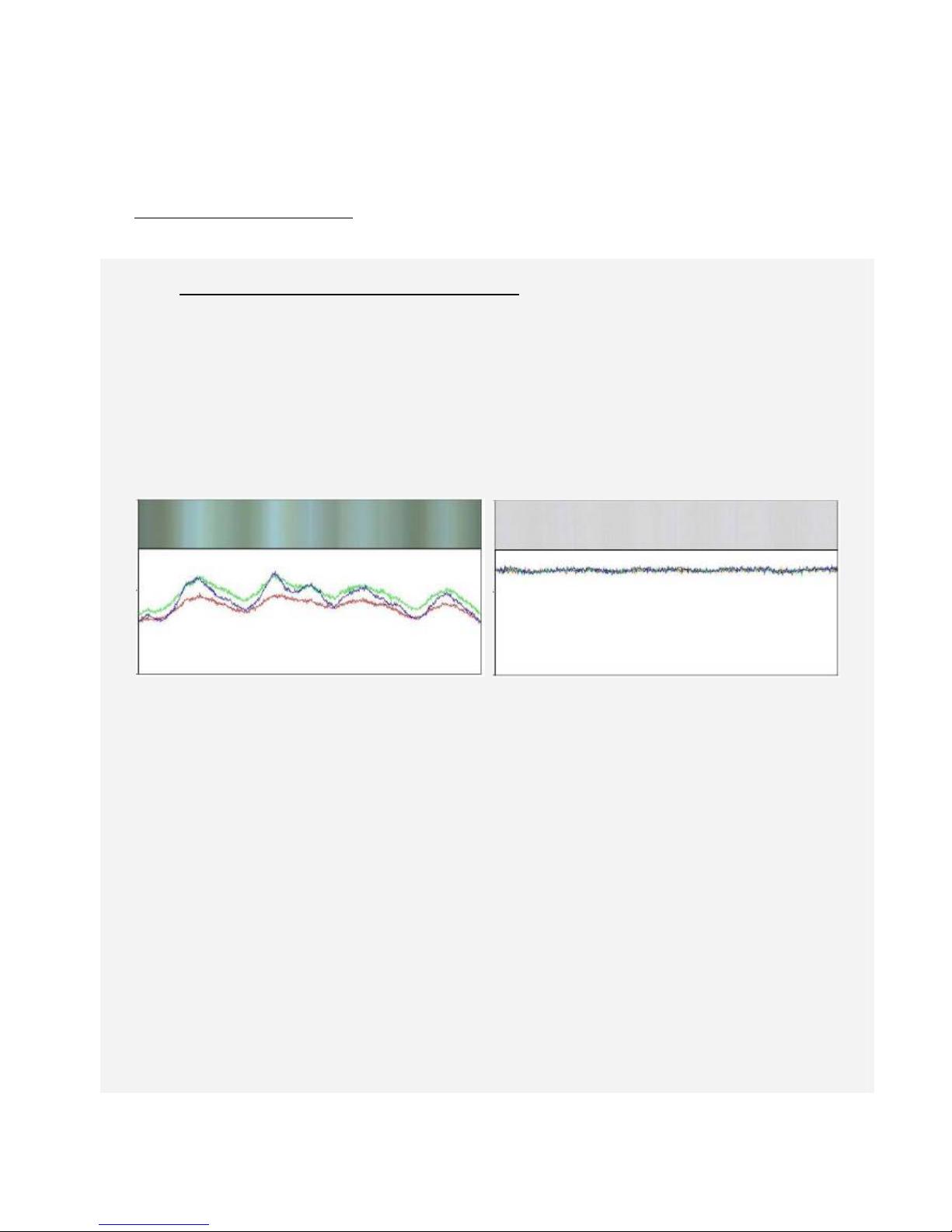
6.3.6 Flat Field Correction
Automatic Flat Field Correction
How is performed the Flat Field Correction?
What is the Flat Field correction (FFC)?
The Flat Field Correction is a digital correction on each pixel which allows :
¾ To correct the Pixel PRNU (Pixel Response Non Uniformity) and DSNU (Dark Signal Non
Uniformity)
¾ To Correct the shading due to the lens
¾ To correct the Light source non uniformity : The FFC on color is also specially efficient when your
Light source is non uniform in color (ex : LED source with some LEDs more blue and others more
red) :
Before After
How is calculated/Applied the FFC?
The FFC is a digital correction on the pixel level for both Gain and Offset.
¾ Each Pixel is corrected with :
o An Offset on 8 bits (Signed Int 5.3). They cover a dynamic of ±16LSB in 12bits with a
resolution of 1/8 LSB 12bits.
o A Gain on 14 bits (Unsigned Int 14) with a max gain value of x3
o The calculation of the new pixel value is : P’ = ( P + Off).(1 + Gain/8192)
¾ Each color line has its own independent FFC Calculation :
o For the offset, the average dark of each pixel is calculated to be subtracted as an offset
correction
o For the Gain, the Maximum of the color line is the reference and each pixel Gain is
calculated to reach this maximum: The Maximum correction possible is x3.

ELiiXA® UC8/UC4
47
Eliixa_Color–revF 04/11
e2v semiconductors SAS 2011
How to perform the Flat Field Correction?
FPN/DSNU Calibration
¾ Cover the lens
¾ Launch the FPN Calibration : Grab and calculation is performed in few seconds
PRNU Calibration
The User must propose a white uniform target to the Camera (not a fixed paper).
The Gain/Light conditions must give a non saturated image in any color.
The Camera must be set in the final conditions of Light/ Gain and in the final position in the System.
The White Balance and color Matrix can be enabled: They don’t affect the result. but after the FFC
calibration, the User will have to perform a new White Balance
¾ White uniform (moving) target
¾ Launch the FFC
¾ Enable the FFC
¾ You can save the FFC result (both FPN+PRNU in the same time) in one of the 4 x FFC User Banks.
Advices
The ELIIXA has 4 x FFC Banks to save 4 x different FFC calibrations. You can use this feature if your
system needs some different conditions of lightning and/or Gain because it’s looking for different targets:
You can perform one FFC per condition of Gain/setting of the Camera ( 4 Max) and recall one of the four
global settings (Camera Configuration + FFC + Color management) when required.
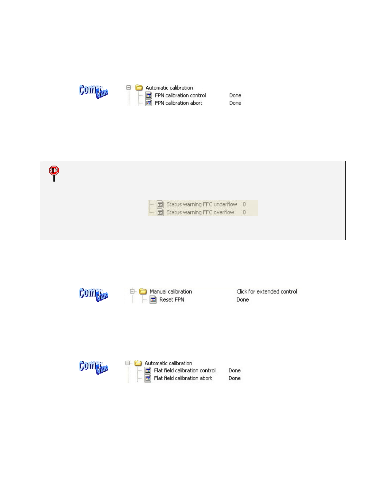
• FFC Activation: Enable/disable the Flat Field Correction. This command is available in the CommCam
“Flat Field Correction” section :
Ö Read function : “r ffcp” : Returns the FFC Status (0 if disabled, 1 if enabled)
Ö Write function :
“w ffcp 1”: Enable the FFC.
Pixel value
blue
Red
Green
Nir/Mono
ELiiXA® UC8/UC4
48
Eliixa_Color–revF 04/11
e2v semiconductors SAS 2011
“w ffcp 0”: Disabled the FFC
• FPN/DSNU Calibration
: Launches the FFC process for the Offsets calculation. This command is available
in the CommCam “Flat Field Correction/Automatic Calibration ” section:
Ö Read function : “r calo”: Returns the FPN Calculation Process Status (0 if finished, 1 if
processing)
Ö Write function :
“w calo 1” : Launch the FPN Calibration Process.
“w calo 0”: Abort the FPN Calibration Process.
Some Warnings can be issued from the FPN Calibration Process as “pixel underflow” because some pixel
have been detected at “0” level. The Calculation result will be proposed anyway as it’s just a warning
message.
This will change the Status Register which is displayed in CommCam :
The warning messages possible are detailed in the Appendix 6 (Table 2, §6.2).
• FPN coefficient Reset : Reset the FPN (Offsets) coefficient in Memory. This command is available in
the CommCam “Flat Field Correction / Manual Calibration ” section :
Ö Write function : “w rsto 0” : Reset (set to 0) the FPN coefficients in memory. This doesn’t
affect the FFC User Memory Bank but only the active coefficients in Memory.
• PRNU Calibration
: Launches the PRNU process for the Gains calculation. This command is available in
the CommCam “Flat Field Correction / Automatic Calibration ” section :
Ö Read function : “r calg”: Returns the PRNU Calculation Process Status (0 if finished, 1 if
processing)
Ö Write function :
“w calg 1”: Launch the PRNU Calibration Process.
“w calg 0”: Abort the PRNU Calibration Process.

ELiiXA® UC8/UC4
49
Eliixa_Color–revF 04/11
e2v semiconductors SAS 2011
• DSNU coefficient Reset : Reset the DSNU (Gains) coefficient in Memory. This command is available in
the CommCam “Flat Field Correction / Manual Calibration ” section :
Ö Write function : “w rstg 0” : Reset (set to 0) the FPN coefficients in memory. This doesn’t
affect the FFC User Memory Bank but only the active coefficients in Memory.
Some Warnings can be issued from the FPN Calibration Process as “pixel Overflow” because some
saturated pixel have been detected. The Calculation result will be proposed anyway as it’s just a warning
message.
This will change the Status Register which is displayed in CommCam :
The warning messages possible are detailed in the Appendix 6 (Table 2, §6.2).
Manual Flat Field Correction
The FFC Coefficients can also be processed outside of the Camera or changed manually by accessing directly
their values in the Camera : This is the “Manual” FFC.
In CommCam, the User can access to a specific interface by clicking on “click for extended control” in the
Manual FFC section :
This will allow the user to upload/download out/in the Camera the FFC coefficients in/from a text file that
can be processed externally.
It is recommended to setup the baud rate at the maximum value possible (115000 for example) otherwise
the transfer can take a long time.

ELiiXA® UC8/UC4
50
Eliixa_Color–revF 04/11
e2v semiconductors SAS 2011
• FPN coefficients modification : Direct access to the FPN coefficients for reading or writing. This
command is available in the CommCam “Flat Field Correction / Manual Calibration ” section :
⇒ Read function : “r ffco <addr> <nbrval> [crcreq]”: Read <nbrval> FPN user coefficients
starting from <addr> address. If [crcreq] is equal to 1, the crc will be calculated on the
outputted value.
<nbrval> is between 1 and 10
<addr> starts from
• 1 for Red coefficients
• 5001 for Blue Coefficients
• 10001 for Green coefficients
• 15001 for NIR Coefficients
Output is:
<val> …[crcval]
⇒ Write function :” w ffco <addr> <nbrval> <val> … [crcval]” : Write <nbrval> FPN user
coefficients starting from the <addr> address. If [crcval] is added, the crc value is computed
on the all the <val>. <val> is signed.
<addr> starts from
• 1 for Red coefficients
• 5001 for Blue Coefficients
• 10001 for Green coefficients
• 15001 for NIR Coefficients
<nbrval> is between 1 and 10
<val> is between –128 et +127
• PRNU coefficients modification
: Direct access to the PRNU coefficients for reading or writing. This
command is available in the CommCam “Flat Field Correction / Manual Calibration ” section :

ELiiXA® UC8/UC4
51
Eliixa_Color–revF 04/11
e2v semiconductors SAS 2011
⇒ Read function : “r ffcg <addr> <nbrval> [crcreq]” : Read <nbrval> FPN user coefficients
starting from <addr> address. If [crcreq] is equal to 1, the crc will be calculated on the
outputted value.
<nbrval> is between 1 and 10
<addr> starts from
• 1 for Red coefficients
• 5001 for Blue Coefficients
• 10001 for Green coefficients
• 15001 for NIR Coefficients
Output is:
<val> …[crcval]
⇒ Write function :” w ffcg <addr> <nbrval> <val> … [crcval]” : Write <nbrval> FPN user
coefficients starting from the <addr> address. If [crcval] is added, the crc value is computed
on the all the <val>. <val> is signed.
<addr> starts from
• 1 for Red coefficients
• 5001 for Blue Coefficients
• 10001 for Green coefficients
• 15001 for NIR Coefficients
<nbrval> is between 1 and 10
<val> is between 0 and 16383
• FFC User Bank Management
: The new-processed FFC can be saved in 4 x User banks (both Gains and
Offsets in the same time).
Ö Read function
“r rffc” : Get the current Tap Bank used (0: Factory or 1 to 4)
“w rffc <val>” : Load Tap Bank from bank <val> (0: Factory or 1 to 4)
Ö Write function :
“w rffc <val>” : Save the current Tap Balance in the User bank <val> (1 to 4)

ELiiXA® UC8/UC4
52
Eliixa_Color–revF 04/11
e2v semiconductors SAS 2011
Title Command Features
w ffcp 0 Disable Flat Field Correction processing
w ffcp 1 Enable Flat Field Correction processing
FFCorrection
r ffcp Get Flat Field Correction processing status
w calo 1 Start FPN user calibration; OnePush button (auto disable once
finished)
w calo 0 Stop FPN user calibration
FPN User Calibration
r calo Get the FPN user calibration status
w calg 1 Start PRNU user calibration for all colors; OnePush button
(auto disable once finished)
W calg 0 Stop PRNU user calibration
PRNU User Calibration
r calg Get the PRNU user calibration status
FPN Reset w rsto 0 Clear FPN coefficients to 0
PRNU Reset w rstg 0 Set PRNU coefficients to 1
w sffc <val> Save current user FFC (FPN & PRNU) into FFC bank number
<val>.
<val> between 1 and 4
w rffc <val> Load current user FFC from FFC bank number <val>.
<val> between 0 and 4
0 is a virtual bank that reset ffc coefficients
FFC user bank
r rffc Get the current user FFC bank used (saved or loaded)

ELiiXA® UC8/UC4
53
Eliixa_Color–revF 04/11
e2v semiconductors SAS 2011
Title Command Features
FPN user coefficients w ffco <addr>
<nbrval> <val> …
[crcval]
Write <nbrval> FPN user coefficients starting from the <addr>
address. If [crcval] is added, the crc value is computed on the
all the <val>. <val> is signed.
<addr> starts from
• 1 for Red coefficients
• 5001 for Blue Coefficients
• 10001 for Green coefficients
• 15001 for NIR Coefficients
<nbrval> is between 1 and 10
<val> is between –128 et +127
r ffco <addr>
<nbrval> [crcreq]
Read <nbrval> FPN user coefficients starting from <addr>
address. If [crcreq] is equal to 1, the crc will be calculated on
the outputted value.
<addr> starts from
• 1 for Red coefficients
• 5001 for Blue Coefficients
• 10001 for Green coefficients
• 15001 for NIR Coefficients
<nbrval> is between 1 and 10
Output is:
<val> …[crcval]
w ffcg <addr>
<nbrval> <val> …
[crcval]
Write <nbrval> PRNU user coefficients starting from the <addr>
address. If [crcval] is added, the crc value is computed on the
all the <val>.
<addr> starts from
• 1 for Red coefficients
• 5001 for Blue Coefficients
• 10001 for Green coefficients
• 15001 for NIR Coefficients
<nbrval> is between 1 and 10
<val> is between 0 and 16383
PRNU user coefficients
r ffcg <addr>
<nbrval> [crcreq]
Read <nbrval> PRNU user coefficients starting from <addr>
address. If [crcreq] is equal to 1, the crc will be calculate on
the outputted value.
<addr> starts from
• 1 for Red coefficients
• 5001 for Blue Coefficients
• 10001 for Green coefficients
• 15001 for NIR Coefficients
<nbrval> is between 1 and 10
Output is:
<val> …[crcval]

ELiiXA® UC8/UC4
54
Eliixa_Color–revF 04/11
e2v semiconductors SAS 2011
6.3.7 Save & Restore Settings
The settings (or Main configuration) of the Camera can be saved in 4 x different User banks.
¾ These settings don’t include neither the Color settings (White balance and Color Matrix) nor the Tap
Balance (Gains and offsets) nor the FFC which have each their own 4 User banks.
¾ These settings include user bank in use for each category: Tap Balance, Color Management, FFC. This
allow, by loading one Camera configuration at the startup to load also automatically the associated FFC
and color settings.
• Save & restore settings
: Allows to save or restore all the Camera settings : This command is available in
the CommCam “Save & Restore settings” section :
Ö Read function
“r rcfg” : Get the current Bank used (0: Factory , 1 to 4 for User, 5 for Integrator)
“w rcfg <val>” : Load settings from bank <val> (0: Factory , 1 to 4 for User, 5 for
Integrator)
Ö Write function :
“w scfg <val>” : Save the current Settings in the User bank <val> (1 to 4 for User, 5
for Integrator)
Title Command Features
w scfg 0 Save current configuration into factory bank (0) PAS DISPO
w scfg <val> Save current configuration into bank number <val>.
<val> between 1 and 4
w scfg 5 Save current configuration into integrator bank (5)
w rcfg 0 Load current configuration from factory bank (0)
w rcfg <val> Load current configuration from bank number <val>.
<val> between 1 and 4
w rcfg 5 Load current configuration from integrator bank (5).
Configuration
r rcfg Get the current configuration bank used (saved or loaded)

ELiiXA® UC8/UC4
55
Eliixa_Color–revF 04/11
e2v semiconductors SAS 2011
7 APPENDIX A: Camera Status Details
7.1 Table 1 : Processing Status
Name Init Value Update Description
Wait for trigger 0 Set to 1 when Camera in
triggered mode and no trigger
is received.
Otherwise, value set to 0
No trigger received since the last scan (1Hz).
Settings Modified 0 Set to 1 after any valid change
of a configuration parameter.
Set to 0 after each save or
restore action on a config
memory bank
Notify any change in the Camera parameters.
Saving in configuration User bank is necessary
to keep the new settings after the reboot of
the Camera
Tap Balance
Modified
0 Set to 1 after a valid change
of the Tap balance
Set to 0 after each save or
restore action on a tap balance
memory bank
Notify any change in the current Camera tap
balance.
Saving in tap balance User bank is necessary to
keep the new settings after the reboot of the
Camera
Processing Status
FFC Modified 0 Set to 1 after a valid change
of a FPN or PRNU coefficient
Set to 0 after each save or
restore action on a FFC
memory bank
Notify any change in the current Camera
FFC parameters.
Saving in FFC User bank is necessary to keep
the new settings after the reboot of the
Camera
7.2 Table 2 : Internal Task Status
Name Init Value Update Description
Warn Ovf 0 At each end of calibration /
Tap balance / White balance
Notify that an Overflow occurred during a
calibration (FFC, Tap Balance, White Balance) :
Logical OR of all the FPGA flags
The result of the calibration is nevertheless
available
Warn Udf 0 At each end of calibration /
Tap balance / White balance
Notify that an Underflow occurred during a
calibration (FFC, Tap Balance, White Balance) :
Logical OR of all the FPGA flags
The result of the calibration is nevertheless
available
Internal Task Status
Cal/App Enabled 0 At each start and end of
calibration / Tap balance /
White balance
Notify that the Calibration (FFC, Tap Balance,
White Balance) is :
Active (1)
Or terminated (0)

ELiiXA® UC8/UC4
56
Eliixa_Color–revF 04/11
e2v semiconductors SAS 2011
7.3 Table 3 : Error Diagnostic Status
Name Init Value Update Description
Err hardware init 0 At each camera start or
when the FPGA restart
Notify that an error has occurred during the
hardware init of the camera :
Mainly the loading of the FPGA with a invalid or
corrupted dataflash contains.
Err factory
application settings
0 At the Camera startup Notify that an error is detected in one
parameters of the "Factory Application
Settings" EEPROM area
Err user application
settings
0 At the Camera startup Notify that an error is detected in one
parameters of the "User Application Settings"
EEPROM area
Err factory camera
settings
0 At the Camera startup or
each factory default
settings reload action
Notify that an error is detected in one
parameters of the "Factory Camera Settings"
EEPROM area
Err user camera
settings
0 At the Camera startup or
each User settings reload
action
Notify that an error is detected in one
parameters of the "User Camera Settings"
EEPROM area
diagnostic error Status
Err CommCam
compatibility index
0 At each read / write of
the Camera hardware ID
Notify that an error is detected in the
“CommCam compatibility index" EEPROM area

ELiiXA® UC8/UC4
57
Eliixa_Color–revF 04/11
e2v semiconductors SAS 2011
8 APPENDIX C : Thermal Management
The most important source of heat in the camera is around the sensor. The fastest version dissipates around
14W with 8 taps at 40MHz on the sensor.
The Camera has been designed to dissipate the maximum of the internal heat through its front face: The
packaging of the sensor is larger to increase the surface in contact with the front face and then improves the
dissipation.
In the system, the camera has to be fixed by its front face with the largest contact possible with a metallic
part.
Without any specific cooling system, a simple air flow around the camera will improve roughly the dissipation.
If necessary, additional heat sinks are available (reference below) and they can be fixed on any side of the
front face:
Set of 2 x Heat Sinks: Part number AT71KFPAVIVA-CAA
One heat sink can decrease the temperature of the front face of about 5°C down.

ELiiXA® UC8/UC4
58
Eliixa_Color–revF 04/11
e2v semiconductors SAS 2011
9 APPENDIX E: Optical Mounts available
F Mount: Kit10 (Part number AT71KFPAVIVA-ABA)

ELiiXA® UC8/UC4
59
Eliixa_Color–revF 04/11
e2v semiconductors SAS 2011
M42x0,75 (T2 Mount): Kit30 (Part number AT71KFPAVIVA-AKA)
M42x1 Mount: Kit40 (Part number AT71KFPAVIVA-ADA)

ELiiXA® UC8/UC4
60
Eliixa_Color–revF 04/11
e2v semiconductors SAS 2011
APPENDIX F: Color Matrix Examples
Please, contact the Camera hotline : hotline-cam@e2v.com for more information

ELiiXA® UC8/UC4
61
Eliixa_Color–revF 04/11
e2v semiconductors SAS 2011
10 APPENDIX G: Revision History
Revision
Comments / Details Camera Ref
Rev A
Preliminary release Firmware 2.0.0
Rev D
Spatial correction extended to 0,5 and 1,5 values + inhibition
Mechanical drawing detailed
Reverse/forward = 0/1 and explanation drawing
Firmware 3.0.0
Rev E
Status command
Mechanical drawing detailed for Mounts
Baud Rate change warning
Firmware 3.0.0
Rev F
Dual Base Interlaced 8bits output mode for BA0 only Firmware 3.0.2

ELiiXA® UC8/UC4
62
Eliixa_Color–revF 04/11
e2v semiconductors SAS 2011
How to reach us
Home page: www.e2v.com
Sales Office:
Northern Europe
e2v ltd
106 Waterhouse Lane
Chelmsford
Essex
CM1 2QU
England
Tel: +44 (0)1245 493493
Fax: +44 (0)1245 492492
E-Mail: enquiries@e2v.com
Southern Europe
e2v
sas
16 Burospace
F-91572 Bièvres
Cedex
France
Tel: +33 (0) 1 60 19 55 00
Fax:+33 (0) 1 60 19 55 29
E-Mail: enquiries-fr@e2v.com
Germany and Austria
e2v
gmbh
Industriestraße 29
82194 Gröbenzell
Germany
Tel: +49 (0) 842 410 570
Fax:: +49 (0) 842 284 547
E-Mail: enquiries-de@e2v.com
Americas
e2v inc.
4 Westchester Plaza
Elmsford
NY 10523-1482
USA
Tel: +1 (914) 592 6050
Fax:: +1 (914) 592-5148
E-Mail: enquiries-na@e2v.com
Asia Pacific
e2v
ltd
11/F.,
Onfem Tower,
29 Wyndham Street,Central,
Hong
Kong
Tel: +852 3679 364 8/9
Fax: +852 3583 1084
E-Mail: enquiries-ap@e2v.com
Product Contact:
e2v
Avenue de Rochepleine
BP 123 - 38521 Saint-Egrève Cedex
France
Tel: +33 (0)4 76 58 30 00
Hotline:
hotline-cam@e2v.com
 Loading...