DYNEX XT2116-801, XT2116-1601, XT2116-1401, XT2116-1201, XT2116-1001 Datasheet

XT2116
XT2116
Fast Turn-on Asymmetric Thyristor
Advance Information
Replaces March 1998 version, DS4674-2.2 DS4674-3.0 January 2000
APPLICATIONS
■ Pulse Modulators
■ Laser Diode Triggering
■ Capacitor Discharge Applications
FEATURES
■ The XT2116 is Asymmetrical Thyristor in which the
reverse voltage capability has been sacrificed to enable a
high forward blocking characteristic combined with
excellent turn-on performance.
■ Designed for rapid and efficient switching of high
current pulses.
VOLTAGE RATINGS
Type Number Max. Rise Time
t
r
(T
= 25˚C)
case
ns
XT2116 - 1601
XT2116 - 1401
XT2116 - 1201
XT2116 - 1001
XT2116 - 801
100
120
120
140
160
Repetitive Peak Voltage
V
DRM
V
1600
1400
1200
1000
800
KEY PARAMETERS
V
DRM
I
T(AV)
I
TSM
dIdt 2000A/
dV/dt 300V/µs
t
on
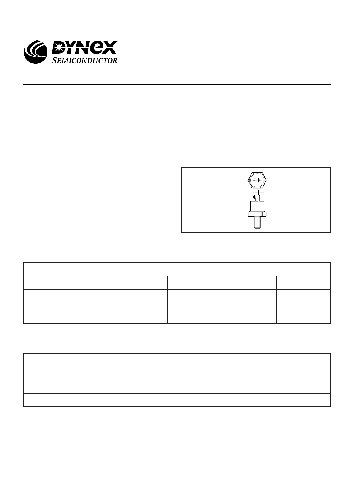
Outline type code: SO28.
See Package Details for further information.
Peak Working Voltages
V
RRM
V
< 2
< 2
< 2
< 2
< 2
*
V
DWM
V
1600
1400
1200
1000
800
1600V
50A
800A
µs
350ns
V
*
RWM
V
< 2
< 2
< 2
< 2
< 2
CURRENT RATINGS
Symbol Parameter Conditions UnitsMax.
I
T(AV)
I
T(RMS)
I
Mean on-state current
RMS value
T
Continuous (direct) on-state current
Half wave resistive load, T
= 80oC79A
T
case
T
= 85oC68A
case
= 80oC50A
case
1/4

XT2116
SURGE RATINGS
Symbol
I
TSM
2
tI
I
Parameter
Surge (non-repetitive) forward current
2
t for fusing 3200 A2s
10ms half sine; T
Conditions Max. Units
= 125oC
case
THERMAL AND MECHANICAL DATA
Symbol Parameter
th(j-c)
th(c-h)
T
vj
T
stg
- 3.5
Thermal resistance - junction to caseR
Thermal resistance - case to heatsinkR
Virtual junction temperature
Storage temperature range
Mounting torque
d.c.
Mounting torque 3.5Nm
with mounting compound
On-state (conducting) - 125
* Recommended value.
Conditions Min. Max. Units
DYNAMIC CHARACTERISTICS
800 A
- 0.35
0.25-
-55 125
*
4.0 Nm
o
C/W
o
C/W
o
o
C
C
T
= 25˚C unless otherwise stated.
case
ParameterSymbol Conditions
V
TM
I
RRM/IDRM
Maximum on-state voltage At IT = 100A
Peak reverse and off-state current At V
RRM/VDRM
dV/dt Maximum linear rate of rise of off-state voltage Tj = 125oC, To V
Half sine wave of 2µs, Tj = 125˚C
Gate source 20V, 10Ω. tr = 160ns
I
L
I
H
t
d
q
†
Available to 10µs.
Latching current -
Holding current -
Delay time VD = 400V, gate source = 500mA, tr = 50ns
I
Circuit commutated turn-off timet
= 25A, VRM = 0V, VDR = V
T
R
= 47Ω, dV/dt = 100V/µs.
GK
, RGK = 47Ω
DRM
DWM
, T
=120˚C,
case
Typ. Max. Units
-V
2.0
- 10/10 mA
- 300 V/µs
- 2000 A/µsRate of rise of on-state currentdI/dt
45 - mA
35 - mA
- 250 ns
†
-
µs120
2/4
 Loading...