DYNEX MAS31755FL, MAS31755FE, MAS31755FD, MAS31755FC, MAS31755AS Datasheet
...
MA31755
1/13
The MA31755 is a 16 bit Error Detection and Correction
Unit intended for use in high integrity systems for monitoring
and correcting data values retrieved from memory. The EDAC
is placed in the data bus between the processor and the
memory to be protected. Extra check bits added at each
memory location are programmed transparently by the EDAC
during a processor write cycle. The entire checkword and data
combination is verified on read cycles. If any one bit in the
incoming data stream is at fault the EDAC can correct the fault
transparently, presenting the corrected 16-bit value to the
processor. An error in two bits can be detected but cannot be
corrected. Both the correctable and uncorrectable error
conditions are signalled to the system to allow the processor to
take action as required. Parity is passed through the device
unchanged as data bus bit 16.
Tri-statable bus transceivers with a high drive capability
are incorporated at the MD and CB busses which allows the
usual bus driver devices to be removed and reduces the
overall timing overhead imposed on the data bus. Although
designed primarily for MA31750 application, this part may be
used in almost any 16-bit processor system requiring high data
integrity.
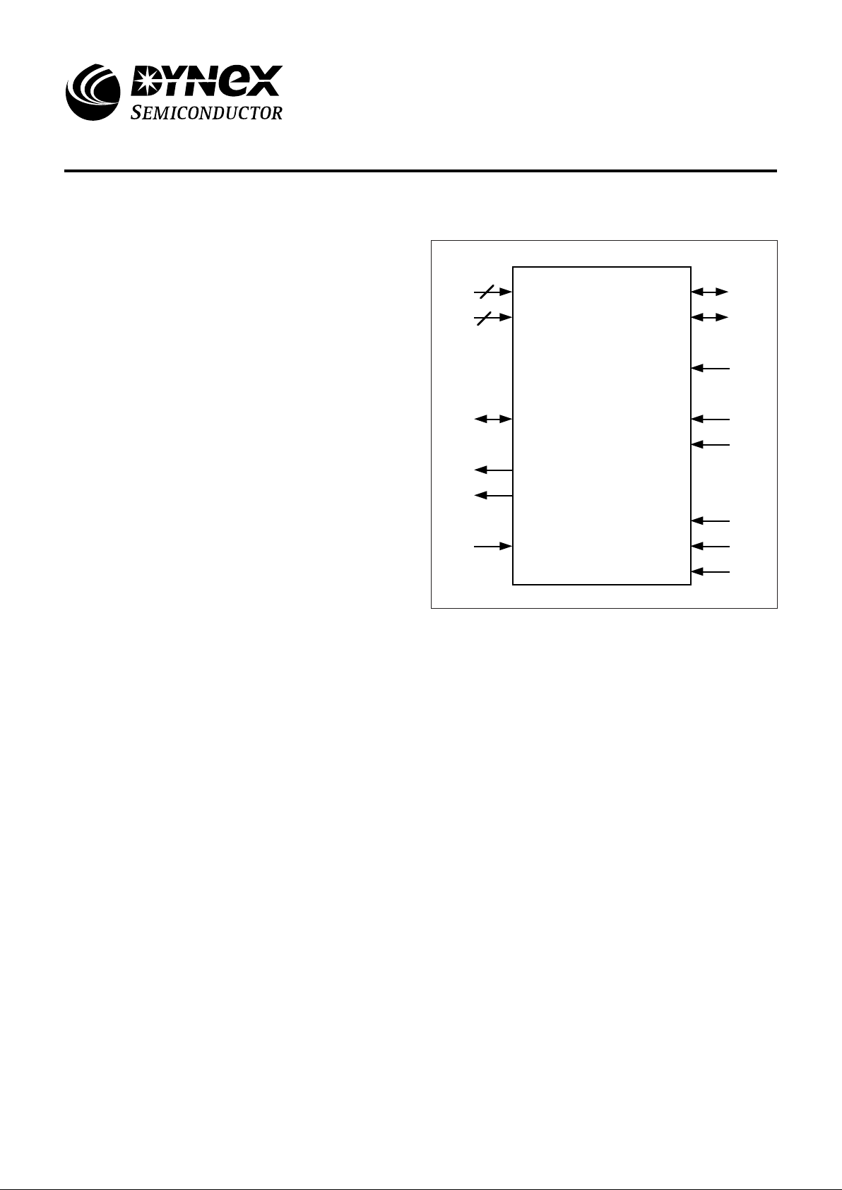
Figure 1: Chip Signals
FEATURES
■ Fast Feedthrough (35ns Detect and Correct Cycle)
■ 16-Bit Operation with 6 Check Bits
■ Radiation Hard CMOS/SOS Technology
■ Feedthrough Operation
■ Error Corrected/Uncorrected Flags
■ High Drive Capability on Memory Busses
VDD
VSS
PD[0:16]
CERRN
NCERRN
RDWN
MD[0:16]
CB[0:5]
XERRN
ENCOR
ENFLG
CS0
CS1N
CS2N
MA31755
EDAC
8
8
MA31755
16-Bit Feedthrough Error Detection
& Correction Unit (EDAC)
Replaces June 1999 version, DS3572-3.0 DS3572-4.0 January 2000

MA31755
2/13
1. PIN DESCRIPTIONS
POWER
BUSSES
ERROR FLAGS AND CONTROL
DEVICE AND BUFFER CONTROL
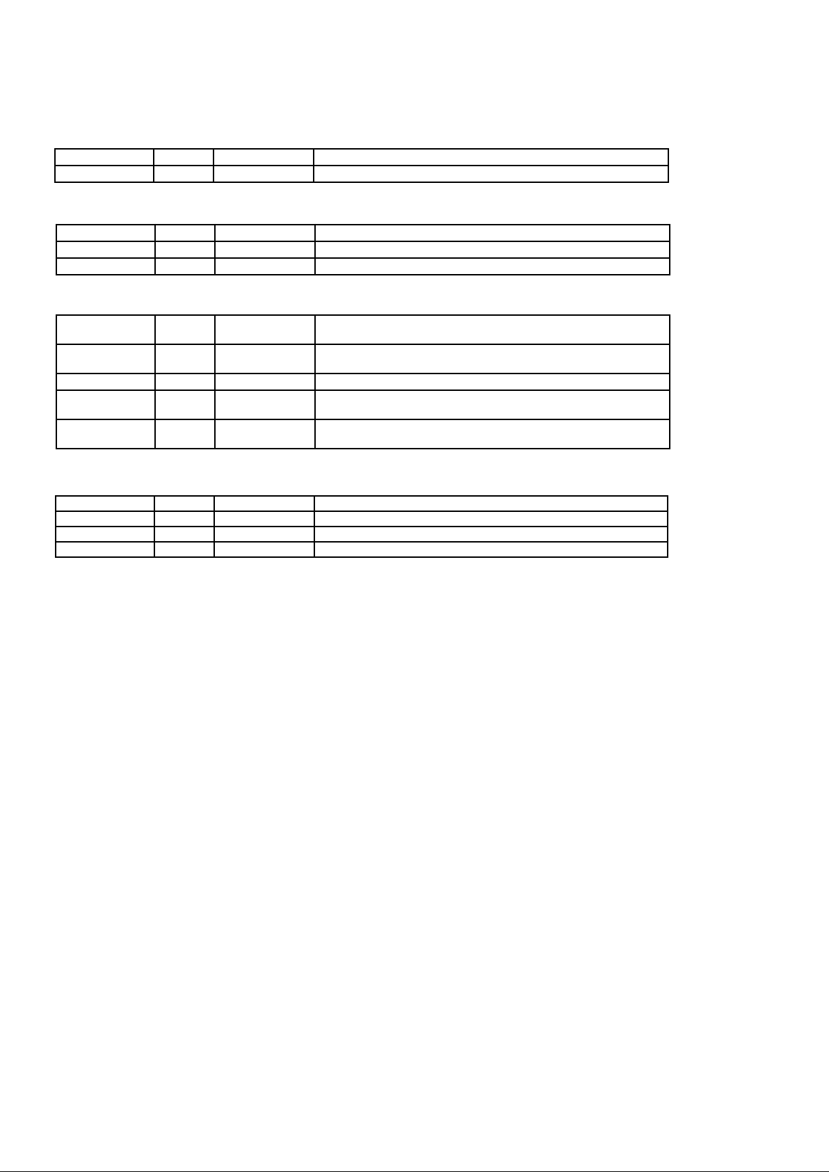
PD[0:16] I/O Active High Processor data bus + parity bit (bit 16)
MD[0:16] I/O Active High Memory data bus + parity bit (bit 16)
CB[0:5] I/O Active High Memory check bit bus
VDD x8 Input - Supply - 5V nominal (all must be connected)
VSS x8 Input - Circuit 0V reference (all must be connected)
CERRN Output Active Low Asserted low when a correctable (1 bit) error occurs (ENFLG
must be asserted high)
NCERRN Output Active Low Asserted low when an uncorrectable error occurs (ENFLG
must be asserted high)
XERRN Input Active Low External error feedthrough to NCERRN line.
ENCOR Input Active High Enables correction of data when high. Data is passed
through uncorrected when this line is low.
ENFLG Input Active High Enables the flagging of incorrect data when high. When this
line is low the two error flag lines are held inactive.
2. FUNCTIONAL DESCRIPTION
2.0 GENERAL
The EDAC is of feedthrough type with 16 data bits, 1 parity
bit and 6 check bits, giving the ability to correct all single bit
errors and detect all double bit errors. Errors in more than two
bits may result in any combination of error flags being raised
and the data may be arbitrarily modified by the correction
circuitry.
The EDAC is placed in the data bus between the processor
and the memory to be protected. It forms the interface
between the 23-bit memory bus and the 17-bit processor bus.
Tri-statable bus transceivers with a high drive capability are
incorporated at both busses.
2.1 TESTING THE EDAC AND MEMORY SYSTEM
No specific hardware for testing is provided by the
MA31755 since this would compromise the speed
performance of the part in normal operation. However, it is
possible to fully test the EDAC function and the generation of
the error signals without this. The system should provide a
means by which the check bit memory may be dynamically
write-enabled and disabled - this may be provided by gating
write strobe on the check bit memory with a latched control bit.
By writing first with check bits enabled, then with them
disabled, suitable seed values may be constructed which have
the required pattern of bits to test each feature of the EDAC
operation. A similar approach may be taken when testing the
check bit memory.
By disabling the EDAC (asserting ENCOR low) the
processor may have direct access to the unmodified 17-bit
data from the memory. Suitable test patterns may be applied to
test each memory location as required.
CS2N Input Active Low Enables device and output buffers.
CS1N Input Active Low Enables device and output buffers.
CS0 Input Active High Enables device and output buffers.
RDWN Input - High indicates a read cycle, low indicates a write cycle.

MA31755
3/13
2.2 BUS CONTROL
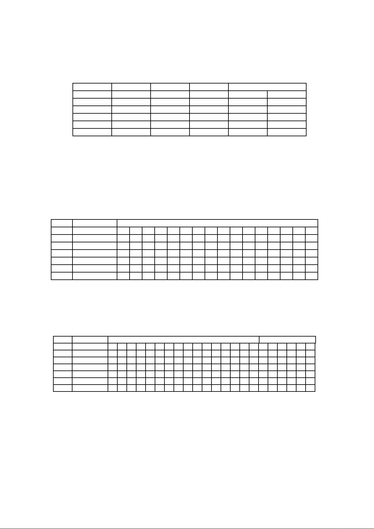
There are four signals which control the drive status of the EDAC external busses: RDWN, CS2N, CS1N and CS0. The
relationship to each other and to the EDAC busses is shown in Figure 2 below. The timing of these signals is shown in Figures 6
and 7.
Figure 2: Bus Control
2.3 INTERNAL OPERATION
2.3.1 Check Bit Generation
On write cycles the processor data word, PD[0:15], and the processor parity bit ,PD[16], are passed directly to the memory
data bus, MD[0:15], and the memory parity bit, MD[16].
The check bits, CB[0:5], are derived by 6 parity generators operating on sets of 8 bits of the processor data word, PD[0:15], as
shown in Figure 3 below:
Figure 3: Check Bit Generation
2.3.2 Syndrome Generation
The syndrome generation logic checks the sense of the check bits with respect to the memory data word. Six 9-input parity
checkers generate the syndrome bits, SY[0:5], according to figure 4 below:
Figure 4: Syndrome Generation
RDWN CS2N CS1N CS0 Bus state
Processor Memory
X High X X Tristate Tristate
X X High X Tristate Tristate
X X X Low Tristate Tristate
High Low Low High Output Input
Low Low Low High Input Output
CB Parity PD
15 14 13 12 11 10 9 8 7 6 5 4 3 2 1 0
0 Even X X X X X X X X
1 Even X X X X X X X X
2 Odd X X X X X X X X
3 Odd X X X X X X X X
4 Even X X X X X X X X
5 Even X X X X X X X X
If there are no errors in the memory data word, MD[0:15],
or the check bits, CB[0:5], then all of the syndrome bits,
SY[0:5], will be set low.
A single bit error in the memory data word, MD[0:15], will
cause 3 syndrome bits to be set high. However, a single bit
error in the check bits, CB[0:5], will cause only 1 syndrome bit
to be set high. A two bit error in the memory data word and/or
the check bits will cause either 2, 4, 5 or 6 syndrome bits to be
set.
Three or more errors in the memory data word and/or the
check bits will cause an undefined number of syndrome bits to
be set. This will cause the operation of the device in respect of
the states of CERRN, NCERRN and data on the PD bus to be
unpredictable.
S Y Parity MD CB
1514131211109876543210012345
0 Even X X XXXXX XX
1 Even X XXXX X X X X
2 Odd X X X X XXXX X
3 Odd X X X XXXXX X
4 Even X XXXXX X X X
5 Even XXXXX XX X X

MA31755
4/13
2.3.3 Correction
With no syndrome bits set data will pass through from the
MD bus to the PD bus unchanged. When a single bit error
occurs in the memory data word, MD[0:15], the three
syndrome bits which are set identify which data bit is in error.
The correction logic decodes these syndrome bits and will
correct the error provided the correction enable input, ENCOR,
is high.
2.3.4 Flag Generation
The correctable error flag,CERRN, is driven low whenever
1 or 3 syndrome bits are set and flags are enabled (ENFLG=1).
The non-correctable error flag, NCERRN, is driven low
whenever 2, 4, 5 or 6 Syndrome bits are set and flags are
again enabled (ENFLG=1). NCERRN will also be driven low
should the external error input, XERRN, be driven low at any
time. Note: this external error feedthrough from XERRN to
NCERRN operates independently of ENFLG and the Chip
Select inputs (CS0, CS1N & CS2N).
Flags are enabled provided the ENFLG input is high and
the device is selected. Note: the flags are not disabled on write
cycles and therefore can indicate errors on write operations
caused by faults on the Memory Data Bus and the Check Bit
Bus.
2.3.5 Internal Structure
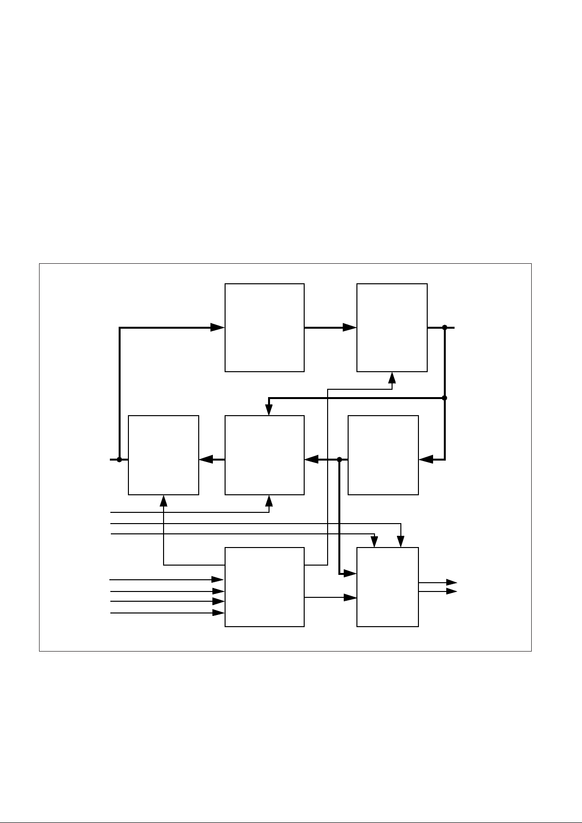
Figure 5 below shows the internal block diagram
representing the internal architecture of the MA31755.
Figure 5: Block Diagram of the Internal Architecture of the MA31755
Check bit
generation
Tri-statable
Buffer
Tri-statable
Buffer
Correction
Syndrome
Generation
MD[0:16]
CB[0:5]
CERRN
NCERRN
PD[0:16]
ENCOR
ENFLG
XERRN
RDWN
CS0
CS1N
CS2N
Buffer
Control
Flags
Generation
 Loading...