DYNEX DGT409BCA Datasheet

DGT409BCA
DGT409BCA
Reverse Blocking Gate Turn-off Thyristor
Replaces January 2000 version, DS4414-4.0 DS4414-4.1 February 2002
APPLICATIONS
The DGT409 BCA is a symmetrical GTO designed for
applications which specifically require a reverse blocking
capability, such as current source inverters (CSI). Reverse
recovery ratings and characteristics are included.
FEATURES
■ Reverse Blocking Capability
■ Double Side Cooling
■ High Reliability In Service
■ High Voltage Capability
■ Fault Protection Without Fuses
■ Turn-off Capability Allows Reduction In Equipment Size
And Weight. Low Noise Emission Reduces Acoustic
Cladding Necessary For Environmental Requirements
ORDERING INFORMATION
Order as: DGT409BCA6565
KEY PARAMETERS
I
TCM
V
DRM/VDRM
dV
/dt 1000V/µs
D
di
/dt 300A/µs
T
1500A
6500V
Outline type code: CA
See Package Details for further information
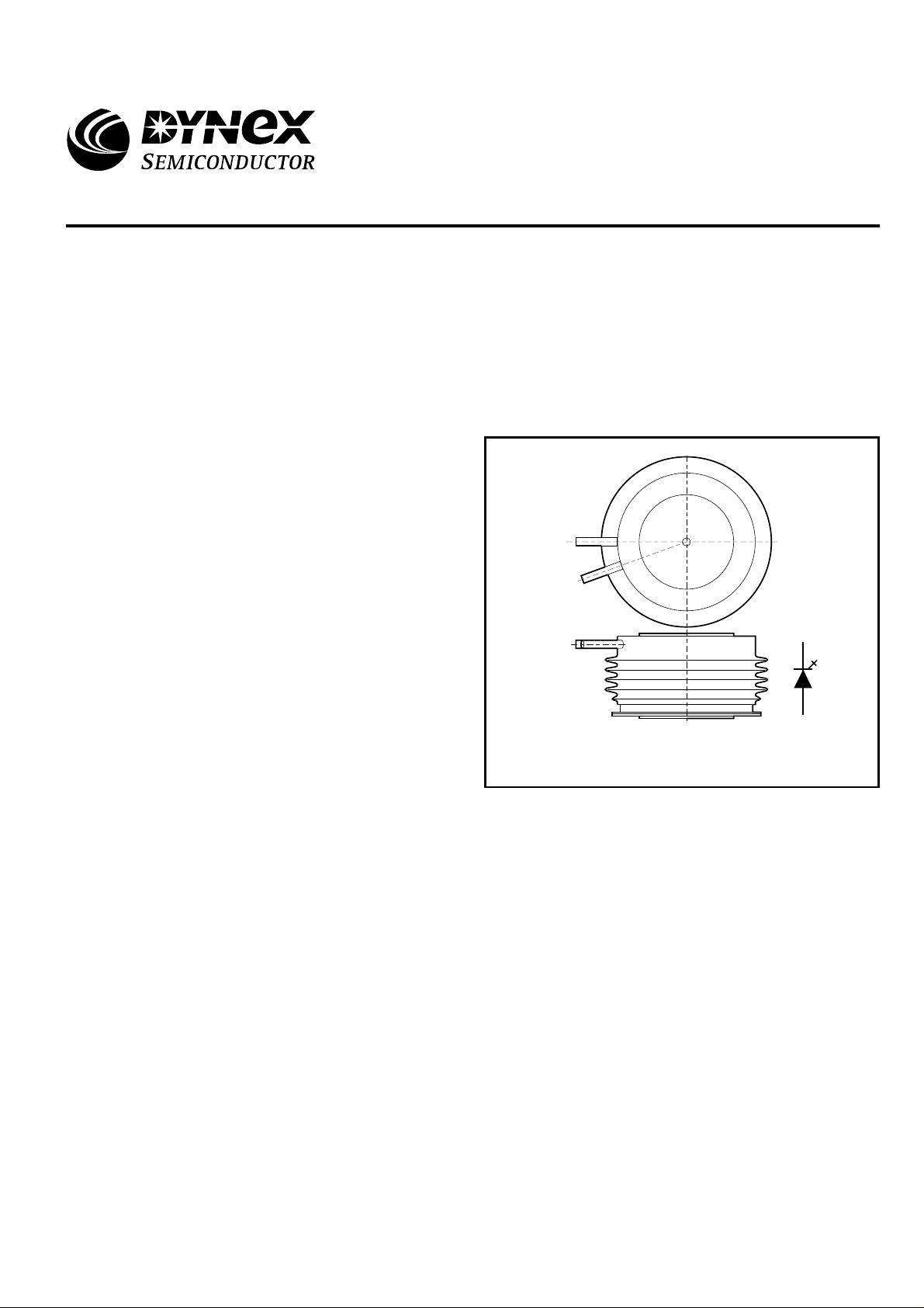
Fig. 1 Package outline
1/11

DGT409BCA
ABSOLUTE MAXIMUM RATINGS
Stresses above those listed under 'Absolute Maximum Ratings' may cause permanent damage to the device. This is a stress rating
only and functional operation of the device at these or any other conditions above those indicated in the operational sections of this
specification is not implied. Exposure to Absolute Maximum Ratings for extended periods may affect device reliability.
Tj = 115˚C unless staed otherwise
Symbol Parameter Conditions Max.
V
DRM
V
RRM
I
TCM
I
TSM
I2t
/dt
di
T
Repetitive peak off-state voltage
Surge (non-repetitive) on-state current
I2t for fusing
Critical rate of rise of on-state current 300
IDM = 100mA V6500
I
= 100mA V6500Repetitive peak reverse voltage
RRM
VD = 4300V, diGQ/dt = 20A/µs, CS = 2.0µFA1500Repetitive peak controllable on-state current
10ms half sine.
10ms half sine.
= 3000V, IT = 800A, IFG > 20A, tr > 1.5µsA/µs
V
D
VD = 3000V, RGK ≤ 1.5Ω
dVD/dt
L
Rate of rise of off-state voltage
V
= 3000V, VRG = –2V
D
I
Peak stray inductance in snubber circuit 200 nH
S
= 1500A, VDM = 6000V, dIGQ/dt = 20A/µs, CS = 2µF
T
GATE RATINGS
Symbol Parameter Conditions
Min.
Units
3
3
45 x 10
175 V/µs
1000 V/µs
kA
2
A
s
UnitsMax.
V
RGM
I
FGM
P
FG(AV)
P
RGM
diGQ/dt
t
ON(min)
t
OFF(min)
RGM
Peak forward gate current
Average forward gate power
Peak reverse gate power
Rate of rise of reverse gate current
Minimum permissable on time
Minimum permissable off time
Continuous reverse gate-cathode current 50 mA-I
This value may be exceeded during turn-off
-
-
-
-
-
-
V
= 16V, No gate cathode resistor
RGM
20
15
-Peak reverse gate voltage
25
70
10
-
15
-
60
-50
V
A
W
kW
A/µs
µs
- µs150
2/11

THERMAL RATINGS AND MECHANICAL DATA
DGT409BCA
Symbol Parameter Conditions Max.Min.
Double side cooled
R
th(j-hs)
DC thermal resistance - junction to heatsink
surface
Anode side cooled
Cathode side cooled
R
th(c-hs)
T
T
OP/Tstg
Contact thermal resistance
Virtual junction temperature
vj
Clamping force 12.0kN
With mounting compound
Operating junction/storage temperature range
-
Clamping force
per contact
CHARACTERISTICS
Tj = 115oC unless stated otherwise
Symbol Parameter
TM
On-state voltageV
At 200A peak, I
Conditions
= 4A d.c.
G(ON)
Units
- 0.046oC/W
-
- 0.124
- 0.009
-
-40
11.0
115
115
15.0
o
C/W0.073
o
C/W
o
C/W
o
o
kN
C
C
Min. Max. Units
-4V
I
E
Q
I
RRM
V
I
I
RGM
E
t
t
t
DM
GT
GT
ON
t
d
t
OFF
gs
gf
gq
GQ
Peak off-state current
Peak reverse current
Gate trigger voltage
Gate trigger current
Reverse gate cathode current
Turn-on energy
Delay time
Rise time
r
Turn-off energy
Storage time
Fall time
Gate controlled turn-off time
Turn-off gate charge
V
= 6500V, VRG = 0V - 100 mA
DRM
At V
= 6500V - 100 mA
RRM
VD = 24V, IT = 100A, Tj = 25oC-1V
VD = 24V, IT = 100A, Tj = 25oC-2A
V
= 16V, No gate/cathode resistor
RGM
VD = 3000V
IT = 400A, dIT/dt = 150A/µs
IFG = 20A, tr < 1.5µs
50-
-7µs
mA
mJ2500-
µs3-
- 2500 mJ
µs
µs
µs
µC
I
= 800A, VDM = 3000V
T
Snubber Cap CS = 2µF,
diGQ/dt = 20A/µs
See Figs. 16 and 17
See Figs. 16 and 17
See Figs. 16 and 17
- 3600
Q
I
GQT
GQM
Total turn-off gate charge
Peak reverse gate current
- 7200 µC
- 350 A
3/11

DGT409BCA
0.9x V
D
0.9x I
T
dVD/dt
D
V
T
I
V
DM
V
D
Anode voltage and current
0.1x V
D
t
t
d
r
t
gt
I
dIFG/dt
0.1x I
FG
FG
V
FG
t
w1
0.1x I
0.5x I
Gate voltage and current
Recommended gate conditions to switch off I
I
= 30A
FG
I
= 4A d.c.
G(ON)
t
= 20µs
w1(min)
I
= 270A typical
GQM
di
/dt = 30A/µs
GQ
Q
= 2200µC
GQ
V
= 2V
RG(min)
V
= 15V
RG(max)
GQ
GQM
I
GQM
Q
GQ
= 800A:
TCM
I
DP
V
t
gs
t
gf
t
gq
I
G(ON)
TAIL
V
(RG)BR
RG
V
4/11
These are recommended Dynex Semiconductor conditions. Other conditions are permitted
according to users gate drive specifications.
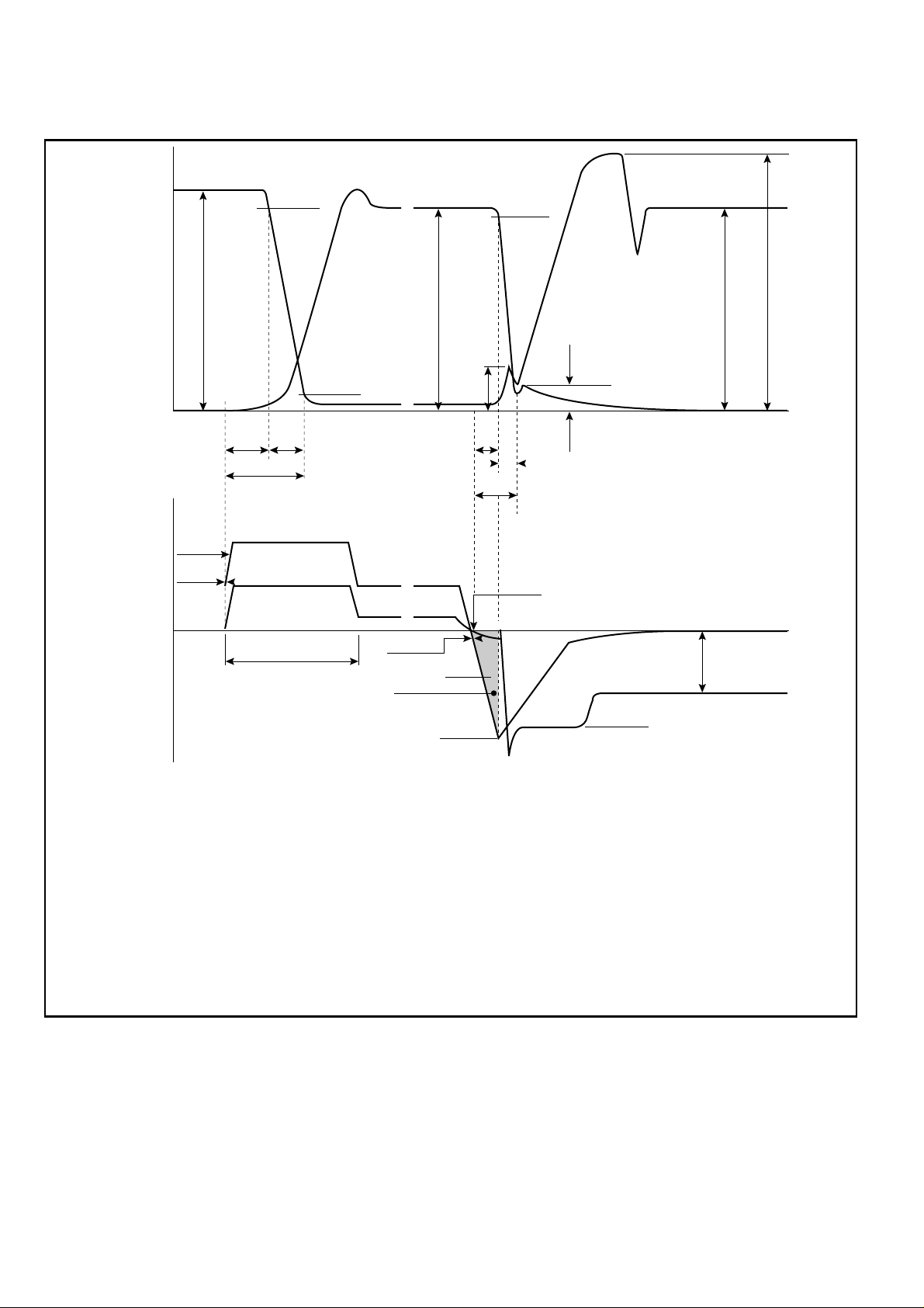
Fig.2 General switching waveforms
 Loading...