DYNEX DGT304SE13 Datasheet

DGT304SE13
DGT304SE
Gate Turn-off Thyristor
Replaces January 2000 version, DS4609-4.0 DS4609-4.1 February 2002
APPLICATIONS
■ Variable speed A.C. motor drive inverters (VSD-AC)
■ Uninterruptable Power Supplies
■ High Voltage Converters
■ Choppers
■ Welding
■ Induction Heating
■ DC/DC Converters
FEATURES
■ Double Side Cooling
■ High Reliability In Service
■ High Voltage Capability
■ Fault Protection Without Fuses
■ High Surge Current Capability
■ Turn-off Capability Allows Reduction In Equipment
Size And Weight. Low Noise Emission Reduces Acoustic
Cladding Necessary For Environmental Requirements
KEY PARAMETERS
I
TCM
V
DRM
I
T(AV)
dV
/dt 500V/µs
D
di
/dt 500A/µs
T
700A
1300V
250A
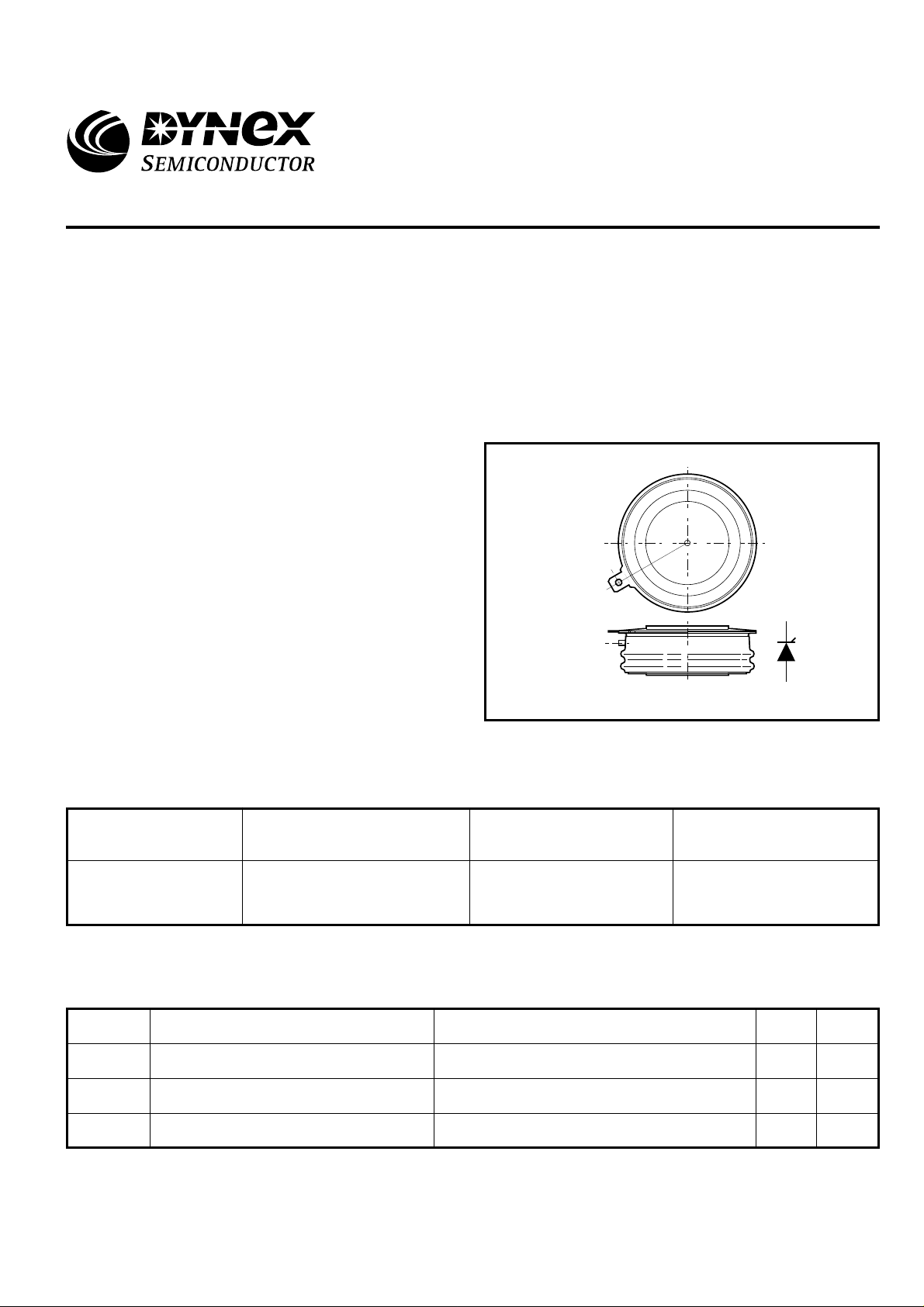
Outline type code: E.
See Package Details for further information.
VOLTAGE RATINGS
Repetitive Peak Off-state Voltage
V
DRM
V
1300DGT304SE13
Repetitive Peak Reverse Voltage
V
RRM
V
16
ConditionsType Number
= 125oC, IDM = 50mA,
T
vj
= 50mA, VRG = 2V
I
RRM
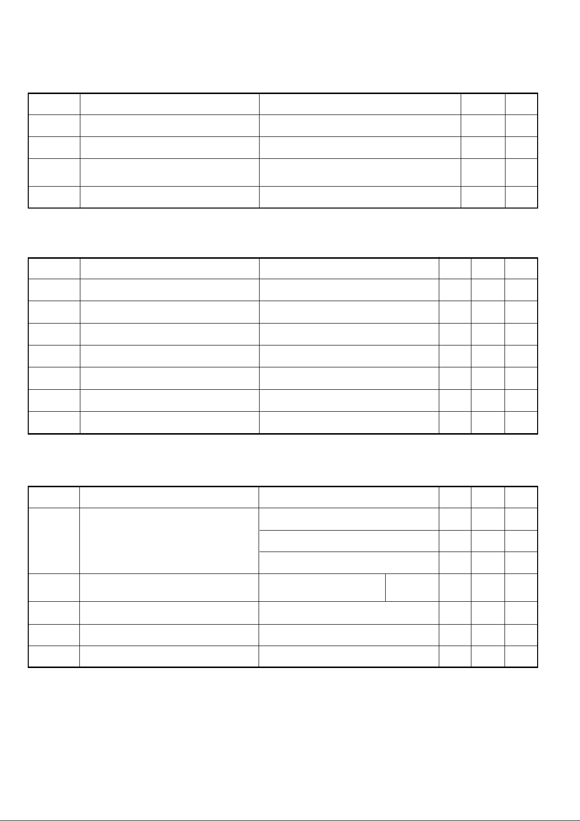
CURRENT RATINGS
Symbol Parameter Conditions Max.
I
TCM
I
T(AV)
I
T(RMS)
Repetitive peak controllable on-state current
Mean on-state current
RMS on-state current A
V
= 60%V
D
THS = 80oC. Double side cooled. Half sine 50Hz.
THS = 80oC. Double side cooled. Half sine 50Hz.
, Tj = 125oC, diGQ/dt =15A/µs, Cs = 2.0µF
DRM
250
390
Units
A700
A
1/13

DGT304SE13
SURGE RATINGS
Symbol Parameter
I
TSM
I2t
diT/dt Critical rate of rise of on-state current 500
dVD/dt
Surge (non-repetitive) on-state current
I2t for fusing
Rate of rise of off-state voltage
10ms half sine. Tj = 125oC
10ms half sine. Tj =125oC
VD = 60% V
Rise time < 1.0µs
To 80% V
DRM
Conditions
, IT = 700A, Tj = 125oC, IFG > 20A,
DRM
; RGK ≤ 1.5Ω, Tj = 125oC
GATE RATINGS
Symbol Parameter Conditions
V
RGM
I
FGM
P
FG(AV)
P
RGM
diGQ/dt
Peak forward gate current
Average forward gate power
Peak reverse gate power
Rate of rise of reverse gate current
This value maybe exceeded during turn-off
Min.
Max. Units
4.0
80000
500 V/µs
-Peak reverse gate voltage
-
-
-
10
16
50
10
50
kA
2
s
A
A/µs
UnitsMax.
V
A
W
6
kW
A/µs
t
ON(min)
t
OFF(min)
Minimum permissable on time
Minimum permissable off time
THERMAL RATINGS
Symbol Parameter Conditions Max.Min.
Double side cooled
R
R
th(c-hs)
T
T
OP/Tstg
th(j-hs)
vj
-
DC thermal resistance - junction to heatsink
surface
Contact thermal resistance
Virtual junction temperature
Operating junction/storage temperature range
Clamping force
Anode side cooled
Cathode side cooled
Clamping force 5.5kN
With mounting compound
per contact
-20
- µs40
Units
- 0.075oC/W
-
- 0.20
- 0.018
-
-40
5.0
125
125
6.0
o
o
o
µs
C/W0.12
C/W
C/W
o
C
o
C
kN
2/13

CHARACTERISTICS
= 125oC unless stated otherwise
T
j
DGT304SE13
Symbol Parameter
On-state voltageV
Peak off-state current
Peak reverse current
Gate trigger voltage
Gate trigger current
Reverse gate cathode current
Turn-on energy
Delay time
Rise time
r
Turn-off energy
Storage time
Fall time
I
I
E
E
I
RRM
V
I
RGM
t
t
DM
GT
t
t
OFF
gs
gf
TM
GT
ON
d
Min. Max. Units
- 2.2 V
-50mA
At 600A peak, I
At = V
At V
, VRG = 2V - 25 mA
DRM
RRM
Conditions
= 2A d.c.
G(ON)
VD = 24V, IT = 100A, Tj = 25oC - 0.9 V
= 24V, IT = 100A, Tj = 25oC - 1.0 A
V
D
V
= 16V, No gate/cathode resistor
RGM
= 900V, IT = 600A, dIT/dt = 300A/µs
D
50-
mA
mJ130-V
IFG = 20A, rise time < 1.0µs
RL = (Residual inductance 3µH)
- 3.0 µs
- 350 mJ
=600A, VDM = 750V
I
T
-10µs
Snubber Cap Cs = 1.5µF,
µs1.5-
µs11-
t
gq
Q
GQ
Q
GQT
Gate controlled turn-off time
Turn-off gate charge
Total turn-off gate charge
diGQ/dt = 15A/µs
RL = (Residual inductance 3µH)
- 700
- 1400 µC
µs0.9-
µC
3/13

DGT304SE13
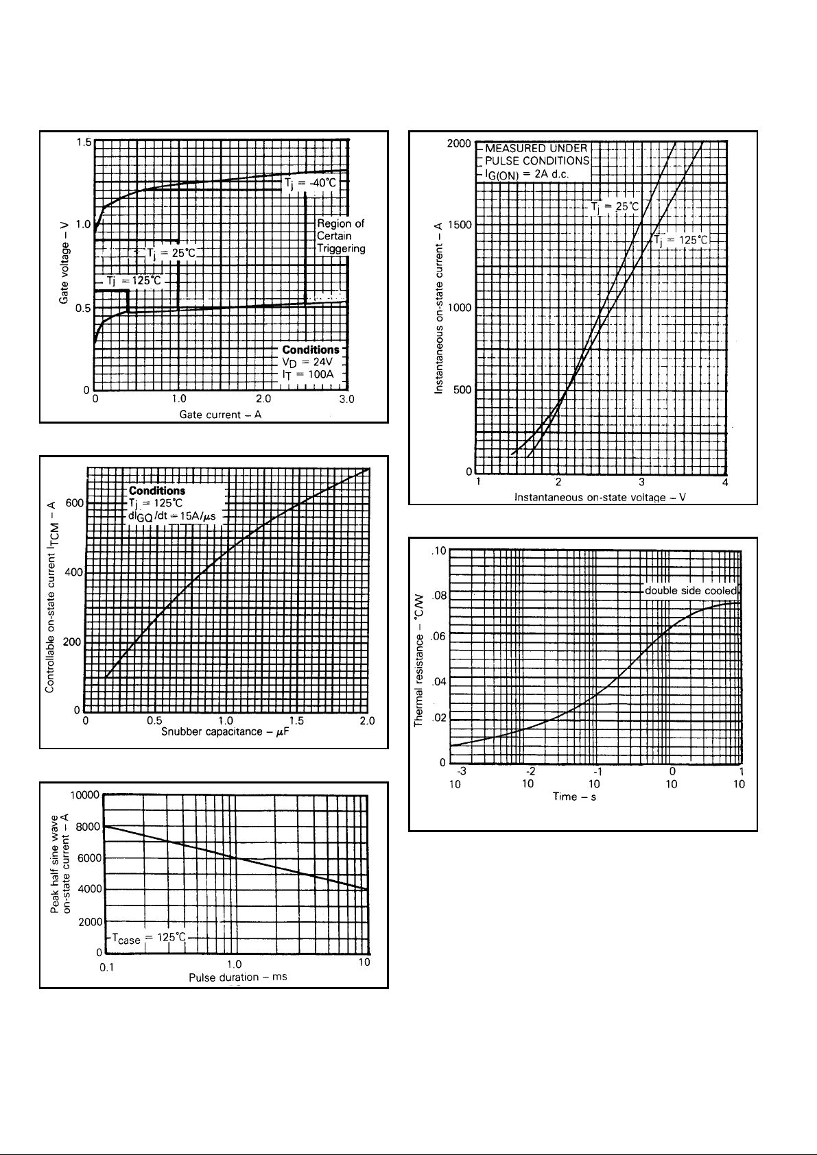
CURVES
Fig.1 Gate characteristics
Fig.3 Dependence of I
TCM
on C
Fig.2 Maximum (limit) on-state characteristics
S
Fig.4 Maximum (limit) transient thermal resistance
Fig.5 Surge (non-repetitive) on-state current vs time
4/13
 Loading...