DYNEX DF451 User Manual

DF451
DF451
Fast Recovery Diode
Replaces January 2000 version, DS4142-5.0 DS4143-6.0 June 2004
FEATURES
■ Double Side Cooling
■ High Surge Capability
■ Low Recovery Charge
APPLICATIONS
■ Induction Heating
■ A.C. Motor Drives
■ Inverters And Choppers
■ Welding
■ High Frequency Rectification
■ UPS
VOLTAGE RATINGS
Type Number Repetitive Peak
Reverse Voltage
V
RRM
V
DF451 16
DF451 14
DF451 12
DF451 10
DF451 08
DF451 06
1600
1400
1200
1000
800
600
Conditions
V
= V
RSM
RRM
+ 100V
KEY PARAMETERS
V
RRM
I
F(AV)
I
FSM
Q
r
t
rr
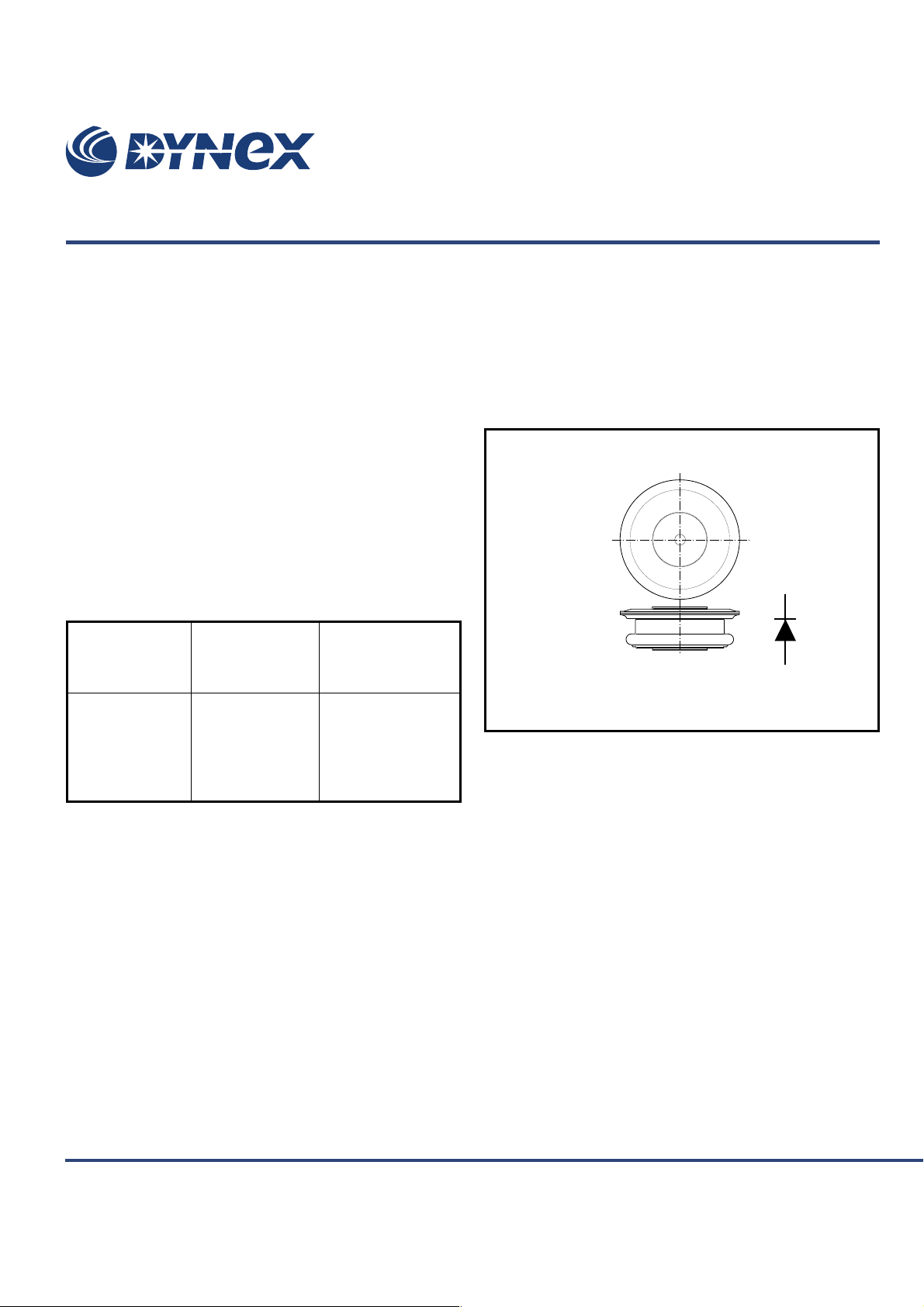
Outline type code: M771.
See Package Details for further information.
Fig. 1 Package outline
1600V
295A
3500A
25µC
1.22µs
ORDERING INFORMATION
When ordering, select the required part number shown in the
Voltage Ratings selection table, e.g.:
DF451 12
Note: Please use the complete part number when ordering and
quote this number in any future correspondance relating to your
order.
www.dynexsemi.com
1/7

DF451
CURRENT RATINGS
Symbol Parameter Conditions
Double Side Cooled
I
F(AV)
I
F(RMS)
Mean forward current
RMS value
I
F
Continuous (direct) forward current
Half wave resistive load, T
T
= 65oC 543 A
case
T
= 65oC 391 A
case
Single Side Cooled (Anode side)
I
F(AV)
I
F(RMS)
I
F
Mean forward current
RMS value
Continuous (direct) forward current
Half wave resistive load, T
= 65oC 348 A
T
case
T
= 65oC 285 A
case
SURGE RATINGS
Conditions
FSM
ParameterSymbol
Surge (non-repetitive) forward currentI
10ms half sine; with 0% V
= 65oC 295 A
case
= 65oC 220 A
case
Max. Units
3.5 kA
= 150oC
RRM, Tj
61.25 x 10³A2sI2t for fusingI2t
UnitsMax.
FSM
Surge (non-repetitive) forward currentI
THERMAL AND MECHANICAL DATA
Symbol
R
th(j-c)
R
th(c-h)
T
vj
T
stg
Thermal resistance - junction to case
Thermal resistance - case to heatsink
Virtual junction temperature
Storage temperature range
Parameter
2.8 kA
10ms half sine; with 50% V
RRM, Tj
= 150oC
39.2 x 10
Conditions Max. Units
Double side cooled
dc
-
-0.07
Anode dc
Single side cooled
Cathode dc
Clamping force 5.0kN
with mounting compound
Forward (conducting) - 150
Double side
Single side
- 0.147oC/W
0.02
-
-0.02
–55 150
5.54.5Clamping force-
3
A2sI2t for fusingI2t
o
C/W
o
C/W- 0.133
o
C/W
o
C/W
o
C
o
C
kN
2/7
www.dynexsemi.com

CHARACTERISTICS
DF451
Symbol Typ. Units
V
FM
I
RRM
t
rr
Q
RA1
I
RM
K
V
TO
r
T
V
FRM
Forward voltage
Peak reverse current
Reverse recovery time
Recovered charge (50% chord)
Reverse recovery current
Soft factor
Threshold voltage
Slope resistance
Forward recovery voltage di/dt = 1000A/µs, T
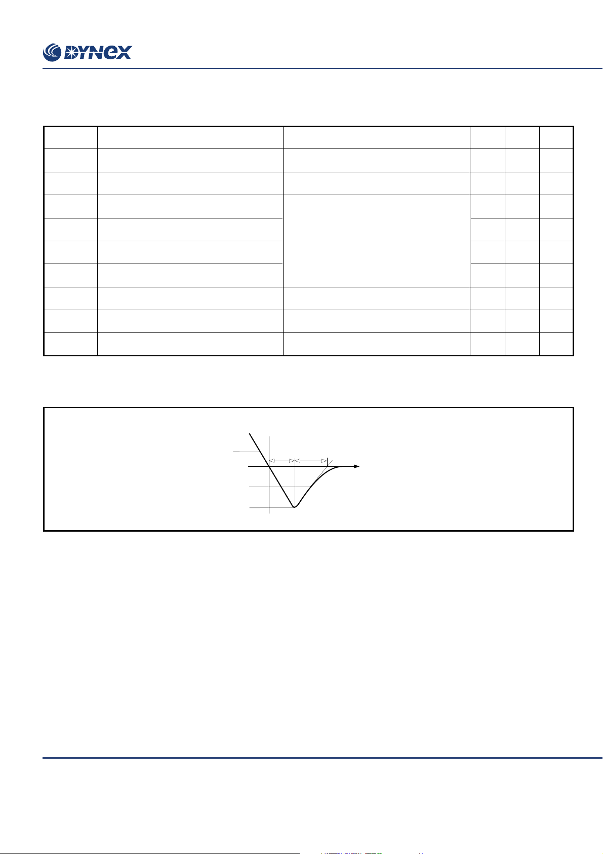
DEFINITION OF K FACTOR AND Q
Parameter
RA1
Conditions Max.
At 600A peak, T
At V
, T
RRM
case
I
= 500A, di
F
T
= 125oC, VR = 100V
case
= 25oC - 2.65 V
case
= 125oC-mA
1.22
/dt = -80A/µs
RR
100
-
-25µC
-40A
1.7 - -
At Tvj = 125oC-1.6V
o
= 125
At T
vj
C-1.5mΩ
= 125oC-40V
j
Q
= 0.5x IRR(t1 + t2)
RA1
µs
dIR/dt
0.5x I
k = t
t
t
1
2
RR
I
RR
1/t2
τ
www.dynexsemi.com
3/7
 Loading...