

Page 1
I
T
I
T(AV)
V
TM
V
TO
r
T
3x I
T(AV)
查询DCR1675SA供应商
AN5001 Application Note
AN5001
Use Of The VTO, rT On-state Characteristic Model
Application Note
Replaces February 2003 version, AN5001-6.0 AN5001-7.0 February 2004
The use of the VTO, rT on-state characteristic model and a
more accurate alternative.
The inclusion of the theoretical terms V
and rT in power
TO
semiconductor data sheets allows a simple means of calculating
power loss, but this can lead to many incorrect assumptions.
The terms in question are the two coefficients of a simple straight
line model of the device on-state characteristic curve. To
calculate the power the following formula is used:
P = V
T0 IT(AV)
+ rT k2 I
T(AV)
2
[1]
where k is the current waveform form factor, eg 1.57 for half
sine wave.
The use of V
and rT to approximate to the forward volt drop
TO
curve of a power semiconductor originates from pre-computer
days when engineers used slide rules, calculators and, later
on, simple computers for their calculations. The use of modern
computers means that better approximations to the characteristic
can easily be used. The most popular of these is the model
proposed by General Electric:
= A + B*lnI + C*I + D*sqrt(I) [2]
V
TM
where A, B, C and D are constants with values specific to the
device in question.
The use of this model is described below.
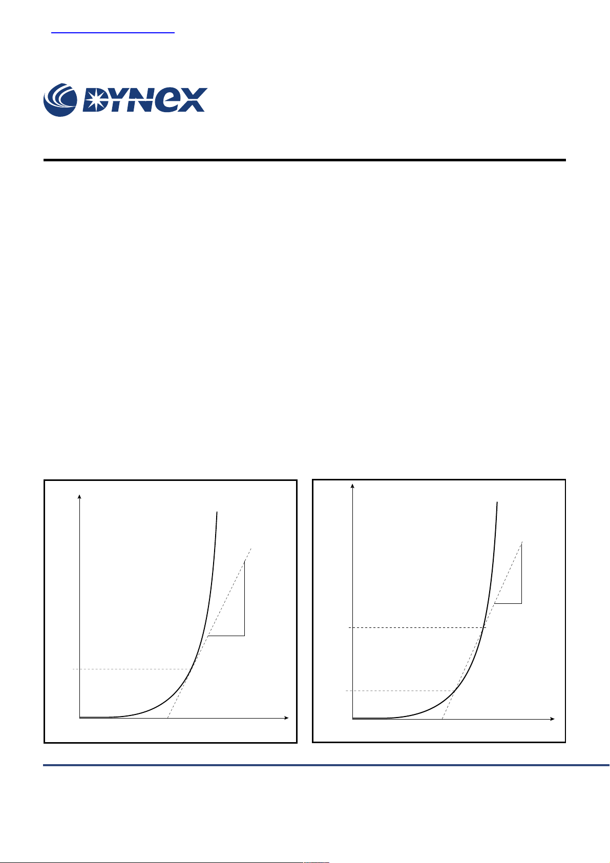
VT0, rT DEFINITIONS
Although the straight line model is basically simple, variations in
definition can lead to significant differences in calculated powers.
Different manufacturers of power semiconductors have defined
V
and rT in different ways. Here are 4 variations:
T0
1) As fig. 1, where the line is the tangent to the V
at the average current.
2) As fig. 2, where a chord is drawn through I
This variation is the one used by Dynex for the calculation of
data sheet power losses and current ratings. The definition
is commonly used for thyristors. For rectifier diodes a chord
through 3xI
T(AV)
and 5xI
sometimes gives a better result.
T(AV)
3) A variation of 2 which uses two straight lines instead of one
to approximate to the true curve. In this version the lines
TM
T(AV)
vs IT curve
and 3xI
T(AV)
.
I
T
I
T(AV)
www.dynexsemi.com
V
TO
Fig.1
r
T
V
T
Fig.2
1/5
Page 2
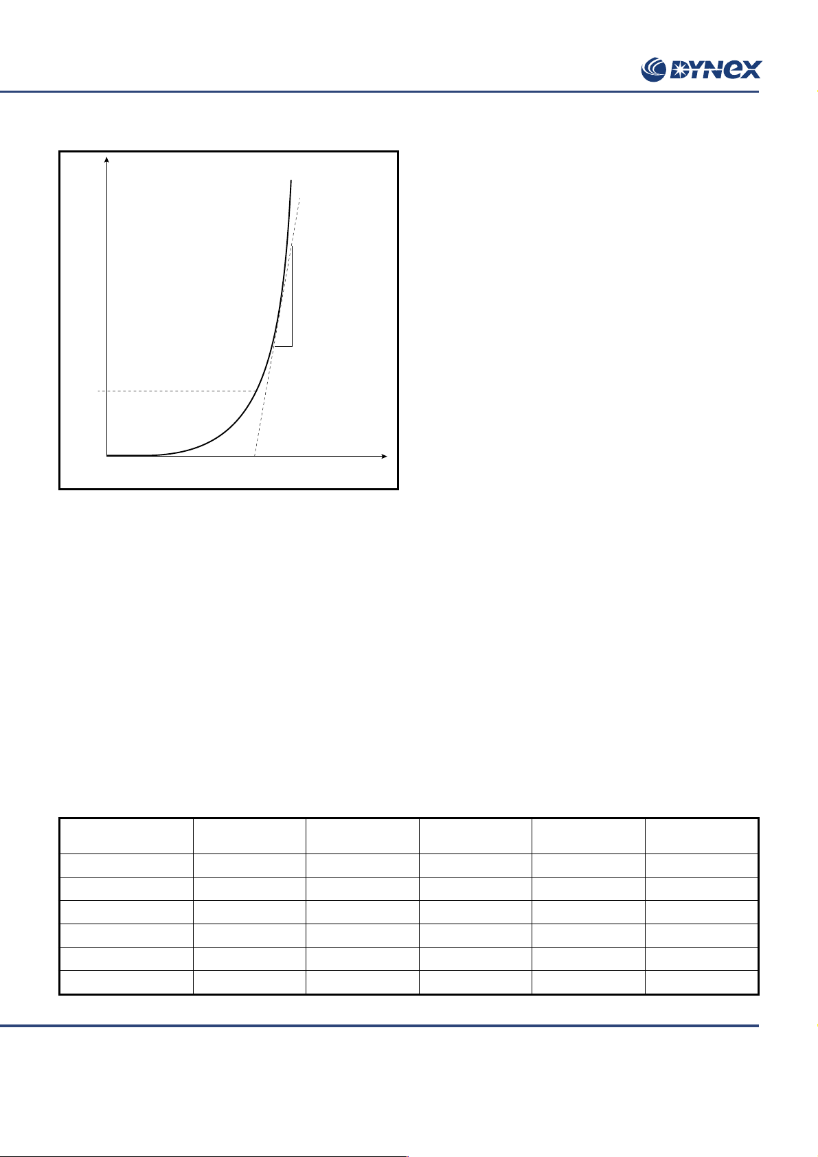
AN5001 Application Note
I
T
r
T
I
T(AV)
V
TO
V
T
Fig.3
pass through 1/6I
T(AV)
and πI
and also πI
T(AV)
and 20 x I
T(AV)
T(AV)
4) As Fig 3. A tangential point constructed such that the value
calculated from:-
of I
T(AV)
I
T(AV)
= (–V
± ÷ (V
TO
2
+ 4*k2*rT*P)) / 2*k2*r
TO
T
[3]
is the same as that calculated by more exacting methods. This
method is a variation of method 1). It has been used to
retrospectively calculate meaningful values of V
and rT where
T0
more accurate current rating data already exists.
and 4 give adequate accuracy up to 3 x I
T(AV)
.
For improved accuracy a mathematical model is needed which
approximates better to the true curve.
A FOUR COEFFICIENT MODEL
The GE four term curve-fit equation given above has been
shown to be a good isothermal approximation and is being
increasingly adopted by several manufacturers of power
semiconductors for inclusion in their datasheets. For the user,
the one problem with the equation
= A + B*lnI + C*I + D*sqrt(I) [4]
V
TM
is that, when multiplied by the equation for the current, it is not
easily integratable to give the power loss. However, the equation
is solvable by numerical integration, now easily possible with
computers.
The following equation for half sine waves uses the A, B, C, D
coefficients used in the V
equation above, their numerical
TM
values depending on the device type.
2
P = [(A*(I/E) + B*(I/E)* ln(I/E))*F + B*(I/E)*G + C*(I/E)
*H+ D*(I/E)
.
where I is the peak value of the half sine wave current.
The values of E, F, G, H and J depend on the conduction angle
and are given in the table 1, and for Rectangular waves :
P = [ A + B*ln(I*360/θ) + C*(I*360/θ) + D*÷(I*360/θ) ]*(I*360/θ)]
where I is the average current
(not the peak current)
the conduction angle in degrees.
3/2
*J]
[5]
[6]
and θ is
LIMITATIONS OF THE V
T0, RT
MODEL
Using any one of the four definitions gives the correct value of
the conduction losses at one or at most two points on the V
TM
vs IT curve, ie where the straight line meets the true curve. It can
be seen that depending on where a point is taken on the curve
the answers will be optimistic or pessimistic. Definitions 1, 2
elgnAnoitcudnoC
)seerged(
EFGHJ
0811 68903813.00626790.0–52.026802872.0
0211 05325732.07042250.0–59700020.002797512.0
0957.009167751.08218840.0–00116321.003517731.0
0654.012877080.09483540.0–63029940.003114260.0
0352.027726020.05065420.0–88468600.021966110.0
51760.064360500.03905900.0–79748000.033130200.0
Table 1
2/5
Dynex Semiconductor has determined the values of A, B, C and
D and these are given in the attached table 2.
www.dynexsemi.com
Page 3

AN5001 Application Note
rebmuNepyTeciveDABCD
TS405RCD473153.0418171.0469000.0616020.0–
ES406RCD155680.1130371.0– 01x164703.3–
E027RCD6632.02811.05000.09100.0–
GS308RCD302464.0615150.0942000.0159500.0
GS608RCD9262016.030294080.001x730981.7
GS818RCD640056.0126810.0– 985000.0106360.0
GS028RCD577957.0– 522936.0673400.0351290.0–
F048RCD464085896.6637301175.1– 868012100.0– 759849932.0
FS2001RCD5746.0– 9703.07872000.011320.0–
FS3001RCD752191.1– 4879414.001x888326.3
FS6001RCD269654.1– 9731635.001x949936.6
FS8001RCD574854.1553890.0– 484000.0565210.0
5–
4–
4–
4–
543650.0
82382010.0–
75219920.0–
58550940.0–
FS0201RCD36852.0985223.0465200.0950160.0–
FS1201RCD6213.0– 4472.0100.03410.0–
F0501RCD574854.1553890.0– 484000.0565210.0
ABS4731RCD3456484.048980450.001x620805.8
ABS5731RCD689941.193909990.0– 01x895399.7
ABS6731RCD301954.116530570.0– 01x776244.3
VS4741RCD/YS4741RCD5035367.001x63037.8
3–
5–
5–
4–
5–
01x753865.8
VS5741RCD/YS5741RCD6455099.0861152440.0– 67911000.0153521900.0
VS6741RCD/YS6741RCD1469568.069489630.001x983542.3
VS6741RCD/YS4751RCD499823.11361831.0– 01x379565.3
VS6741RCD/YS5751RCD746956.19946022.0– 01x799724.7
4–
6–
5–
VS6741RCD/YS6751RCD388276414.0269421930.0770882000.0836415800.0
A0895RCD4264.05720.001x1052.2
WS4951RCD851251.182410480.0– 01x450153.3
WS5951RCD15666820.03930951.001x485749.1
WS6951RCD9551105.0– 7148362.001x4117635.2
AS3761RCD/ZS3761RCD5350816.0569700.001x75.4
AS4761RCD/ZS4761RCD2494486.05468010.0– 01x207302.7
AS5761RCD/ZS5761RCD7267948.035841630.0– 01x975682.5
5–
5–
4–
4–
5–
5–
5–
3–
01x910368.1
94909220.0
3–
01x18928.7
3–
01x851735.1
3–
01x534795.2–
17168710.0
71473820.0
2300.0
93499110.0
3–
01x89232.5–
30394210.0–
3–
01x300.4
10251010.0
42743310.0
www.dynexsemi.com
Table 2 List of thyristor GE VTM coefficients
3/5
Page 4

AN5001 Application Note
rebmuNepyTeciveDABCD
TS204SD557719341.0– 719209632.0679989000.0945330620.0–
TS205SD52353405.0369016650.0914936000.0433101100.0–
16BND957561728.0572469530.0– 214111000.0514781700.0
36BND761481715.0516285530.001x18739.4
46BND30794605.0272579070.0552912000.0875725500.0–
56BND921048963.0– 475691292.0225353000.07211130.0–
GS4011SD935625287.0288807770.0– 802021000.0500994910.0
GS7011SD496064616.0841125410.0– 86843000.0388159900.0
GS9011SD179546887.0978105400.0– 816195000.0130489600.0
GS2111SD942689942.15654671.0– 518325000.0644420140.0
FS2002SD544237746.0– 617085862.0723061000.0680859710.0–
FS4002SD826974132.0– 63108302.0760032000.055234410.0–
5–
222201100.0–
FS7002SD591987856.0401360710.0– 14491000.029753010.0
FS9002SD354674092.0371094460.0710533000.0401080400.0
FS2102SD618446918.0582627631.0– 01x81037.5
VS1012SD/YS1012SD487607180.0278843001.001x21817.5
VS2012SD/YS2012SD537090204.0466717110.001x54084.6
VS3012SD/YS3012SD450462815.0– 249088591.001x22393.6
5–
5–
6–
5–
YS6012SD/YS6012SD712175351.0– 270175771.0268871000.0801249210.0–
YS7012SD/YS7012SD539017176.0178500110.0251851000.0843406000.0
ZS6092SD444419510.0– 42286311.001x21240.8
5–
Table 3 List of diode GE VFM coefficients
641534240.0
997092500.0–
221779500.0
580534500.0–
595938200.0–
4/5
www.dynexsemi.com
Page 5

POWER ASSEMBLY CAPABILITY
The Power Assembly group was set up to provide a support service for those customers requiring more than the basic
semiconductor, and has developed a flexible range of heatsink and clamping systems in line with advances in device voltages
and current capability of our semiconductors.
We offer an extensive range of air and liquid cooled assemblies covering the full range of circuit designs in general use today.
The Assembly group offers high quality engineering support dedicated to designing new units to satisfy the growing needs of
our customers.
Using the latest CAD methods our team of design and applications engineers aim to provide the Power Assembly Complete
Solution (PACs).
HEATSINKS
The Power Assembly group has its own proprietary range of extruded aluminium heatsinks which have been designed to
optimise the performance of Dynex semiconductors. Data with respect to air natural, forced air and liquid cooling (with flow
rates) is available on request.
For further information on device clamps, heatsinks and assemblies, please contact your nearest sales representative or
Customer Services.
http://www.dynexsemi.com
e-mail: power_solutions@dynexsemi.com
HEADQUARTERS OPERATIONS
DYNEX SEMICONDUCTOR LTD
Doddington Road, Lincoln.
Lincolnshire. LN6 3LF. United Kingdom.
Tel: +44-(0)1522-500500
Fax: +44-(0)1522-500550
This publication is issued to provide information only which (unless agreed by the Company in writing) may not be used, applied or reproduced for any purpose nor form part of any order or contract nor to be regarded
as a representation relating to the products or services concerned. No warranty or guarantee express or implied is made regarding the capability, performance or suitability of any product or service. The Company
reserves the right to alter without prior notice the specification, design or price of any product or service. Information concerning possible methods of use is provided as a guide only and does not constitute any guarantee
that such methods of use will be satisfactory in a specific piece of equipment. It is the user's responsibility to fully determine the performance and suitability of any equipment using such information and to ensure
that any publication or data used is up to date and has not been superseded. These products are not suitable for use in any medical products whose failure to perform may result in significant injury
or death to the user. All products and materials are sold and services provided subject to the Company's conditions of sale, which are available on request.
All brand names and product names used in this publication are trademarks, registered trademarks or trade names of their respective owners.
CUSTOMER SERVICE
Tel: +44 (0)1522 502753 / 502901. Fax: +44 (0)1522 500020
SALES OFFICES
Benelux, Italy & Switzerland: Tel: +33 (0)1 64 66 42 17. Fax: +33 (0)1 64 66 42 19.
France: Tel: +33 (0)2 47 55 75 53. Fax: +33 (0)2 47 55 75 59.
Germany, Northern Europe, Spain & Rest Of World: Tel: +44 (0)1522 502753 / 502901.
Fax: +44 (0)1522 500020
North America: Tel: (440) 259-2060. Fax: (440) 259-2059. Tel: (949) 733-3005. Fax: (949) 733-2986.
These offices are supported by Representatives and Distributors in many countries world-wide.
© Dynex Semiconductor 2003 TECHNICAL DOCUMENTATION – NOT FOR RESALE. PRODUCED IN
UNITED KINGDOM
www.dynexsemi.com
 Loading...