DYNEX 54RHSCT630CC, 54RHSCT630CB, 54QHSCT630FS, 54QHSCT630FL, 54QHSCT630FE Datasheet
...
54HSC/T630
1/10
The 54HSC/T630 is a 16-bit parallel Error Detection and
Correction circuit. It uses a modified Hamming code to
generate a 6-bit check word from each 16-bit data word. The
check word is stored with the data word during a memory write
cycle. During a memory read cycle a 22-bit word is taken from
memory and checked for errors.
Single bit errors in data words are flagged and corrected.
Single bit errors in check words are flagged but not corrected.
The position of the incorrect bit is pinpointed, in both cases, by
the 6-bit error syndrome code which is output during the error
correction cycle.
Two bit errors are flagged but not corrected. Any
combination of two bit errors occurring within the 22-bit word
read from memory, (ie two errors in the 16-bit data word, two
bits in the 16-bit check word or one error in each) will be
correctly identified.
The gross errors of all bits, low or high, will be detected.
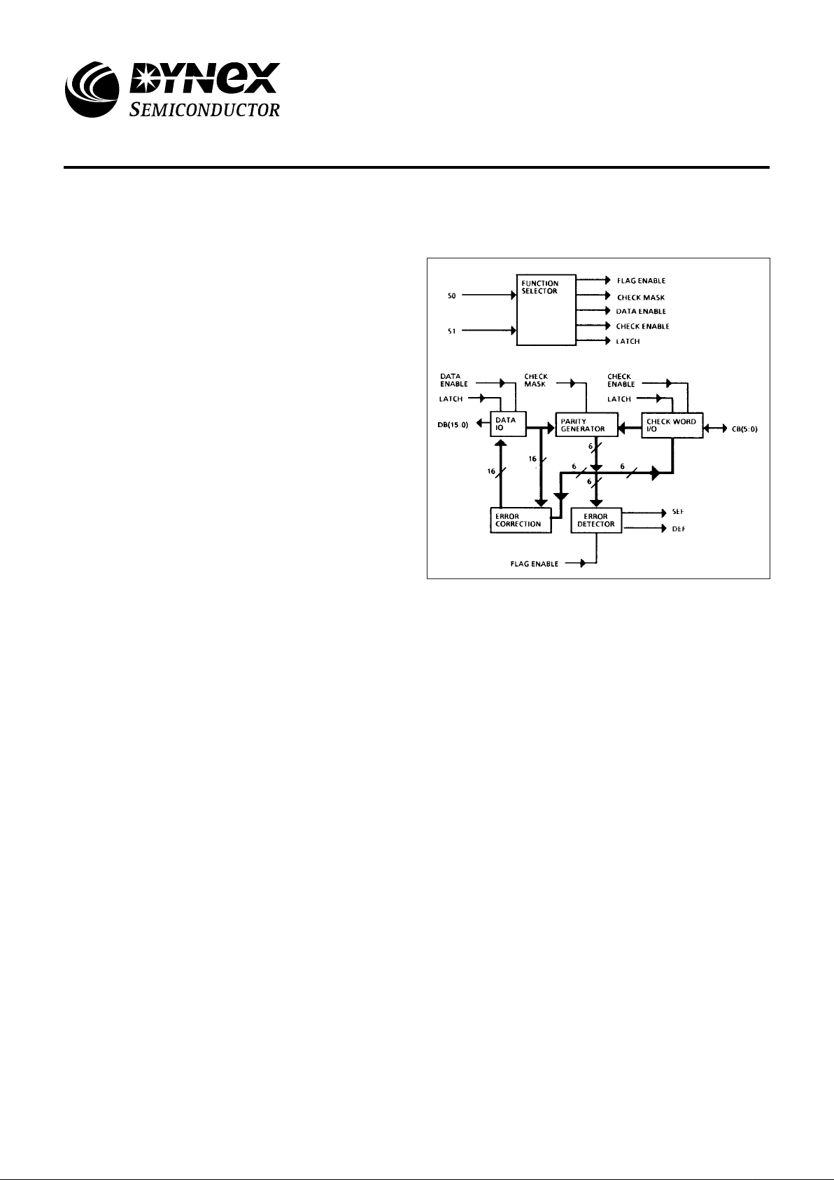
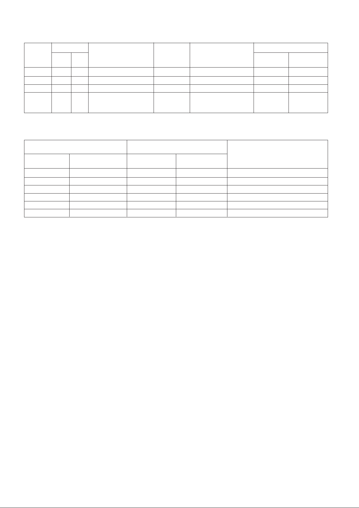
The control signals S1 and S0 select the function to be
performed by the EDAC They control the generation of check
words and the latching and correction of data (see table 1)
When errors are detected, flags are placed on outputs SEF
and DEF (see table 2).
Figure 1: Block Diagram
FEATURES
■ Radiation Hard:
Dose Rate Upset Exceeding 3x10
10
Rad(Si)/sec
Total Dose for Functionality Upto 1x10⁶ Rad(Si)
■ High SEU Immunity, Latch Up Free
■ CMOS-SOS Technology
■ All Inputs and Outputs Fully TTL Compatible (54HST630)
or CMOS Compatible (54HSC630)
■ Low Power
■ Detects and Corrects Single-Bit Errors
■ Detects and Flags Dual-Bit Errors
■ High Speed:
Write Cycle - Generates Checkword In 40ns Typical
Read Cycle - Flags Errors In 20ns Typical
54HSC/T630
Radiation hard 16-Bit ParallelError
Detection & Correction
Replaces June 1999 version, DS3595-4.0 DS3595-5.0 January 2000

54HSC/T630
2/10
Table 1: Control Functions
Control Error Flags
Cycle S1 S0 EDAC Function Data UO Checkword SEF DEF
WRITE Low Low Generates Checkword Input Data Output Checkword Low Low
READ Low High Read Data BCheckword Input Data Input Checkword Low Low
READ High High Latch & Flag Error Latch Data Latch Checkword Enabled Enabled
READ High Low Correct Data Word & Output Output Syndrome Bits Enabled Enabled
Generate Syndrome Bits Corrected
Data
Table 2: Error Functions
Total Number of Errors Error Flags Data Correction
16-bit Data 6-bit Checkword SEF DEF
0 0 Low Low Not Applicable
1 0 High Low Correctlon
0 1 High Low Correction
1 1 High High Interrupt
2 0 High High Interrupt
0 2 High High Interrupt
ERROR DETECTION & CORRECTION
During a memory write cycle, six check bits (CBO-CB5)
are generated by eight-input parity generators using the data
bits defined in Table 3. During a memory read cycle, the 6-bit
checkword is retrieved along with the actual data.
Error detection is accomplished as the 6-bit checkword and
the 16-bit data word from memory are applied to internal parity
generators/checkers. If the parity of all six groupings of data
and check bits are correct, it is assumed that no error has
occurred and both error flags will be low. It should be noted
that the sense of two of the check bits, bits CBO and CB1, is
inverted to ensure that the gross-error condition of all lows and
all highs is detected.
If the parity of one or more of the check groups is incorrect,
an error has occurred and the proper error flag or flags will be
set high. Any single error in the 16bit data word will change the
sense of exactly three bits of the 6-bit checkword. Any single
error in the 6bit checkword changes the sense of only that one
bit. In either case, the single error flag will be set high while the
dual error flag will remain low.
Any two-bit error will change the sense of an even number
of check bits. The two-bit error is not correctable since the
parity tree can only identify singlebit errors. Both error flags are
set high when any two-bit error is detected.
Three or more simultaneous bit errors cause the EDAC to
transmit that no error, a correctable error, or an uncorrectable
error has occurred and hence produce erroneous results in all
three cases.
Error correction is accomplished by identifying the bad bit
and inverting it. Identification of the erroneous bit is achieved
by comparing the 16-bit word and 6-bit checkword from
memory with the new checkword with one (checkword error)
or three (data word error) inverted bits.
As the corrected word is made available on the data word l/
O port, the checkword l/O port presents a 6-bit syndrome error
code. This syndrome code can be used to identify the
corrupted bit in memory (see Table 4. overleaf).

54HSC/T630
3/10
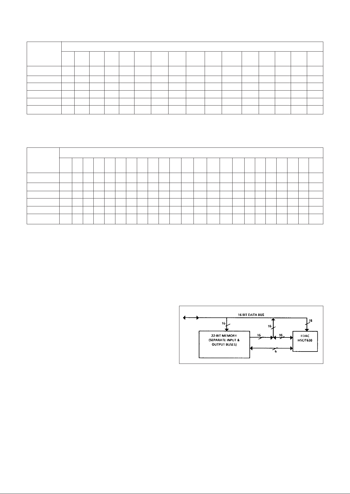
14
X
X
X
13
X
X
X
12
X
X
X
11
X
X
X
10
X
X
X
9
X
X
X
8
X
X
X
16-bit Data Word
Checkword
Bit
CB0
CB1
CB2
CB3
CB4
CB5
2
X
X
X
15
X
X
X
7
X
X
X
6
X
X
X
5
X
X
X
4
X
X
X
1
X
X
X
3
X
X
X
0
X
X
X
The six check bits are partly bits derived from the matrix of data bits as indicated by 'X' for each bit.
Table 3: Check Word Generation
Error Location
DB15
H
H
L
H
L
L
CB0
L
H
H
H
H
H
CB1
H
L
H
H
H
H
CB2
H
H
L
H
H
H
CB3
H
H
H
L
H
H
CB4
H
H
H
H
L
H
CB5
H
H
H
H
H
L
No
Error
H
H
H
H
H
H
DB0
L
L
H
L
H
H
DB1
L
H
L
L
H
H
DB2
H
L
L
L
H
H
DB3
L
L
H
H
L
H
DB4
L
H
L
H
L
H
DB5
H
L
L
H
L
H
DB6
H
L
H
L
L
H
DB7
H
H
L
L
L
H
DB8
L
L
H
H
H
L
DB9
L
H
L
H
H
L
DB10
L
H
H
L
H
L
DB11
H
L
H
L
H
L
DB12
H
H
L
L
H
L
DB13
L
H
H
H
L
L
DB14
H
L
H
H
L
L
Syndrome
Error
Code
CB0
CB1
CB2
CB3
CB4
CB5
Table 4: Error Syndrome Codes
APPLICATIONS
Although many semiconductor memories have separate
input and output pins, it is possible to design the error
detection and correction function using a single EDAC. EDAC
data and check bit pins function as inputs or outputs
dependent upon the state of control signals S0 and S1. It
becomes necessary to use wired AND logic, with fairly
complex timing system, to control the EDAC and data bus.
This scheme becomes difficult to implement both in terms of
board layout and timing. System performance is also
adversely affected, See Figure 2.
Optimised systems can be implemented using two EDAC’s
in parallel, One of the units is used strictly as an encoder
during the memory write cycle. Both controls S0 and Sl are
grounded, The encoder chip will generate the 6-bit check word
for memory storage along with the 16-bit data.
The second of the two EDAC’s will be used as a decoder
during the memory read cycle. This decoder chip requires
timing pulses for correct operation. Control S1 is set low and
S0 high as the memory read cycle begins. After the memory
output data is valid, the control S1 input is moved from the low
to a high. This low-to-high transition latches the 22-bit word
from memory into internal registers of this second EDAC and
enables the two error flags. If no error occurs, the CPU can
accept the 16-bit word directly from memory. If a single error
has occurred, the CPU must move the control SO input from
the high to a low to output corrected data and the error
syndrome bits. Any dual error should be an interrupt condition.
In most applications, status registers will be used to keep
tabs on error flags and error syndrome bits. If repeated
patterns of error flags and syndrome bits occur, the CPU will
be able to recognize these symptoms as a “hard” error. The
syndrome bits can be used to pinpoint the faulty memory chip,
See Figure 3.
Figure 2: Error Detection and Correction Using a
Single EDAC Unit
 Loading...