

Page 1
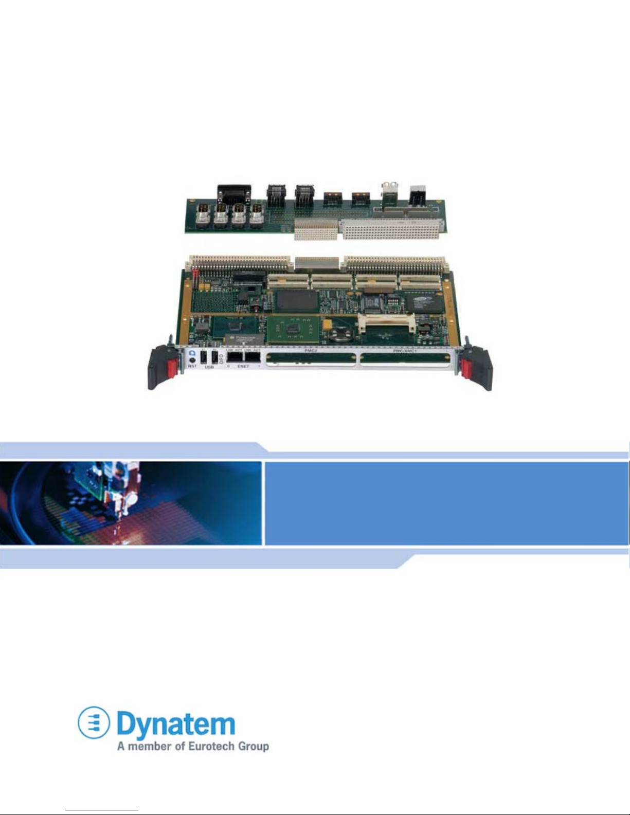
USER MANUAL
DPDMAN103A Updated 14 Dec 2012
CPU-71-10 (DPD/RPD/XPD)
VMEbus Intel® Core™ Duo
Single Board Computer
Page 2

CPU-71-10 (XPD) User’s Manual Rev. 1.03
Revised to fix JP8 description
December 2012
Dynatem
23263 Madero, Suite C
Mission Viejo, CA 92691
Phone: (949) 855-3235
Fax: (949) 770-3481
www.dynatem.com
Page 3

Table of Contents
1. Features 1
2. Related Documents 3
3. Hardware Description 5
3.1 Overview 5
3.2 Processor 6
3.3 Chipset 6
3.4 DRAM 7
3.5 Intel 82571EB Dual Gigabit Ethernet Controller 7
3.6 Silicon Motion SM712 Graphics Processor 8
3.7 Tundra Universe IID CA91C142D PCI-VMEbus Interface 9
3.8 PCI Mezzanine Card (PMCX) and XMC Expansion 12
3.9 Intel’s FW82802A Firmware Hub Holds the System BIOS In Flash Memory 12
3.10 Clock Drivers 12
3.11 Reset Circuitry 13
3.12 Watchdog Timer Operation 14
4. Installation 15
4.1 Jumper Selectable Options 15
4.2 CompactFlash Drive Installation 17
4.3 PCI Mezzanine Card (PMC) Installation 17
4.4 VMEbus Chassis Installation 17
4.5 Front Panel Connectors and Reset Switch 18
Dynatem CPU-71-10 (XPD) VMEbus Core 2 Duo Processor Board – User’s Manual i
Page 4

A. Connector Pin-outs 19
A.1 Front Panel USB Connector (USB1 & USB2) 20
A.2 1000BaseTX Fast Ethernet Front Panel Connector (J1) 20
A.3 CompactFlash Interface Connector (J3) 21
A.4 VMEbus Connectors (P1, P2, and P0) 22
A.5 PCI-X Mezzanine Card Connectors (JN1, JN2, JN3, and JN4) and XMC Connector (J15) 25
B. BIOS & Setup 31
B.1 Redirecting to a Serial Port 31
B.2 Setup Menus 31
B.3 Navigating Setup Menus & Fields 32
B.4 Main Setup Menu 33
B.5 Exit Setup Menu 34
B.6 Boot Setup Menu 35
B.7 POST Setup Menu 37
B.8 PnP Setup Menu 39
B.9 Super I/O (SIO) Setup Menu 40
B.10 Features Setup Menu 41
B.11 Firmbase Setup Menu 42
B.12 Miscellaneous Setup Menu 44
C. Power and Environmental Requirements 47
D. XPDPTB Rear Plug-in I/O Expansion Module for the XPD 49
D.1 XPDPTB Connector Pin-outs 50
ii CPU-71-10 (XPD/RPD/DPD) VMEbus Core 2 Duo Processor Board – User’s Manual
Page 5
Chapter 1 – Features
1. Features
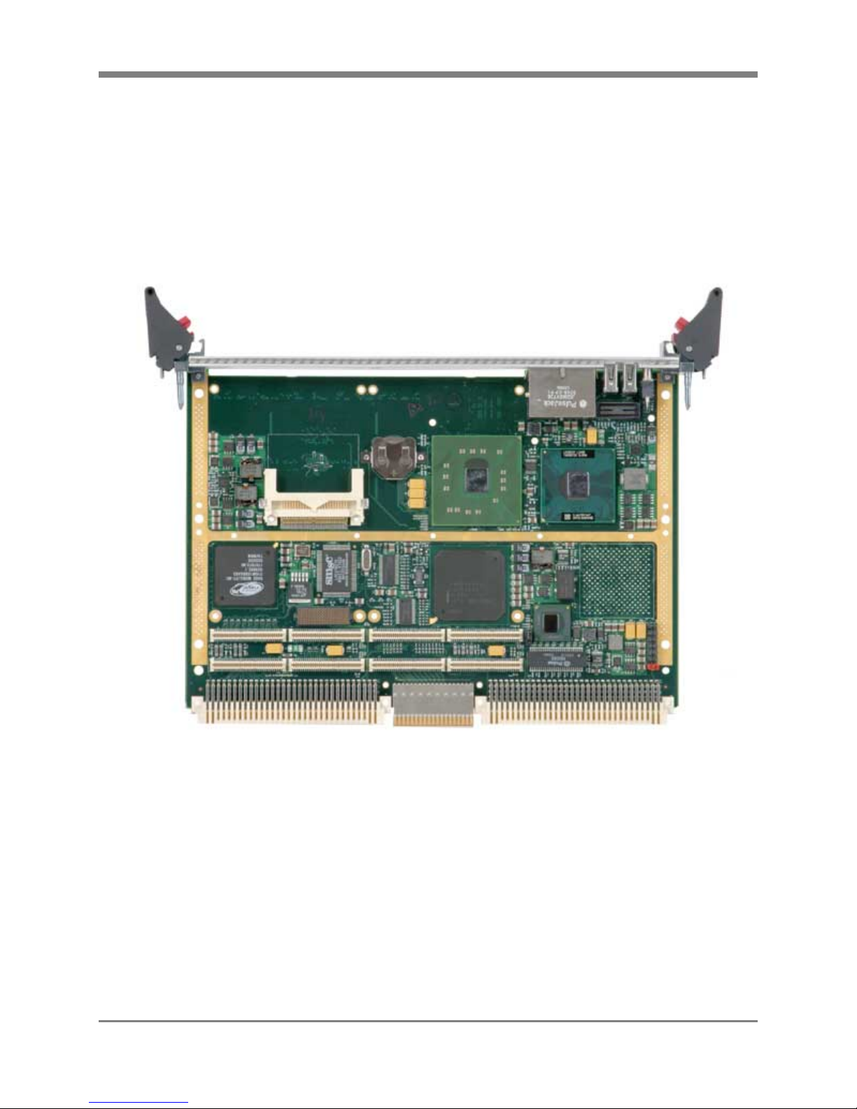
The CPU-71-10 (also known as the XPD / DPD / RPD) is a single-slot 6U VMEbus Single Board Computer (SBC).
The XPD offers full PC performance with a Core Duo processor. The XPD is available in two versions: the lower
cost DPD for standard industrial applications and the 1101.2 compliant, conduction-cooled RPD with wedgelocks,
stiffener bar, and a full board heatsink for rugged applications. When referring to attributes of both versions, we
will use the common name XPD. The XPD employs Intel’s embedded technology to assure long-term availability.
Features of the XPD include:
A 1.5 GHz Intel® Core2™ Duo L7400 processor with 4 MB of L2 cache
Single-slot VMEbus operation with on-board CompactFlash disk for bootable mass storage and front panel
connectors for two USB 2.0 ports, two Fast Ethernet ports, and XPD & PMC I/O
An IDE port, four RS232 COM ports, PS/2 Mouse & Keyboard, two USB ports, and PMC I/O are routed out to
the backplane via the P2 connector
Two Serial ATA ports, VGA graphics, two Gbit Ethernet ports (Vita 31.1 compliant) and PMC/XMC I/O are
routed to the P0 connector
CPU-71-10 (XPD/RPD/DPD) VMEbus Core 2 Duo Processor Board – User’s Manual 1
Page 6

Chapter 1 – Features
The Intel® E7520 Memory Controller Hub (MCH) and Intel® 6300ESB I/O Controller Hub (ICH) provide
high-speed memory control, 16 lanes of PCI Express I/O, integrated I/O like Serial ATA, USB 2.0, IDE
supporting Ultra 100 DMA Mode for transfers up to 88.88 MB/sec, and 64 bit PCI-X bus transfers at 66 MHz
Silicon Motion’s SM712 VGA Controller
Two Intel 82571EB Ethernet Controllers with a x4 PCI Express interface, each offering two
10/100/1000BaseTX support; two ports are routed to P0 in compliance with Vita 31.1 for backplane fabric
switching while the other two are routed to the front panel
4 GB of DDR2-400 DRAM provided on-board
Tundra Universe IID PCI-VMEbus Interface provides 64-bit VMEbus transfer rates over 30 MB/sec. Integral
FIFOs permit write-posting to maximize available PCI and VMEbus bandwidth. Full Slot 1 (System
Controller) functionality is provided
PCI Mezzanine Card (PMC) expansion supports 64 bits @ up to 66 MHz
A second PCI Mezzanine Card (PMC) expansion supports 64 bits @ up to 66 MHz and can also support an MC
module with up to x8 PCI Express
Secondary IDE port for CompactFlash on-board for flash-based or mechanical mass storage for 1 slot booting
General Software’s Version 6.0 flash-based system BIOS
PXE for diskless booting over Ethernet
Programmable watchdog timer for system recovery and a CPLD for LED control, Geographical Addressing,
and Built-In Test (BIT) status and control
Operating System (OS) and driver support, including Windows NT, Embedded NT, XP, QNX, VxWorks,
Linux, Solaris, and pSOS+.
2 CPU-71-10 (XPD/RPD/DPD) VMEbus Core 2 Duo Processor Board – User’s Manual
Page 7

Chapter 2 – Related Documents
2. Related Documents
Listed below are documents that describe the Pentium processor and chipset, and the peripheral components used on
the XPD. Either download from the Internet or contact your local distributor for copies of these documents.
The XPD uses the L2400 Low Voltage Core Duo. For information on this processor, go to:
http://ark.intel.com/products/28026?wapkw=l7400
For the ICH component in the 6300ESBchipset get the Intel ® 6300ESB I/O Controller Hub Datasheet. It is document
number 300641-002.
ftp://download.intel.com/design/intarch/datashts/30064102.pdf
For information on the E7520 MCH component in the chipset, please go to:
http://www.intel.com/design/chipsets/embedded/e7520_7320.htm
For data sheets on I/O controllers:
82571EB Fast Ethernet PCI Controller
http://www.intel.com/design/network/products/lan/controllers/82571eb.htm
VMEbus Interface Components Manual
Tundra Semiconductor Corporation; Universe IID revisions are found at www.tundra.com
The following documents provide information on the PC architecture and I/O:
PCI Local Bus Specification, Revision 2.2
http://www.pcisig.com/specifications/
PCI-X Specification, Revision 1.0A
http://www.pcisig.com/specifications/
System Management Bus Specification (SMBus), Revision 1.1
http://www.smbus.org/specs/
Universal Serial Bus Specification
http://www.usb.org/developers
The following documents cover topics relevant to the VMEbus and can be purchased through VITA:
IEEE Std 1014-1987, IEEE Standard for a Versatile Backplane Bus: VMEbus
The Institute of Electrical and Electronic Engineers
345 East 47th Street
New York, NY 10017
(800) 678-4333
Wade D. Peterson, The VMEbus Handbook
VITA
10229 North Scottsdale Road, Suite B
Scottsdale, AZ 85253
(480) 951-8866
CPU-71-10 (XPD/RPD/DPD) VMEbus Core 2 Duo Processor Board – User’s Manual 3
Page 8

Chapter 2 – Related Documents
The following documents are the current draft standards for the PCI Mezzanine Card (PMC) and XMC cards:
IEEE Draft Std P1386/2.0, Draft Standard for a Common Mezzanine Card Family: CMC
The Institute of Electrical and Electronic Engineers
345 East 47th Street
New York, NY 10017
(800) 678-4333
IEEE Draft Std P1386.1/2.0, Draft Standard Physical and Environmental Layers for PCI Mezzanine Cards:
PMC
The Institute of Electrical and Electronic Engineers
345 East 47th Street
New York, NY 10017
(800) 678-4333
VITA 42.0, XMC Switched Mezzanine Card Auxiliary Standard
VITA
10229 North Scottsdale Road, Suite B
Scottsdale, AZ 85253
(480) 951-8866
4 CPU-71-10 (XPD/RPD/DPD) VMEbus Core 2 Duo Processor Board – User’s Manual
Page 9
Chapter 3 – Hardware Description
3. Hardware Description
3.1 Overview
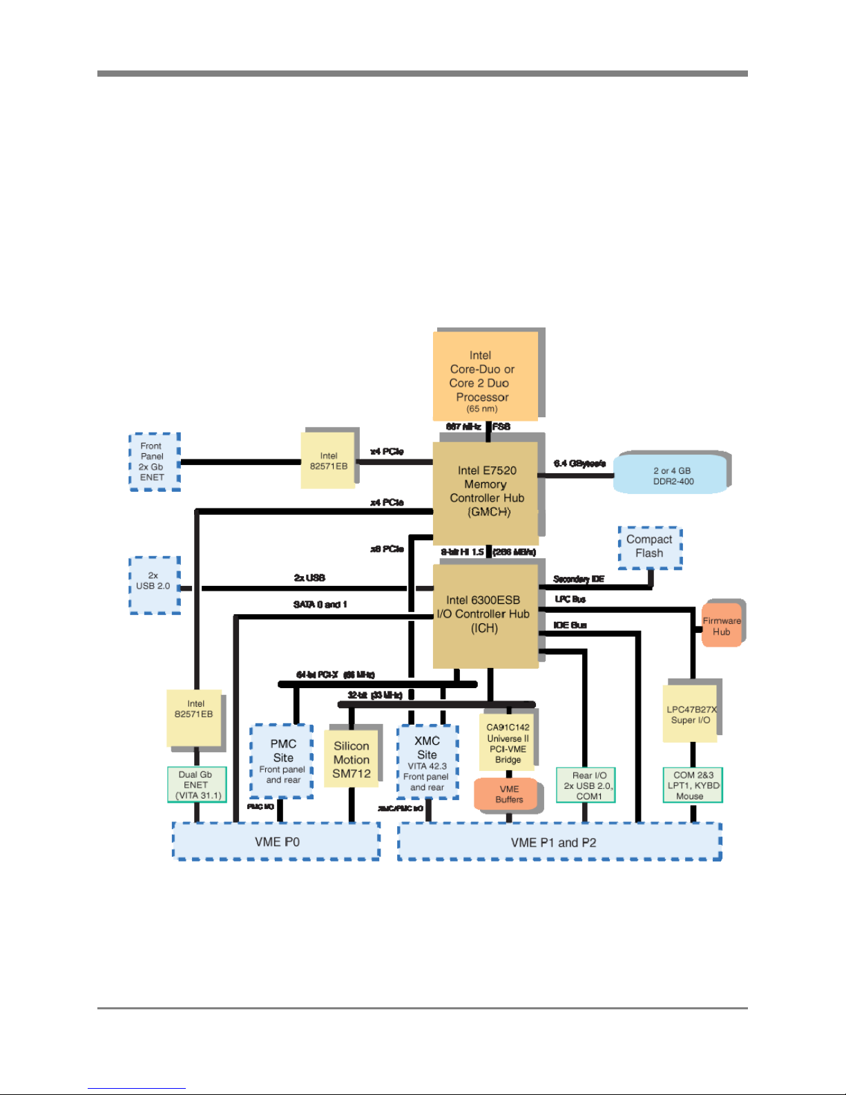
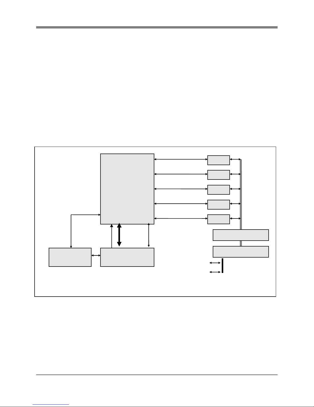
The block diagram of the XPD is shown below. The sections that follow describe the major functional blocks of the
XPD.
CPU-71-10 (XPD/RPD/DPD) VMEbus Core 2 Duo Processor Board – User’s Manual 5
Page 10

Chapter 3 – Hardware Description
3.2 Processor
The XPD supports a Core Duo processor at 1.66 GHz. The Intel Core Duo processor with 2 MB of L2 cache is the
first dual core processor available for mobile and embedded applications. Features include:
667 MHz front side bus (limited by the E7520 FSB).
On-die 4 MB of L2 cache with Advanced Transfer Cache Architecture.
On-die, primary 32-KB instruction cache and 32-KB write-back data cache.
Second-generation Streaming SIMD Extensions 2 (SSE2) and streaming SIMD Extensions 3 (SSE3)
Supports Intel® Architecture and Dynamic Execution.
For further information on the Core2 Duo processor available from Intel Corporation, search at:
http://ark.intel.com/products/28026?wapkw=l7400
The Intel® Core™ Duo processor was designed to deliver high, dual processor high performance with low power
consumption. With its 65 nm processing technology and 2 MB of L2 advanced transfer cache, the Core Duo offers
more performance per Watt. The Thermal Design Power (TDP) is 15 W. Advanced power management included
Enhanced Intel SpeedStep Technology are supported. SpeedStep enables clock and core voltage throttling based on
temperature or processor loading.
The processor’s 667 MHz Front Side Bus utilizes a split-transaction, deferred reply protocol. The FSB uses a
Source-Synchronous Transfer (SST) of address and data to improve performance by transferring data four times per
bus clock. The address bus can deliver addresses twice per clock cycle. Together, the 4X data bus and 2X address
bus provide a data bus bandwidth of up to 5.33 GB/second.
3.3 Chipset
The Intel® E7520 Memory Controller Hub (MCH) and Intel® 6300ESB I/O Controller Hub (ICH) chipset provide
memory control, mass storage and basic I/O, and standard PC system resources including the real time clock, NVRAM, timers, thermal management, and interrupt management. Also, the MCH provides 24 lanes of PCI Express
expansion (16 of which are implemented on the XPD) for high-speed expansion through the two dual 1000BaseTX
controller chips and the XMC site.. The ICH supports a 32 bit @ 33 MHz PCI bus, to support the Universe
VMEbus interface controller and the Silicon Motion SM712 graphics chip, and a 64 bit @ 66 MHz PCI-X bus for
user I/O expansion through the two PMC sites. The ICH also provides a Low Pin Count (LPC) interface for the
BIOS flash chip and for Super I/O and an SMBus interface for on-board resources like the DRAM circuit’s SPD
PROMs and the thermal monitors.
The MCH supports a base system bus frequency of 200 MHz. The address and request interface is double pumped
to 400 MHz while the 64-bit data interface (+ parity) is quad pumped to 800 MHz. This provides a matched system
bus address and data bandwidth of 6.4 GB/s. The E7520 (MCH) provides a 400 MHz interface to DDR2 RAM (72
bits wide with ECC). The XPD can be populated with one or two banks of DRAM for 2 GB or 4 GB of total
memory respectively. Each bank is serviced by a separate channel from the MCH that function in lock-step mode.
Memory controller features include:
Memory mirroring allows for two copies of all data in the memory subsystem (one on each channel) to be
maintained.
Hardware periodic memory scrubbing, including demand scrub support.
6 CPU-71-10 (XPD/RPD/DPD) VMEbus Core 2 Duo Processor Board – User’s Manual
Page 11

Chapter 3 – Hardware Description
Retry on uncorrectable memory
ECC is supported
DDR2-400 DRAM is supported on-board
The 6300ESB I/O Controller Hub (ICH) provides most of the XPD’s on-board I/O and it’s the XPD’s PCI-X
expansion bridge. The ICH is designed as a low-power, high-performance I/O hub that features:
64-bit @ 66 MHz PCI-X expansion that is used on the XPD for the two on-board PMC-X slots.
Four USB 2.0 compliant ports: two of which are routed to the front panel while the other twoare routed to
the P2 connector to the backplane.
Integrated IDE controller supports Ultra 100 DMA Mode Transfers up to 100 MB/sec read cycles and
88.88 MB/sec write cycles for a CompactFlash drive on-board and a primary IDE port that is routed
through P2 to the XPDPTB
Two Serial ATA ports providing 150 MB/sec data rates are routed through P0
Standard PC functionality like a battery-backed RTC and 256-bytes of CMOS RAM, Power Management
Logic, Interrupt Controller, Watchdog Timer, AC’97 CODEC, Integrated 16550 compatible UART’s, and
multimedia timers based on the 82C54
For further information, see the documents referenced in Section 2
3.4 DRAM
The XPD supports two 72-bit wide, DDR2-400 memory interface channels with a memory bandwidth of 6.4 GB/s
with ECC. The XPD can be populated to support 2GB or 4GB of DRAM.
3.5 Intel 82571EB Dual Gigabit Ethernet Controller
The XPD supports two Intel® 82571EB Gigabit Ethernet Controllers, one provides two Vita 31.1 compliant Gigabit
LAN ports to the backplane while the other provides two that are accessible from the front panel. The 82571EB is a
single, compact component with two fully integrated Gigabit Ethernet Media Access Control (MAC) and physical
layer (PHY) ports. This device uses the PCI Express* architecture (Rev. 1.0a), and also enables a dual-port Gigabit
Ethernet implementation in a very small area, which is useful for embedded designs with critical space constraints.
The Intel 82571EB Gigabit Ethernet Controller provides two IEEE 802.3 Ethernet interfaces for 1000BASE-T,
100BASE-TX, and 10BASE-T applications. In addition to managing MAC and PHY Ethernet layer functions, the
controller manages PCI Express packet traffic across its transaction, link, and physical/logical layers.
The Intel 82571EB Gigabit Ethernet Controller for PCI Express is designed for high performance and low memory
latency. The device is optimized to connect to the E7520 MCH using four PCI Express lanes. Alternatively, the
controller can connect to an Input/Output (I/O) Control Hub (ICH) that has a PCI Express interface. Wide internal
data paths eliminate performance bottlenecks by efficiently handling large address and data words. Combining a
parallel and pipelined logic architecture optimized for Gigabit Ethernet and for independent transmit and receive
queues, the controller efficiently handles packets with minimum latency. The controller includes advanced interrupthandling features and uses efficient ring-buffer descriptor data structures, with up to 64 packet descriptors cached
on chip. A large 48 KByte per port on-chip packet buffer maintains superior performance. In addition, using
hardware acceleration, the controller offloads tasks from the host, such as checksum calculations for transmission
control protocol (TCP), user datagram protocol (UDP), and Internet protocol (IP); header and data splitting; and
TCP segmentation.
CPU-71-10 (XPD/RPD/DPD) VMEbus Core 2 Duo Processor Board – User’s Manual 7
Page 12
Chapter 3 – Hardware Description
The Intel 82571EB offers the following features:
10, 100, and 1000BaseTX support with auto-negotiation
Uses x4 PCI Express from MCH
Dual 48 KB configurable RX and TX packet FIFOs
Built-in Phyceiver
Serial EEPROM for non-volatile Ethernet address storage
Both 10/100/1000BaseTX ports of one 82571EB device are brought out to the P0 backplane connector in
compliance with the VITA 31.1 specification. VITA 31.1permits fabric switching on the backplane where 31.1
compliant SBC’s can communicate with each other and with an external network through switch modules that are
located at either end of the backplane. Optionally these two 1 Gb Ethernet ports are brought to industry standard
RJ-45 connectors on Dynatem’s rear I/O plug-in module (XPDPTB).
nd
The two Ethernet ports provided by the DPD’s 2
Technical documents on Intel’s 82571EB Dual Gigabit Ethernet Controller are available at:
http://www.intel.com/design/network/products/lan/docs/82571eb_docs.htm
82571EB are accessible from the front panel.
3.6 Silicon Motion SM712 Graphics Processor
The Silicon Motion SM712 processor generates VGA graphics which are routed to the P0 backplane connector. A
VGA connector is provided by the optional XPDPTB rear-I/O module.
The SM712’s features include:
Up to 1280x1024 or higher resolution with programmable PLL (SM712 up to 1024x768)
128-bit 2D graphic engine
4MB embedded SDRAM
The SM712 offers low power graphics for limited GUI purposes. It attaches to the system via the ICH’s 32 bit @
33 MHz PCI bus.
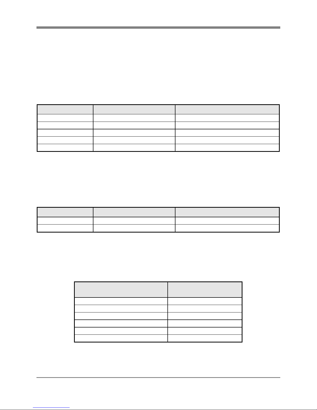
Silicon Motion SM712 Signal PCI Bus Connection
Bus PCI
IDSEL AD17
REQ# REQ1#
GNT# GNT1#
INTR# INTB#
8 CPU-71-10 (XPD/RPD/DPD) VMEbus Core 2 Duo Processor Board – User’s Manual
Page 13
Chapter 3 – Hardware Description
3.7 Tundra Universe IID CA91C142D PCI-VMEbus Interface
The PCI-VMEbus interface, based on the Tundra Universe IID CA91C142D, offers the following features:
High-performance 64-bit VMEbus interface.
Integral FIFOs for write-posting allow the Universe IID to quickly relinquish the bus.
Programmable DMA controller with linked list support.
Full VMEbus system controller functionality.
Complete VMEbus address and data transfer modes: A32/A24/A16 master and slave; D64
(MBLT)/D32/D16/D08 master and slave.
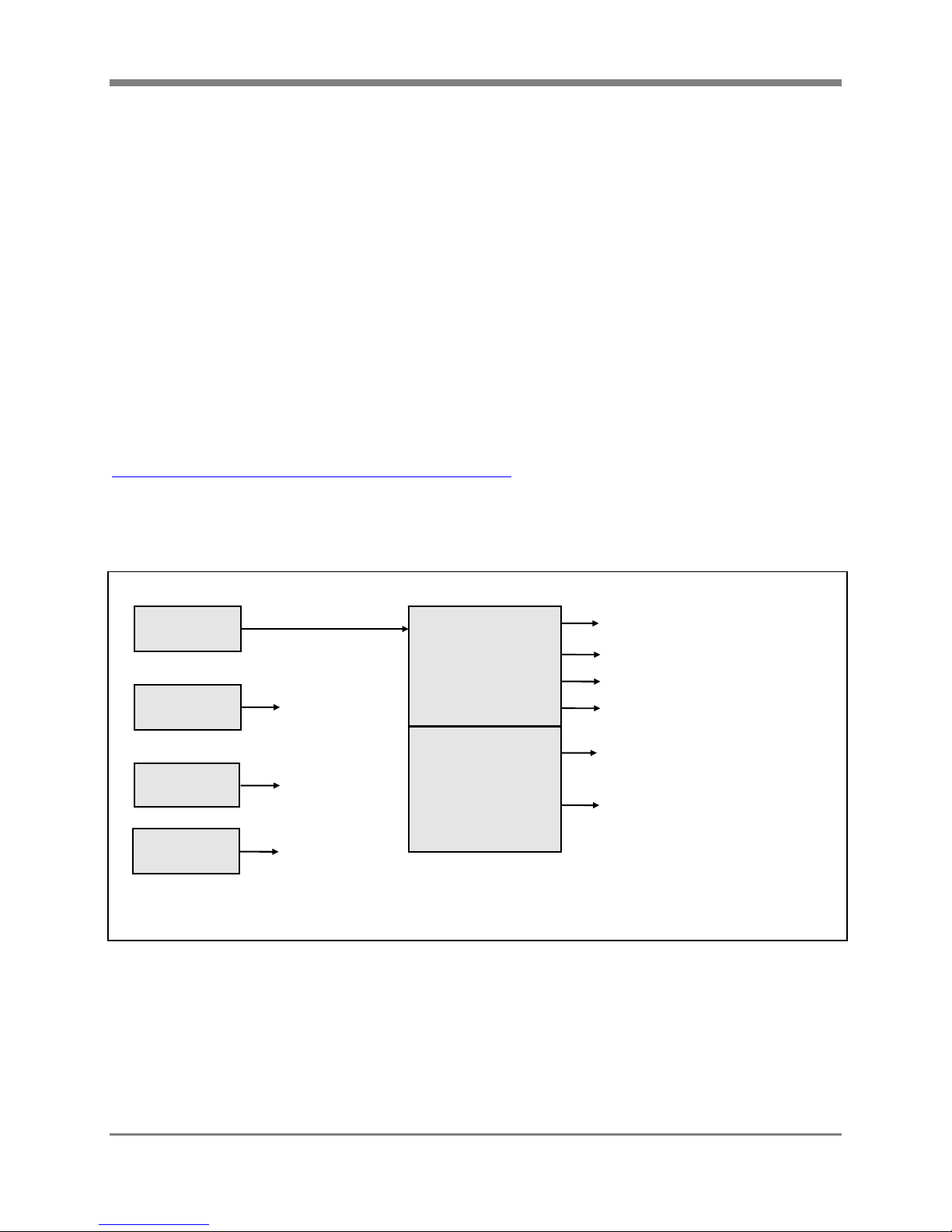
The block diagram of the PCI-VMEbus interface is shown below:
Universe IID
CA91C142D
IDSEL is
AD19
Reset Circuitry I/O Controller Hub ICH
PCI Bus
AD[31:0]
A01 – A31, LWORD*
D00 – D31
AS, DS0*, DS1*, Ctrl
AM0* – AM5*
IRQx*, BRx*
INTG#, REQ1#, GNT1#
Low Pin Count (LPC) Bus
Buffers
Buffers
Buffers
Buffers
Buffers
VMEbus P1 Connector
VMEbus P2 Connector
P2 User Defined Pins
VMEbus
PCI-VMEbus Interface Block Diagram
CPU-71-10 (XPD/RPD/DPD) VMEbus Core 2 Duo Processor Board – User’s Manual 9
Page 14

Chapter 3 – Hardware Description
As shown in the block diagram, several peripheral signals are routed to the user-defined pins of the VMEbus P2
connector: the IDE bus and the LPC bus which routes to a Super I/O chip on the XPDPTB rear plug-in card for I/O
expansion. The VMEbus P1 and P2 connector pin-outs are given in Appendix A.
The Universe IID CA91C142D can act as a PCI bus initiator (master) or target (slave), and a VMEbus master or
slave. The Universe IID is capable of generating interrupts on the VMEbus, and can act as a VMEbus interrupt
handler. The Universe IID provides full VMEbus system controller functionality. The XPD reset circuitry is tied to
the Universe IID, since the XPD can generate the VMEbus SYSRESET* signal as well as be reset by another
VMEbus board that asserts the SYSRESET* signal. The XPD reset circuitry is discussed in detail in Section 3.12.
This section is intended to supplement the VME-to-PCI Bus Bridge Manual User Manual (downloadable from
www.tundra.com), which contains comprehensive descriptions of the operation and programming of the Universe
IID. That manual provides the necessary information to understand the operating modes of the Universe IID:
XPD-initiated transfers (PCI slave, VMEbus master).
Other VMEbus master-initiated transfers (PCI master, VMEbus slave).
DMA controller transfers (PCI master, VMEbus master).
VMEbus interrupt generation.
VMEbus interrupt handling.
System controller functionality.
Register programming via the PCI bus and the VMEbus.
Coupled and uncoupled transfers between the PCI bus and the VMEbus.
4 mailboxes and 8 semaphores.
VMEbus arbitration.
The Universe IID Control and Status Registers (UCSRs) are used for the configuration of the Universe IID. These
registers form a 4 KB block, divided into three groups:
PCI Configuration Space (PCICS).
Universe IID Device Specific Status Registers (UDSRs).
VMEbus Control and Status Registers (VCSRs).
These registers are accessible (to varying degrees) via three address spaces:
PCI Configuration Space – Only the PCICS register block is accessible in this space.
PCI Memory Space – The entire 4 KB UCSR block is accessible in this space.
VMEbus A32/A24/A16 Space – The entire 4 KB UCSR block is accessible in this space.
10 CPU-71-10 (XPD/RPD/DPD) VMEbus Core 2 Duo Processor Board – User’s Manual
Page 15
Chapter 3 – Hardware Description
During initialization, the system BIOS maps PCI peripherals that require space beyond the PCI configuration space
into the memory space or I/O space. The Universe IID UCSR block is 4 KB in size and must be aligned on a 64 KB
boundary. The total I/O space of an Intel processor is 64 KB and many of the common PC peripherals are found in
the first 1 KB of this space. Thus, a request for a 64 KB block of I/O space for the Universe IID registers would be
denied by the system BIOS, leaving the Universe IID unmapped. To avoid this situation, the Universe IID offers a
power-up option to map its registers into the memory space. This is accomplished on the XPD by tying the VA[1]
line high via a pull-up resistor.
There are two mechanisms to access the UCSR block from the VMEbus. The first is the VMEbus Register Access
Image (VRAI) method, which is defined by the following registers in the Universe IID User’s Manual:
Field Register Bits Description
Address Space VAS in Table A.76 A32, A24, or A16
Base Address BS[31:12] in Table A.77 Lowest address in the 4 KB slave image
Slave Image Enable EN in Table A.76 Enable VMEbus Register Access Image
Mode SUPER in Table A.76 Supervisor and/or Non-Privileged
Type PGM in Table A.76 Program and/or Data
The reset state of the VAS, BS[31:12], and EN fields can be configured as power-up options. On the XPD, all of
these fields reset to 0. Thus, the VRAI method must be configured and enabled by accessing the Universe IID
registers in the memory space.
The second mechanism for accessing the UCSR block from the VMEbus is the CS/CSR method, which is defined
by the following registers in the Universe IID section of the User’s Manual:
Field Register Bits Description
Base Address BS[23:19] in Table A.84 Base address of Universe IID 512 KB slot
Slave Image Enable EN in Table A.78 Enable CS/CSR image
The BS[23:19] and EN fields reset to all 0s, and the EN bit can be set by the VME64 Auto ID process. Thus, the
CR/CSR method must be configured by accessing the Universe IID registers in the memory space.
The PCI signals specific to the Tundra Universe IID CA91C142D are routed from the PCI bus of the ICH and they
are shown below:
Tundra Universe IID CA91C142D
PCI Bus Connection
Signal
Bus PCI
IDSEL AD16
REQ# REQ0#
GNT# GNT0#
LINT0# INTA#
LINT1# Pulled Up
CPU-71-10 (XPD/RPD/DPD) VMEbus Core 2 Duo Processor Board – User’s Manual 11
Page 16
Chapter 3 – Hardware Description
3.8 PCI-X Mezzanine Card (PMCX) and XMC Expansion
The XPD supports two PCI-X Mezzanine Card (PMC-X) sites on-board. Site #1 also supports x8 XMC cards. Site
#1 routes I/O from J14 out through the P2 connector (please see Appendix A) or it can be accessed from the front
panel. Site #2 routes I/O from J24 to the P0 backplane connector and/or to the front panel.
3.9 Intel’s FW82802AC Firmware Hub Holds the System BIOS In Flash Memory
The Intel FW82802AC uses a 5-pin interface and provides 1 MByte of flash memory for the system BIOS. This
device can fill the 1 MB real mode memory map so only a portion its upper 256 MB is used. The FW82802AC’s 1
MB of memory space is segmented into sixteen parameter blocks of 64 KB each. The XPD powers up into real
mode and the BIOS is eventually shadowed into system DRAM after booting through the BIOS.
The ICH provides the 5-pin interface to the E82802AC. The upper 256 KB of the E82802AC is located from
000C0000 - 000FFFFF and its full 1 MB of memory is aliased from FFF00000 – FFFFFFFF where it can be fully
accessed after booting up through the BIOS.
Here’s a link to a datasheet for the 82802AC:
ftp://download.intel.com/design/chipsets/datashts/29065804.pdf
3.10 Clock Drivers
The clock driver circuitry is shown below:
14.31818 MHz
Crystal
32.768 KHz
Crystal
Two 25.0 MHz
Oscillators
64.0 MHz
Oscillator
To ICH for
Real Time
Clock
To Ethernet
Controllers
82571EB &
82571EB and
To Universe
IID CLK64
932S208
100 MHz differential
clocks for MCH, ICH,
ITP, & CPU clocks
48 MHz
Routed to ICH for
USB and UART’s and
to the MCH for
Graphics
Core Duo CPU
To MCH for SDRAM Clocks
ICH
ITP Port
To ICH for USB & Serial
To MCH for dot clocks
Clock Driver Circuitry
The clocks are generated by the 932S208, which is driven by a 14.31818 MHz crystal. DRAM clocks are
synthesized by the MCH and Hub Interface and PCI(-X) clocks are produced by the ICH. A 32.768 KHz Crystal
drives the Real Time Clock (RTC) on the ICH. The Fast Ethernet port provided to the front panel by the 82571EB
and the two 1 Gb Ethernet ports provided to the backplane by the 82571EB require separate 25.0 MHz oscillators
(one of the two oscillators is also used for the watchdog timer clock). A 64.0 MHz oscillator drives the Universe
IID CA91C142D VMEbus circuitry.
12 CPU-71-10 (XPD/RPD/DPD) VMEbus Core 2 Duo Processor Board – User’s Manual
Page 17
Chapter 3 – Hardware Description
g
3.11 Reset Circuitry
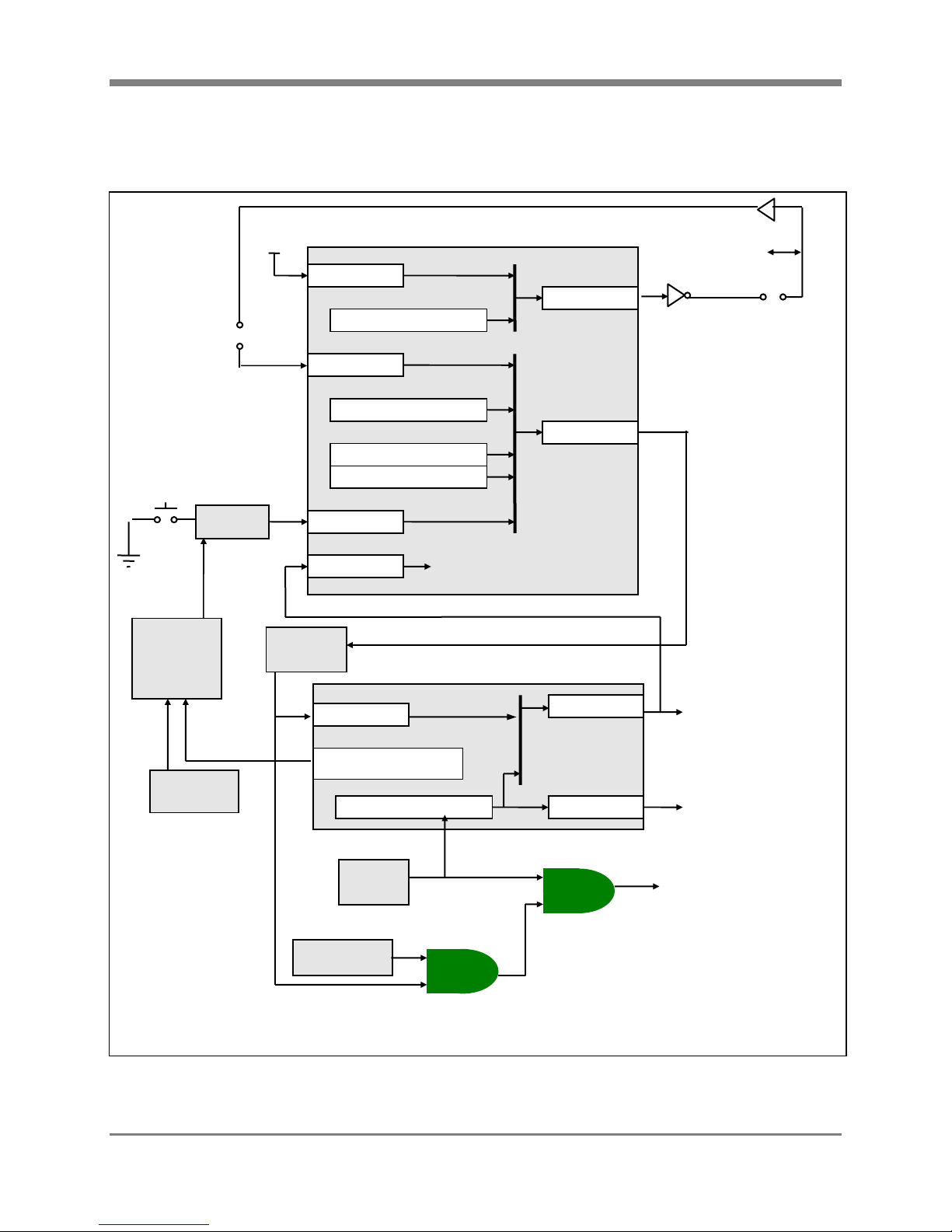
The reset circuitry is shown below:
Pull-up
JP4
Front Panel Reset Switch
+5 VDC Monitor
DS1232
PB1
Watchdog
Strobe
Open Drain
NAND Gate
VME_RESET#
MISC_CTL[SW_SYSRST]
VRSYSRST#
MISC_CTL[SW_LRST]
VCSR_SET[RESET]
VCSR_CLR[RESET]
PWRRST#
RST#
Buffer
Universe IID CA91C142D
Reset Registers,
State Machines
ICH
VMEbus
SYSRESET
VXSYSRST
JP2
LRST#
WDT_CLKEN
14.318 MHz
Clock
SYSRESET#
General Purpose Output
Re
ister’s GPIO20
Reset Control Register
Vcore
Monitor
LTC1778
3.3V Reset
PCIRST#
INIT
PWRGD_VR
PCI peripherals
Core Duo “soft” reset
Core Duo “hard” reset
Reset Circuitry
CPU-71-10 (XPD/RPD/DPD) VMEbus Core 2 Duo Processor Board – User’s Manual 13
Page 18

Chapter 3 – Hardware Description
There are eight ways to perform a hard reset of the XPD:
The DS1232 senses that the +5 VDC supply has dropped too low, asserting a PWROK signal to the ICH. This
signal resets the processor and the Chipset and, ultimately, all PCI and PCI-X peripherals. The output of the
DS1232 runs through the Universe IID (If the board is delivered without the VMEbus interface circuitry (the
XPD) this path is replaced with a bypass 0 ohm resistor).
A DS1233 monitors the on-board 3.3 VDC, regulated from the 5.0 VDC off the backplane, and provides
proper power sequencing for the CPU.
The local on-board voltage regulator for the CPU’s core voltage will g enerate a reset if its output voltage is out
of range through signal PWRGD_VR.
The front panel reset switch, PB1, is pressed, which also asserts a PWROK signal from the DS1232 and resets
the XPD.
Another VMEbus board asserts SYSRESET*, which asserts the Universe IID VRSYSRST# input and, if
Jumper SW1-1 is closed, will reset the XPD.
The SW_SYSRST bit in the MISC_CTL register of the Universe IID is set by code running on the XPD
processor. This asserts the VMEbus SYSRESET* signal if SW1-2 is closed. If SW1-1 is open the XPD can
reset the VMEbus without resetting itself.
The SW_LRST bit in the MISC_CTL register of the Universe IID is set by code running on the XPD processor.
This performs a local hard reset, via signal LRST#, of the XPD board circuitry. If SW1-2 is open LRST# will
reset the XPD without asserting a VMEbus SYSRESET* signal.
Another VMEbus master sets the RESET bit in the VCSR_SET register of the Universe IID over the VMEbus.
In this case the LRST# signals remains asserted until the RESET bit of the VCSR_CLR register of the Universe
IID is set by another VMEbus master over the VMEbus.
The Reset Control Register in the ICH can be set appropriately by code running on the XPD processor.
Let the watchdog timer time out; see Section 3.12 below.
For further information on the peripherals that play a part in the reset circuitry, refer to ICH datasheet that’s
referenced in Section 2.
3.12 Watchdog Timer Operation
The XPD’s DS1232 if the watchdog timer is enabled and times out.
The XPD’s watchdog timer is controlled by one general-purpose output line (GPIO20) that is asserted by the ICH.
The DS1232 has a strobe input pin that must see an active clock. If no clock pulse is generated to the pin within
500 milliseconds, the entire XPD board will be reset. As long as GPIO20 is high, a 14.31818 MHz clock will be
present at the strobe input.
To use the watchdog timer, drive GPIO20 low, thereby turning off the 14.31818 MHz clock to the DS1232’s strobe
input, and write a software routine that will bring GPIO20 high before 500 milliseconds elapses. GPIO20 is
controlled by bit 20 in the ICH’s GP_LVL register. GPIO20 reflects the status of bit 20: GPIO20 is high if bit 20 is
at logic 1 and it is low if bit 20 is at logic 0. GPIO20 is high at reset so the watchdog timer will only be activated
when the user drives bit 20 of the GP_LVL register low. For instructions on programming the GP_LVL register,
refer to the Intel® 6300ESB I/O Controller Hub Data Sheet from Intel Corporation, Document # 300641-002.
14 CPU-71-10 (XPD/RPD/DPD) VMEbus Core 2 Duo Processor Board – User’s Manual
Page 19
Chapter 4 – Installation
4. Installation
The following sections cover the steps necessary to configur e the XPD and install it into a VMEbus system for
single-slot operation. This chapter should be read in its entirety before proceeding with the installation.
4.1 Selectable Options
This section explains how to set up user configurable jumpers and how to install CompactFlash drives and PMC
modules.
The XPD is shipped in an antistatic bag. Be sure to observe proper handling procedures during the configuration
and installation process, to avoid damage due to electrostatic discharge (ESD).
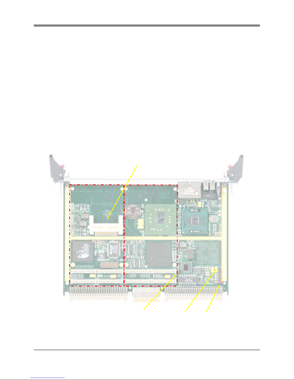
The XPD contains eight jumpers. JP3 is located near JN1 for the second PMC site. Jumpers JP1 through JP8
(minus JP3) are arranged in order as shown below:
PMC/XMC Site 1
CompactFlash Drive
PMC Site 2
CPU-71-10 (XPD/RPD/DPD) VMEbus Core 2 Duo Processor Board – User’s Manual 15
JP1JP3
JP8
Page 20
Chapter 4 – Installation
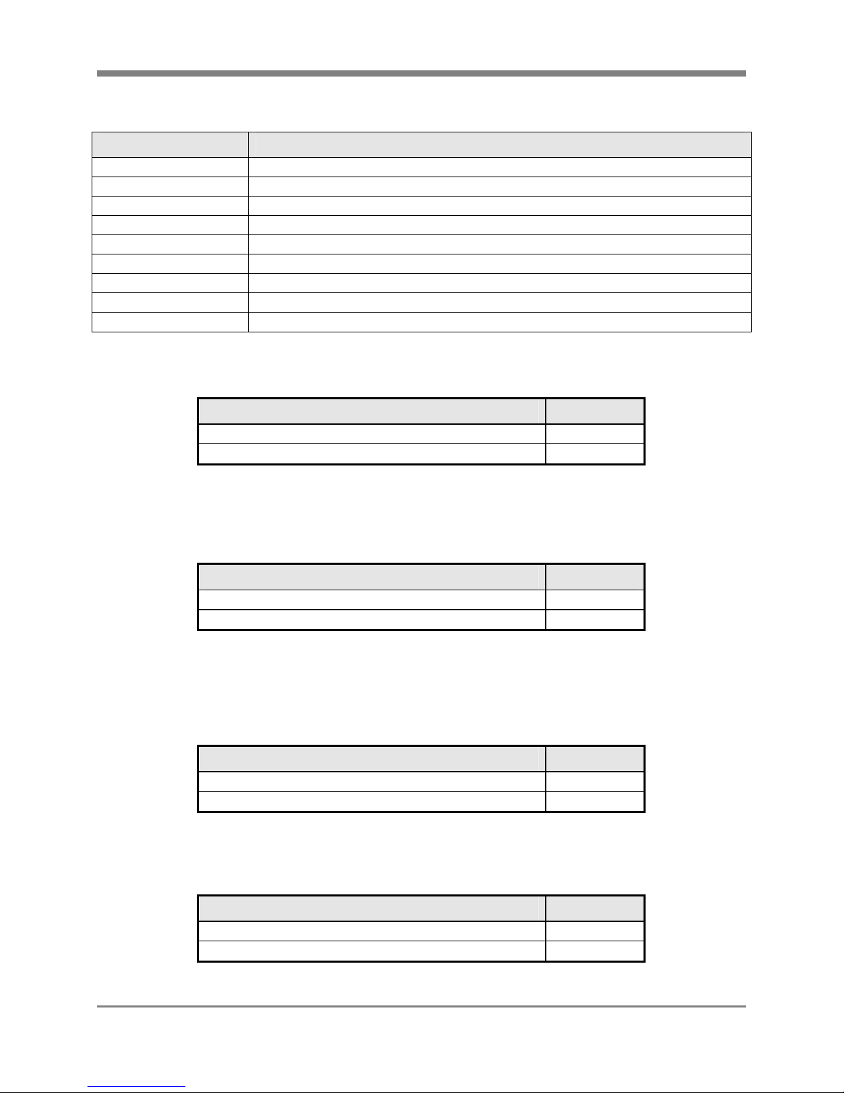
The XPD offers a number of user configurable hardware options.
Jumpers Description
JP1 VMEbus Slot 1 Controller when open
JP2 XPD drives SYSRESET to the VMEbus when closed
JP3 Determines VIO for the two PMC sites (1 – 2 for 3.3 VDC; 2 – 3 for 5.0 VDC)
JP4 XPD is reset by the VMEbus SYSRESET when closed
JP5 Close momentarily to flush RTC and NV-RAM and revert to BIOS defaults
JP6 Bit Control 1 (grounded when shunted)
JP7 Bit Control 0 (grounded when shunted)
JP8
SW2-1 through SW2-4 DDC Routing for DVI-I Interface (set at the factory)
JP2 lets an XPD SYSRESET reset the VMEbus when closed. When open, the XPD cannot drive a SYSRESET to
other modules on the VMEbus. The Universe IID only drives SYSRESET when the XPD is a Slot 1 Controller.
VMEbus SYSRESET Out Selection JP2
XPD Won’t Drive SYSRESET to the VMEbus Open
XPD Drives SYSRESET to the VMEbus Closed
MUST STAY OPEN (on-board BIOS is disabled when closed)
VMEbus SYSRESET Out Selection
When a VMEbus module occupies slot 1 of the VMEbus chassis (the slot to the extreme left), it must operate as
system controller (act as multiprocessing arbiter and generate utility bus signals). JP1 configures the VMEbus
System Controller functionality of the Universe IID, as shown below:
VMEbus System Controller JP1
Enabled Open
Disabled Closed
VMEbus System Controller Configuration
Jumper JP3 selects the VIO routed to the XPD’s two PMC modules. The VIO pins determine the signaling voltage
on the PMC modules’ PCI interface. Refer to the PMC modules’ reference manuals to ascertain the recommended
VIO. Shunting pins 1 & 2 of JP1 provides a VIO of 3.3 VDC. Shunting pins 2 & 3 routes 5 VDC to the VIO pins
on the PMC modules.
VIO Voltage Level JP3
3.3 VDC 1-2
5 VDC 2-3
Battery Voltage Supply Selection
JP4 lets VMEbus SYSRESET reset the XPD when closed. When open, a VMEbus SYSRESET from other modules
will not reset the XPD.
VMEbus SYSRESET In Selection JP4
XPD Won’t Receive SYSRESET from the VMEbus Open
XPD Receives SYSRESET from the VMEbus Closed
16 CPU-71-10 (XPD/RPD/DPD) VMEbus Core 2 Duo Processor Board – User’s Manual
VMEbus SYSRESET In Selection
Page 21
Chapter 4 – Installation
Jumper JP5 is provided for clearing the NVRAM. If BIOS parameters are modified and the XPD goes into a failure
mode, default variables can be restored by closing JP5 for roughly 15 seconds.
4.2 CompactFlash Drive Installation
The XPD supports a bootable CompactFlash Drive for booting up into an Operating System (OS) while occupying
only one slot in the VMEbus chassis. Connector J3 is a Type II CompactFlash connector and is used for this
purpose. J3 is located below PMC site 1.
4.3 PCI Mezzanine Card (PMC) Installation
The XPD supports two PMC add-on module sites that let the user expand the XPD’s local I/O with PCI Mezzanine
Cards (PMC) or PMCX (PMC modules capable of PCI-X transfers) modules. The PMCX sites are backwards
compatible and can support any modules from 32-bit PMC cards at 33 MHz to 64-bit PMCX modules at 66 MHz.
The PMCX sites on the XPD are routed from the ICH’s PCI-X bus interface which is 64 bits wide and has a
maximum clock rate of 66 MHz.
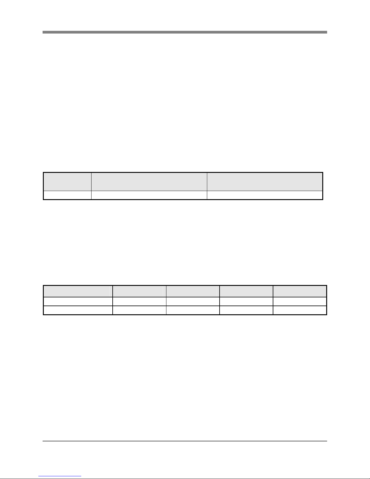
PMCX sites Available Data Rates with VIO = 5 V
(JP3 is shunted between pins 2 & 3)
Available Data Rates with VIO = 3.3 V
(JP3 is shunted between pins 1 & 2)
1 & 2 33 MHz 33 MHz and 66 MHz
The General Software BIOS will determine during startup what the status of the PCI-X bus. The BIOS monitors the
following pins that are routed to the ICH: PCIXCAP (PCX-X capable) and M66EN (66 MHz capable). The user’s
manual on your PMC(X) modules will tell you how PCIXCAP (JN1, pin 39) and M66EN (JN2, pin 47) are
configured. Since both sites share the same bus, JP3 sets the VIO voltage for both sites and the bus will only clock
as fast as the slower PMC card.
Conventionally PMC connectors have four designators: JN1 – JN4. JN1 & JN2 provide all the signals necessary for
32-bit PCI transactions, JN3 has the 32 additional data lines required for 64-bit transfers, and JN4 routes I/O off the
module for possible backplane access (see Section A for J14 to P2 and J24 to P0 backplane PMCX I/O routing).
The following table lists the reference designators used on the XPD’s PMC(X) sites:
PMCX site JN1 JN2 JN3 JN4
1 (also supports XMC) J11 J12 J13 J14 (to P2)
2 J21 J22 J23 J24 (to P0)
4.4 VMEbus Chassis Installation
Unless your VMEbus chassis features automatic daisy chaining, it will have a set of five jumpers for each slot:
Interrupt Acknowledge – IACKIN* and IACKOUT*
Bus Grant 0 – BG0IN* and BG0OUT*
Bus Grant 1 – BG1IN* and BG1OUT*
Bus Grant 2 – BG2IN* and BG2OUT*
Bus Grant 3 – BG3IN* and BG3OUT*
CPU-71-10 (XPD/RPD/DPD) VMEbus Core 2 Duo Processor Board – User’s Manual 17
Page 22

Chapter 4 – Installation
These jumpers are typically found between slots, and when configuring a VMEbus chassis, care must be taken to
correctly determine the slot affected by the jumpers (the slot to the right of the jumpers). The interrupt acknowledge
is a daisy chain from the board acknowledging the interrupt request to the boards that can issue an interrupt request.
The bus grant signals are daisy chains from the system controller, which contains the bus arbiter, to the boards that
can request the bus.
Empty VMEbus slots between boards should have all of these jumpers installed. Any slot containing the XPD
should have all of these jumpers removed. Any VMEbus slots after the last board in the chassis (that is, the board
farthest away from the system controller, which is always in slot 1) do not require these jumpers. For other boards
in the VMEbus chassis, refer to their installation instructions for their jumper requirements.
Once the VMEbus chassis jumpers are installed, insert the XPD into its designated slot. With the XPD ejector
handles inward, firmly push the XPD into the VMEbus connectors on the chassis. Tighten the screws to the outside
of the ejector handles to complete the installation of the XPD in the VMEb us chassis.
4.5 Front Panel Connectors and Reset Switch
The XPD offers front panel connections for two USB ports and two RJ45 connector for 1000BaseTX Ethernet
ports. Install all front panel cables by inserting them into the appropriate connector. COM1 and DVO/VGA cables
can be secured to the XPD by tightening their thumbscrews into the connectors’ jackscrews. USB and Ethernet
mating connectors should snap into place. Mounting hardware for the front panel connectors are isolated from the
XPD’s digital ground. They are continuous with the front panel itself that, in turn, is common with chassis ground.
The XPD contains a recessed reset switch, accessible from the front panel. To reset the XPD, press the reset switch
using a small screwdriver blade or similar implement.
The Ethernet connectors each have a pair of indicator LEDs built in. These two green LEDs offer stats on the
1000BaseTX port provided by the 82571EB Ethernet controller on the XPD.
Link – Ethernet link is established when on. This LED is to the left (or top when the XPD is held
vertically)
Activity – Ethernet data is being transmitted from or received by the XPD when on. This LED is to the
right/bottom of the Link LED.
18 CPU-71-10 (XPD/RPD/DPD) VMEbus Core 2 Duo Processor Board – User’s Manual
Page 23
Appendix A – Connector Pin-outs
A. Connector Pin-outs
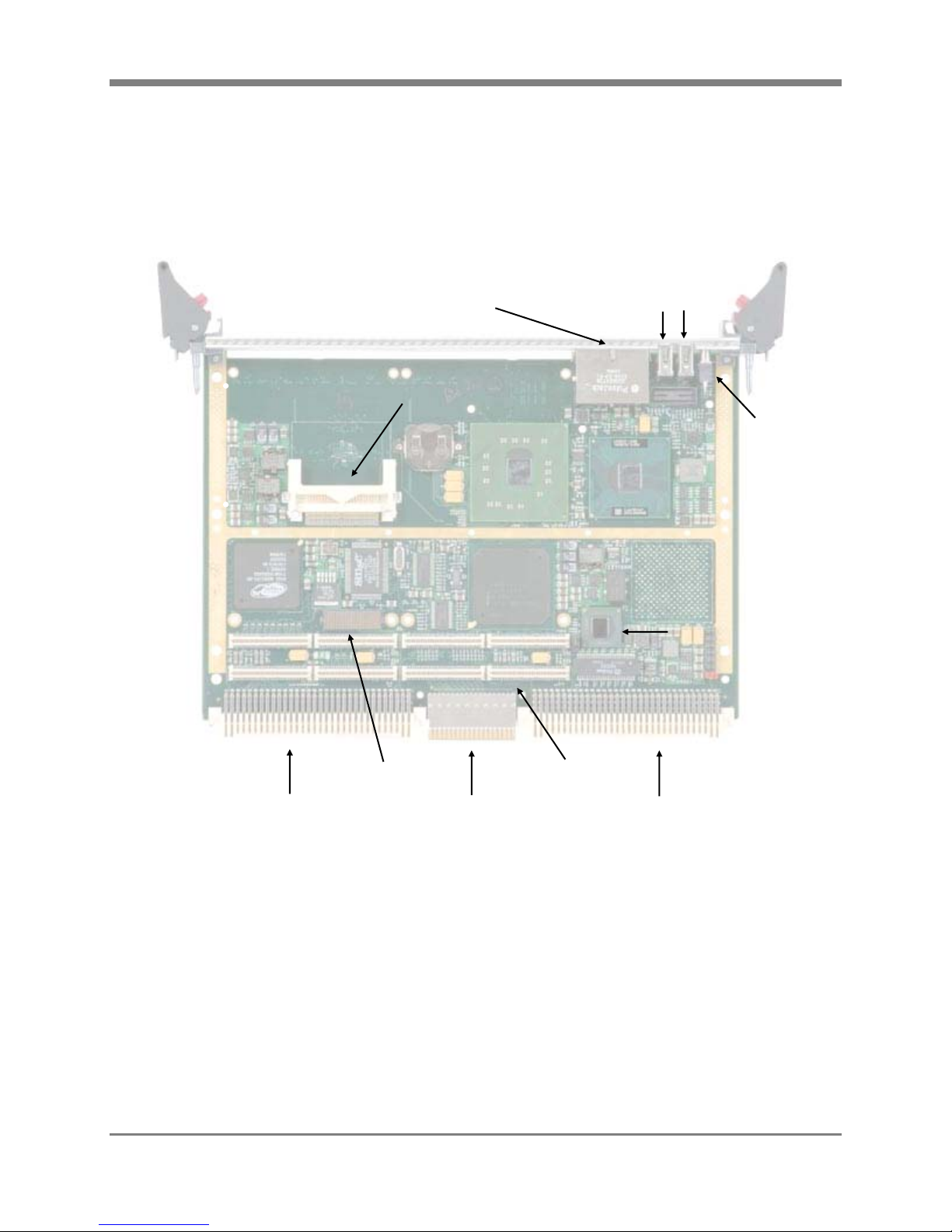
The locations of the XPD connectors are shown below. The connectors that do not go to the front panel have their
pin 1 location designated accordingly.
J13
J14
J11
J12
Two 1Gb LAN Ports - J1
CompactFlash – J3
J15
J23
J24
MCH
ICH
J21
J22
USB0/1
A B
Reset Button
Core Duo
Universe
82571EB Dual Gb LAN
VMEbus – P2
CPU-71-10 (XPD/RPD/DPD) VMEbus Core 2 Duo Processor Board – User’s Manual 19
XMC Connector
VMEbus – P0
PMC Connectors
VMEbus – P1
Page 24

Appendix A – Connector Pin-outs
A.1 Front Panel USB Connector (USB1 & USB2)
There are two USB connectors (labeled USB1 & USB2) accessible at the XPD’s front panel. Though they are
separate ports, their pin-outs are identical so the following table offers the pin-out of one connector as both.
Pin Signal Description
1 +5 VDC (via 1.1 amp self-resetting fuse F2)
2 Negative Data
3 Positive Data
4 Signal GND
5 Chassis GND
6 Chassis GND
7 Chassis GND
8 Chassis GND
USB Connectors (USB1 & USB2) – Front Panel USB Receptacles. The metal shell of the
connector goes to chassis ground.
A.2 1000BaseTX Fast Ethernet Front Panel Connector (J1)
The XPD uses a dual RJ45 connector to provide two 1000BaseTX Ethernet ports at the front panel. Though there
are two separate ports in one connector, the pin-outs are identical so the following table offers the pin-out of one
connector as both.
Pin Signal Description Signal Description
1 Port A Transmit Data + (TX+) TP0+
2 A Transmit Data - (TX-) TP03 A Receive Data + (RX+) TP1+
4 Unused TP2+
5 Unused TP26 A Receive Data - (RX-) TP17 Unused TP3+
8 Unused TP3-
1000BaseTX Fast Ethernet Connector (J1) – Front Panel RJ-45 Connector. The metal shell of the
connector goes to chassis ground.
20 CPU-71-10 (XPD/RPD/DPD) VMEbus Core 2 Duo Processor Board – User’s Manual
Page 25

Appendix A – Connector Pin-outs
A.3 CompactFlash Interface Connector (J3)
Pin Signal Pin Signal
1 GND 26 No connection
2 D3 27 D11
3 D4 28 D12
4 D5 29 D13
5 D6 30 D14
6 D7 31 D15
7 CS1# 32 CS3#
8 GND 33 No connection
9 GND 34 DIOR#
10 GND 35 DIOW#
11 GND 36 +5 VDC
12 GND 37 DIRQ (IRQ15)
13 +5 VDC 38 +5 VDC
14 GND 39 Pulled Low (master)
15 GND 40 No connection
16 GND 41 IDERESET
17 GND 42 Pulled Up to 3.3
VDC
18 DA2 43 No connection
19 DA1 44 +5 VDC
20 DA0 45 No connection
21 D0 46 Pull-up to +5 VDC
22 D1 47 D8
23 D2 48 D9
24 No connection 49 D10
25 No connection 50 GND
CompactFlash Type II Interface Connector (J3)
CPU-71-10 (XPD/RPD/DPD) VMEbus Core 2 Duo Processor Board – User’s Manual 21
Page 26

Appendix A – Connector Pin-outs
A.4 VMEbus Connectors (P1, P2, and P0)
Pin Signal Pin Signal Pin Signal Pin Signal Pin Signal
Z01 NC A01 D00 B01 BBSY* C01 D08 D01 +5 VDC
Z02 GND A02 D01 B02 BCLR* C02 D09 D02 GND
Z03 JTAG_TCK A03 D02 B03 ACFAIL* C03 D10 D03 NC
Z04 GND A04 D03 B04 BG0IN* C04 D11 D04 NC
Z05 JTAG_TDO A05 D04 B05 BG0OUT* C05 D12 D05 NC
Z06 GND A06 D05 B06 BG1IN* C06 D13 D06 NC
Z07 JTAG_TDI A07 D06 B07 BG1OUT* C07 D14 D07 NC
Z08 GND A08 D07 B08 BG2IN* C08 D15 D08 NC
Z09 JTAG_TMS A09 GND B09 BG2OUT* C09 GND D09 GAP#
Z10 GND A10 SYSCLK B10 BG3IN* C10 SYSFAIL* D10 GA0#
Z11 NC A11 GND B11 BG3OUT* C11 BERR* D11 GA1#
Z12 GND A12 DS1* B12 BR0* C12 SYSRST* D12 NC
Z13 NC A13 DS0* B13 BR1* C13 LWORD* D13 GA2#
Z14 GND A14 WRITE* B14 BR2* C14 AM5 D14 NC
Z15 NC A15 GND B15 BR3* C15 A23 D15 GA3#
Z16 GND A16 DTACK* B16 AM0 C16 A22 D16 NC
Z17 NC A17 GND B17 AM1 C17 A21 D17 GA4#
Z18 GND A18 AS* B18 AM2 C18 A20 D18 NC
Z19 NC A19 GND B19 AM3 C19 A19 D19 NC
Z20 GND A20 IACK* B20 GND C20 A18 D20 NC
Z21 NC A21 IACKIN* B21 No connection (NC) C21 A17 D21 NC
Z22 GND A22 IACKOUT* B22 No connection (NC) C22 A16 D22 NC
Z23 NC A23 AM4 B23 GND C23 A15 D23 NC
Z24 GND A24 A07 B24 IRQ7* C24 A14 D24 NC
Z25 NC A25 A06 B25 IRQ6* C25 A13 D25 NC
Z26 GND A26 A05 B26 IRQ5* C26 A12 D26 NC
Z27 NC A27 A04 B27 IRQ4* C27 A11 D27 NC
Z28 GND A28 A03 B28 IRQ3* C28 A10 D28 NC
Z29 NC A29 A02 B29 IRQ2* C29 A09 D29 NC
Z30 GND A30 A01 B30 IRQ1* C30 A08 D30 NC
Z31 NC A31 -12VDC/NC B31 +5 VDC Standby C31 +12VDC/NC D31 GND
Z32 GND A32 +5 VDC B32 +5 VDC C32 +5 VDC D32 +5 VDC
VMEbus Connector (P1) – DIN 41612 96-pin (3 rows x 32 pins)
22 CPU-71-10 (XPD/RPD/DPD) VMEbus Core 2 Duo Processor Board – User’s Manual
Page 27

Appendix A – Connector Pin-outs
The XPD routes the primary IDE interface to the P2 connector’s a and c rows while the middle row, row b, is used
for the VMEbus’ extended address and data bus. The IDE pins are in blue font.
Other I/O routed out through the P2 connector are two USB 2.0 ports, PS/2 Mouse & Keyboard, and four RS232
serial ports: two have full handshaking while the other two are just two-wire interfaces.
I/O pins from JN4 (connector P14) of the PMCX module are routed to rows d and z.
Pin Signal Pin Signal Pin Signal Pin Signal Pin Signal
Z01 P14-2 A01 PDD7 B01 +5 VDC C01 PDD8 D01 P14-1
Z02 GND A02 PDD6 B02 GND C02 PDD9 D02 P14-3
Z03 P14-5 A03 PDD5 B03 No Connect C03 PDD10 D03 P14-4
Z04 GND A04 PDD4 B04 A24 C04 PDD11 D04 P14-6
Z05 P14-8 A05 PDD3 B05 A25 C05 PDD12 D05 P14-7
Z06 GND A06 PDD2 B06 A26 C06 PDD13 D06 P14-9
Z07 P14-11 A07 PDD1 B07 A27 C07 PDD14 D07 P14-10
Z08 GND A08 PDD0 B08 A28 C08 PDD15 D08 P14-12
Z09 P14-14 A09 PIORDY B09 A29 C09 PDDREQ D09 P14-13
Z10 GND A10 PDDACK# B10 A30 C10 PDIOW# D10 P14-15
Z11 P14-17 A11 IRQ14 B11 A31 C11 PDIOR# D11 P14-16
Z12 GND A12 PDA1 B12 GND C12 PDA2 D12 P14-18
Z13 P14-20 A13 PDA0 B13 +5 VDC C13 PDCS3# D13 P14-19
Z14 GND A14 PDCS1# B14 D16 C14 USB_3N D14 P14-21
Z15 P14-23 A15 BIT_OUT1 B15 D17 C15 USB_3P D15 P14-22
Z16 GND A16 BIT_OUT0 B16 D18 C16 PRI_RST# D16 P14-24
Z17 P14-26 A17 BIT_CNTRL1 B17 D19 C17 USB_2N C17 P14-25
Z18 GND A18 BIT_CNTRL0 B18 D20 C18 USB_2P D18 P14-27
Z19 P14-29 A19 EXT_RST# B19 D21 C19 USB_V D19 P14-28
Z20 GND A20 +5 VDC B20 D22 C20 GND D20 P14-30
Z21 P14-32 A21 COM1-DCD B21 D23 C21 COM2-DCD D21 P14-31
Z22 GND A22 COM1-DSR B22 GND C22 COM2-DSR D22 P14-33
Z23 P14-35 A23 COM1-RxD B23 D24 C23 COM2-RxD D23 P14-34
Z24 GND A24 COM1-RTS B24 D25 C24 COM2-RTS D24 P14-36
Z25 P14-38 A25 COM1-TxD B25 D26 C25 COM2-TxD D25 P14-37
Z26 GND A26 COM1-CTS B26 D27 C26 COM2-CTS D26 P14-39
Z27 P14-41 A27 COM1-DTR B27 D28 C27 COM2-DTR D27 P14-40
Z28 GND A28 COM1-RI B28 D29 C28 COM2-RI D28 P14-42
Z29 P14-44 A29 COM3-RxD B29 D30 C29 COM4-RxD D29 P14-43
Z30 GND A30 COM3-TxD B30 D31 C30 COM4-TxD D30 P14-45
Z31 P14-46 A31 KBDATA B31 GND C31 MDATA D31 GND
Z32 GND A32 KBCLK B32 +5 VDC C32 MCLK D32 +5 VDC
VMEbus Connector (P2) – 160-pin (5 rows x 32 pins)
CPU-71-10 (XPD/RPD/DPD) VMEbus Core 2 Duo Processor Board – User’s Manual 23
Page 28

Appendix A – Connector Pin-outs
Connector P0 routes two Gb Ethernet ports (in compliance with VITA 31.1), a VGA interface, and two Serial ATA
ports.
The two Gb Ethernet ports occupy rows 2 through 5. To follow Vita 31.1 to the letter, rows 1 & 6 are all no
connects and pins C02 through C05 are grounded. The XPD can comply to Vita 31.1 by the appropriate use of 0
ohm resistors but in the pin-out below these pins are used for two SATA ports and the VGA port.
Pin Signal Pin Signal Pin Signal Pin Signal Pin Signal
SATA1_TXN
A01
LPa_DA+
A02
LPa_DB+
A03
LPb_DA+
A04
LPb_DB+
A05
SATA1_RXN
A06
PIO5
A07
PIO10
A08
PIO15
A09
PIO20
A10
PIO25
A11
PIO30
A12
PIO35
A13
PIO40
A14
PIO45
A15
PIO50
A16
PIO55
A17
PIO60
A18
VGA_ddcclk
A19
VME64 Extensions Bus Connector (P0) for XPD, Rev A (PWB D010 6065 001) – Row F is grounded
B01
B02
B03
B04
B05
B06
B07
B08
B09
B10
B11
B12
B13
B14
B15
B16
B17
B18
B19
SATA1_TXP
LPa_DALPa_DBLPb_DALPb_DB-
SATA1_RXP
PIO4
PIO9
PIO14
PIO19
PIO24
PIO29
PIO34
PIO39
PIO44
PIO49
PIO54
PIO59
PIO64
C01
C02
C03
C04
C05
C06
C07
C08
C09
C10
C11
C12
C13
C14
C15
C16
C17
C18
C19
VGA_Red
VGA_Green
VGA_Blue
VGA_HSYNC
VGA_VSYNC
VGA_ddcdata
PIO3
PIO8
PIO13
PIO18
PIO23
PIO28
PIO33
PIO38
PIO43
PIO48
PIO53
PIO58
PIO63
D01
D02
D03
D04
D05
D06
D07
D08
D09
D10
D11
D12
D13
D14
D15
D16
D17
D18
D19
SATA0_TXN
LPa_DC+
LPa_DD+
LPb_DC+
LPb_DD+
SATA0_RXN
PIO2
PIO7
PIO12
PIO17
PIO22
PIO27
PIO32
PIO37
PIO42
PIO47
PIO52
PIO57
PIO62
E01
E02
E03
E04
E05
E06
E07
E08
E09
E10
E11
E12
E13
E14
E15
E16
E17
E18
E19
SATA0_TXP
LPa_DCLPa_DDLPb_DCLPb_DD-
SATA0_RXP
PIO1
PIO6
PIO11
PIO16
PIO21
PIO26
PIO31
PIO36
PIO41
PIO46
PIO51
PIO56
PIO61
24 CPU-71-10 (XPD/RPD/DPD) VMEbus Core 2 Duo Processor Board – User’s Manual
Page 29

Appendix A – Connector Pin-outs
A.5 PCI-X Mezzanine Card Connectors (JN1, JN2, JN3, and JN4) and the XMC connector (J15)
This section has the pin-outs for all four PMC connectors. There are two PMC sites. Their pinouts are largely
identical. When signals differ between the two PMC sites, red font will be used for PMC Site 1 (see the photo at the
beginning of Section 4 of this User’s Manual) and blue font will be used for PMC Site 2. JN4 pinouts for the two
different sites, I/O connectors where the pins are routed to P2 & P0 respectively, are completely different for the
two sites so these pinouts will be provided separately.
Pin Signal Pin Signal
1 5.6K pull-down 2 -12 VDC
3 GND 4 PX_PIRQ0#/PX_PIRQ1#
5 PX_PIRQ1#/PX_PIRQ2# 6 PX_PIRQ2#/PX_PIRQ3#
7 No connection 8 +5 VDC
9 PX_PIRQ3#/PX_PIRQ0# 10 No connection
11 GND 12 No connection
13 PMC1CLK/PMC1CLK 14 GND
15 GND 16 GNT0#/GNT1#
17 REQ0#/REQ1# 18 +5 VDC
19 VI/O from JP3 20 AD31
21 AD28 22 AD27
23 AD25 24 GND
25 GND 26 C/BE3#
27 AD22 28 AD21
29 AD19 30 +5 VDC
31 VI/O from JP3 32 AD17
33 FRAME# 34 GND
35 GND 36 IRDY#
37 DEVSEL# 38 +5 VDC
39 PCIXCAP 40 LOCK#
41 No connection 42 No connection
43 PAR 44 GND
45 VI/O from JP3 46 AD15
47 AD12 48 AD11
49 AD9 50 +5 VDC
51 GND 52 C/BE0#
53 AD6 54 AD5
55 AD4 56 GND
57 VI/O from JP3 58 AD3
59 AD2 60 AD1
61 AD0 62 +5 VDC
63 GND 64 REQ64#
PCI-X Mezzanine Card (PMCX) Connector (JN1) – Molex 71439-0164
VIO is jumper selectable through JP3 (please see Section 4.1).
CPU-71-10 (XPD/RPD/DPD) VMEbus Core 2 Duo Processor Board – User’s Manual 25
Page 30

Appendix A – Connector Pin-outs
Pin Signal Pin Signal
1 +12 VDC 2 TRST (pulled down)
3 TMS (pulled up) 4 No connection
5 TDI (pulled up) 6 GND
7 GND 8 No connection
9 No connection 10 No connection
11 +3.3 VDC 12 +3.3 VDC
13 PCI RST# 14 GND
15 +3.3 VDC 16 GND
17 No connection 18 GND
19 AD30 20 AD29
21 GND 22 AD26
23 AD24 24 +3.3 VDC
25 (IDSEL) AD17/AD18 26 AD23
27 +3.3 VDC 28 AD20
29 AD18 30 GND
31 AD16 32 C/BE2#
33 GND 34 No connection
35 TRDY# 36 +3.3 VDC
37 GND 38 STOP#
39 PERR# 40 GND
41 +3.3 VDC 42 SERR#
43 C/BE1# 44 GND
45 AD14 46 AD13
47 M66EN 48 AD10
49 AD8 50 +3.3 VDC
51 AD7 52 No connection
53 +3.3 VDC 54 No connection
55 No connection 56 GND
57 No connection 58 No connection
59 GND 60 No connection
61 ACK64# 62 +3.3 VDC
63 GND 64 No connection
PCI-X Mezzanine Card (PMCX) Connector (JN2) – Molex 71439-0164
26 CPU-71-10 (XPD/RPD/DPD) VMEbus Core 2 Duo Processor Board – User’s Manual
Page 31

Appendix A – Connector Pin-outs
Pin Signal Pin Signal
1 No connection 2 GND
3 GND 4 C/BE7#
5 C/BE6# 6 C/BE5#
7 C/BE4# 8 GND
9 VIO 10 PAR64
11 AD63 12 AD62
13 AD61 14 GND
15 GND 16 AD60
17 AD59 18 AD58
19 AD57 20 GND
21 VIO 22 AD56
23 AD55 24 AD54
25 AD53 26 GND
27 GND 28 AD52
29 AD51 30 AD50
31 AD49 32 GND
33 GND 34 AD48
35 AD47 36 AD46
37 AD45 38 GND
39 VIO 40 AD44
41 AD43 42 AD42
43 AD41 44 GND
45 GND 46 AD40
47 AD39 48 AD38
49 AD37 50 GND
51 GND 52 AD36
53 AD35 54 AD34
55 AD33 56 GND
57 VIO 58 AD32
59 No connection 60 No connection
61 No connection 62 GND
63 GND 64 No connection
PCI-X Mezzanine Card (PMCX) Connector (JN3) – Molex 71439-0164
CPU-71-10 (XPD/RPD/DPD) VMEbus Core 2 Duo Processor Board – User’s Manual 27
Page 32

Appendix A – Connector Pin-outs
Pin Signal Pin Signal
1 D1 2 Z1
3 D2 4 D3
5 Z3 6 D4
7 D5 8 Z5
9 D6 10 D7
11 Z7 12 D8
13 D9 14 Z9
15 D10 16 D11
17 Z11 18 D12
19 D13 20 Z13
21 D14 22 D15
23 Z15 24 D16
25 D17 26 Z17
27 D18 28 D19
29 Z19 30 D20
31 D21 32 Z21
33 D22 34 D23
35 Z23 36 D24
37 D25 38 Z25
39 D26 40 D27
41 Z27 42 D28
43 D29 44 Z29
45 D30 46 Z31
47 No connection 48 No connection
49 No connection 50 No connection
51 No connection 52 No connection
53 No connection 54 No connection
55 No connection 56 No connection
57 No connection 58 No connection
59 No connection 60 No connection
61 No connection 62 No connection
63 No connection 64 No connection
PCI-X Mezzanine Card (PMCX) Site #1 Connector (J14) – Molex 71439-0164
J14 is the JN4 I/O connector for PMC Site #1. These lines will be routed to the D & Z rows of the P2 backplane
connector.
28 CPU-71-10 (XPD/RPD/DPD) VMEbus Core 2 Duo Processor Board – User’s Manual
Page 33

Appendix A – Connector Pin-outs
Pin Signal Pin Signal
1 E7 2 D7
3 C7 4 B7
5 A7 6 E8
7 D8 8 C8
9 B8 10 A8
11 E9 12 D9
13 C9 14 B9
15 A9 16 E10
17 D10 18 C10
19 B10 20 A10
21 E11 22 D11
23 C11 24 B11
25 A11 26 E12
27 D12 28 C12
29 B12 30 A12
31 E13 32 D13
33 C13 34 B13
35 A13 36 E14
37 D14 38 C14
39 B14 40 A14
41 E15 42 D15
43 C15 44 B15
45 A15 46 E16
47 D16 48 C16
49 B16 50 A16
51 E17 52 D17
53 C17 54 B17
55 A17 56 E18
57 D18 58 C18
59 B18 60 A18
61 E19 62 D19
63 C19 64 B19
PCI-X Mezzanine Card (PMCX) Site #2 Connector (J24) – Molex 71439-0164
J24 is the JN4 I/O connector for PMC Site #2. These lines will be routed to the pins shown for the P0 backplane
connector.
CPU-71-10 (XPD/RPD/DPD) VMEbus Core 2 Duo Processor Board – User’s Manual 29
Page 34

Appendix A – Connector Pin-outs
Following is the pinout for the XMC connector associated with PMC/XMC Site #1. The XMC site routes x8 PCI
Express to the mezzanine card.
Pin Column A Column B Column C Column D Column E Column F
1 PETp0B PETn0B
2
Ground Ground TRST# pulled low Ground Ground PCI_RST#
3 PETp2B PETn2B
4
Ground Ground TCK pulled low Ground Ground No Connect
5 PETp4B PETn4B
6
Ground Ground TMS pulled high Ground Ground 12 VDC
7 PETp6B PETn6B
8
9
10
Ground Ground TDI pulled high Ground Ground -12 VDC
No Connect No Connect No Connect No Connect No Connect 5 VDC
Ground Ground No Connect Ground Ground Ground
11 PERp0B PERn0B
12
Ground Ground Ground Ground Ground No Connect
13 PERp2B PERn2B
14
Ground Ground Ground Ground Ground No Connect
15 PERp4B PERn4B
16
Ground Ground No Connect Ground Ground No Connect
17 PERp6B PERn6B
18
19
Ground Ground No Connect Ground Ground No Connect
CLK100P_XMC CLK100N_XMC No Connect No Connect No Connect No Connect
3.3 VDC
3.3 VDC
3.3 VDC
3.3 VDC
No Connect
3.3 VDC
No Connect
No Connect
PETp1B PETn1B
PETp3B PETn3B
PETp5B PETn5B
PETp7B PETn7B
PERp1B PERn1B
PERp3B PERn3B
PERp5B PERn5B
PERp7B PERn7B
XMC Bus Connector (J15) for XPD, Rev A (PWB D010 6065 001)
5 VDC
5 VDC
5 VDC
5 VDC
5 VDC
5 VDC
5 VDC
No Connect
30 CPU-71-10 (XPD/RPD/DPD) VMEbus Core 2 Duo Processor Board – User’s Manual
Page 35
Appendix B – BIOS & Setup
B. BIOS & Setup
The DPD uses General Software’s Embedded BIOS with StrongFrame™ Technology, Rev 6.The BIOS is
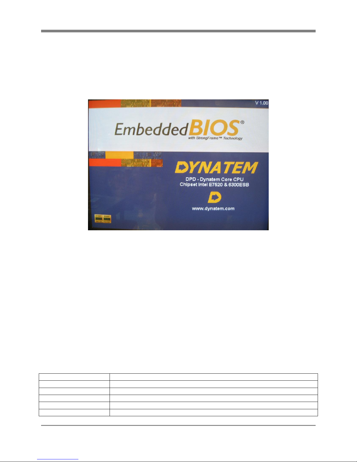
configured with the System Setup Utility, accessible from the Preboot Menu. This photo shows the initial splash
screen that is displayed after powering up the system as the BIOS runs through the Power On Self Test (POST).
When your system is powered on, Embedded BIOS tests and initializes the hardware and programs the chipset and
other peripheral components.
To enter the Setup mode, please press the delete <Del> key on your keyboard after powering up your system,
during POST.
B.1 Redirecting to a Serial Port
Setup may be run from the main keyboard and video display or from a terminal emulator program running on a host
computer connected to the system through a serial cable. To use a serial port, connect a dumb terminal or a PC
running a terminal emulation utility like Hyperterminal to COM1 via a null modem. Next, set the communications
parameters of the host’s terminal program to 115Kbaud. Other parameters are 8-bit, no parity, and one stop bit. Do
not enable XON/XOFF or hardware flow control.
With this link set up, power on the system. Press ^C a few times on your dumb terminal or your PC as the system
boots. POST will redirect to the serial console, and after it has completed its early stages, it will start the preboot
menu.
B.2 Setup Menus
The standard Embedded BIOS setup menus are described below in the order they generally appear in the menuing
system (Dynatem cannot vouch for support for all BIOS functions described in the subsequent sections):
Main Display main system components and allow editing of date and time.
Exit Save changes and exit, discard changes and exit, or restore factory default settings.
Boot Configure boot actions and boot devices.
POST Configure POST.
PnP Configure Plug-n-Play for non-ACPI OSes.
SIO Configure Super I/O devices such as serial ports and parallel ports.
CPU-71-10 (XPD/RPD/DPD) VMEbus Core 2 Duo Processor Board – User’s Manual 31
Page 36

Appendix B – BIOS & Setup
Features Enable and disable system BIOS features like ACPI, APM, PnP, MP, quick boot, and
the splash screen.
Firmbase Configure Firmbase Technology and the features that use it, such as USB keyboard
and mouse support (commonly, USB HID), boot from USB (commonly, USB Boot),
and applications such as high availability, boot security (not user security, but chainof-trust security), and network-based remote access.
Misc Configure miscellaneous BIOS settings that do not fall into any other category.
Shadowing Configure chipset shadow RAM regions.
Security Configure which BIOS features require user authentication before they perform their
functions
CUI Configure the layout and coloring of the Common User Interface (CUI) display
engine that supports preboot applications.
Chipset Configure any chipset-specific parameters, such as memory, CPU, and bus timing,
and availability of chipset-specific features such as TFT support. Highly platformspecific and entirely up to the OEM’s implementation.
B.3 Navigating Setup Menus and Fields
Navigation (moving your cursor around, selecting items, and changing them) is easy in theSetup system. The
following chart is a helpful user reference:
UP key (also ^E) Move the cursor to the line above, scrolling the window as necessary.
DOWN key (also ^X) Move the cursor to the line below, scrolling the window as necessary.
LEFT key Go back to the menu to the left of the currently-displayed menu in the menu bar.
RIGHT key Go forward to the menu to the right of the currently-displayed menu in the menu bar.
PGUP key Move the cursor up several lines (a full window’s worth), scrolling the window as
necessary.
PGDN key Move the cursor down several lines (a full window’s worth), scrolling the window as
necessary.
HOME key Move the cursor to the first configurable field in the current menu, scrolling the
window as necessary.
END key Move the cursor to the last configurable field in the current menu, scrolling the
window as necessary.
ESC key Exit the Setup system, discarding all changes(except date/time changes, which take
place on-the-fly.)
TAB key Move the cursor down to the next configurable field.
Shift-TAB key (backtab) Move the cursor up to the last configurable field.
+ key Toggle an Enable/Disable field, or increase a numeric field’s value.
- key Toggle an Enable/Disable field, or decrease a numeric field’s value.
SPACE key Toggle an Enable/Disable field.
BKSP key Reset an Enable/Disable or multiple-choice field, or back-up in numeric or string
fields.
Digits (0-9) Used to enter numeric parameters.
Alphabetic (A-Z, a-z) Used to enter text data on ASCII fields such as email addresses.
Special symbols
(!@#$%^&*_-+={}[], etc.)
The basic idea when using the Setup system is to navigate to the menus containing fields you want to review, and
change those fields as desired. When your settings are complete, navigate to the EXIT menu, and select “Save
Settings and Restart”. This causes the settings to be stored in nonvolatile memory in the system, and the system will
reboot so that POST can configure itself with the new settings.
After rebooting it may be desirable to reenter the Setup system as necessary to adjust settings as necessary.
Used to enter special text on ASCII fields that permit these characters.
32 CPU-71-10 (XPD/RPD/DPD) VMEbus Core 2 Duo Processor Board – User’s Manual
Page 37
Appendix B – BIOS & Setup
Once the system boots, the Setup system cannot be entered; this is because the memory used by the BIOS
configuration manager is deallocated by the system BIOS, so that it can be used by the OS when it boots. To reenter
the Setup system after boot, simply reset the system or power off and power back on.
B.4 Main Setup Menu
The first menu always showing in the Setup system is the Main menu (unless disabled by the
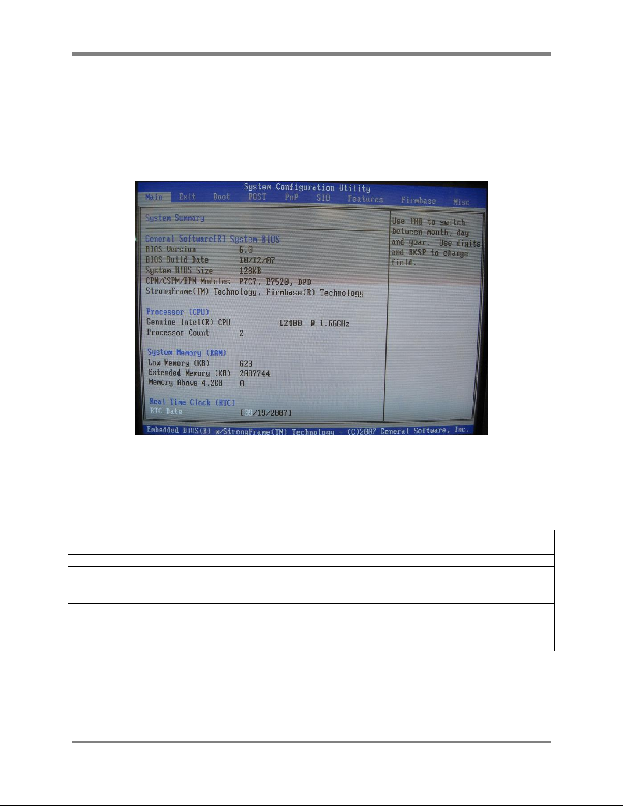
OEM.) This menu is shown in Figure 3.1 below.
The Main menu provides a system summary about the BIOS, processor, system memory, date and time, and any
other items configured by the OEM. The BIOS information is obtained by Setup from the internal system BIOS
build itself; this information is useful when obtaining support for your system.
PLEASE CALL Dynatem at (800)543-2830 FOR BIOS SUPPORT; DO NOT CALL GENERAL SOFTWARE
DIRECTLY.
BIOS Version Indicates the major and minor core architecture versions (6.x, where x is a number
from 0 to 999.)
BIOS Build Date Date in MM/DD/YY format on which Dynatem built the system BIOS binary file.
System BIOS Size Size of BIOS exposed in low memory below the 1MB boundary. Commonly, 128KB
would mean that the BIOS is visible in the address space from E000:0000 to
F000:FFFF.
CPM/CSPM/BPM
Modules
Indicates the names of the key architectural modules used to create the system BIOS
binary file. The CPM module provides the CPU family support; the CSPM module
provides the northbridge support; and the BPM module provides the board-level
support.
The CPU information is normally obtained by querying the Processor Brand String in the CPU’s MSRs; the method
used to achieve this is beyond the scope of this document.
CPU-71-10 (XPD/RPD/DPD) VMEbus Core 2 Duo Processor Board – User’s Manual 33
Page 38
Appendix B – BIOS & Setup
The system memory information does not describe physical RAM; rather it describes the RAM as configured,
subtracting RAM used for System Management Mode, Shadowing, Video buffers, and other uses. This provides
realistic values about how much memory is actually available to operating systems and applications.
The Real Time Clock fields are editable with keystrokes. To navigate through the MM/DD/YYYY and HH:MM:SS
fields, use the TAB and BACKTAB keys. The hours are normally specified in military time; thus 13 means 1pm, or
one hour after noon, whereas 01 means 1am, or one hour after midnight. When the cursor leaves RTC fields, they
either affect the battery-backed RTC right away, allowing the system to continue with your new settings, or
they revert back to old values if the new values are not valid entries.
B.5 Exit Setup Menu
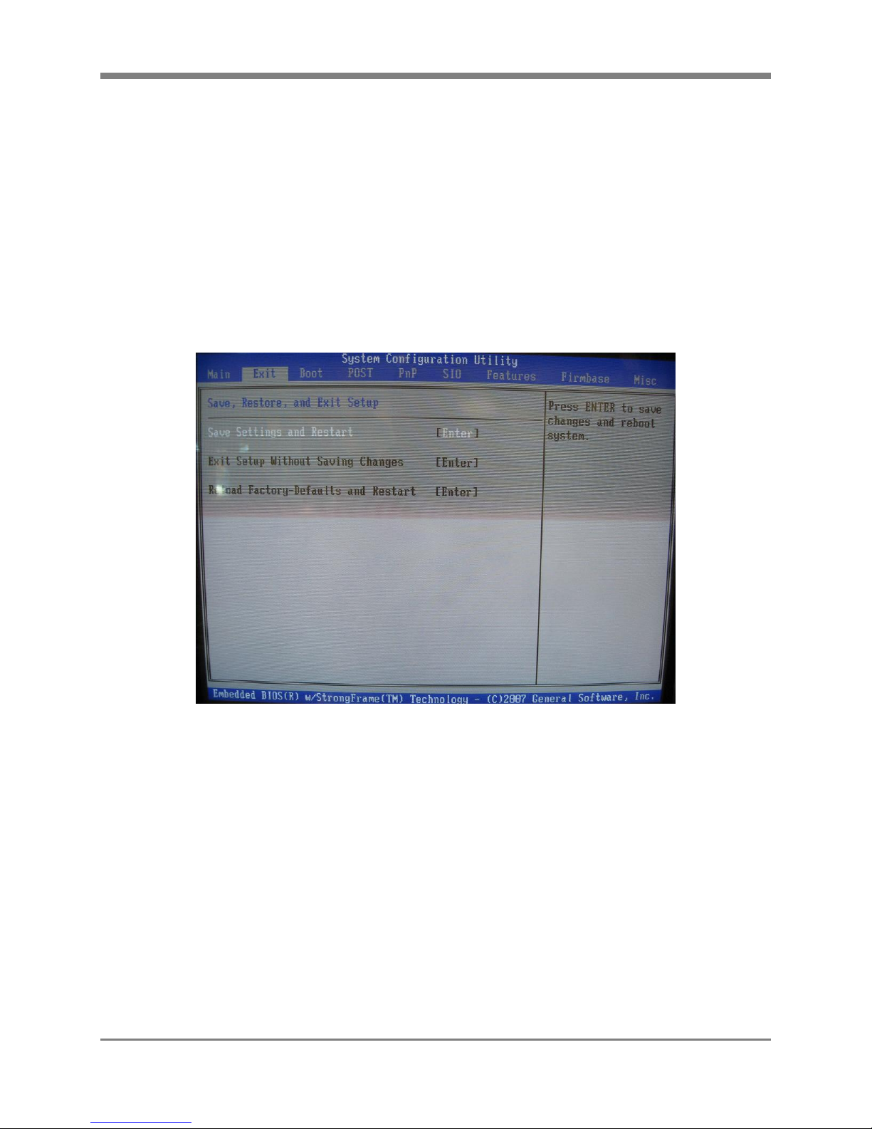
The Exit menu provides methods for saving changes made in other menus, discarding changes,
or reloading the standard system settings. This menu is shown in Figure 3.2 below.
To select any of these options, position the cursor over the option and press the ENTER key.
Pressing the ESC key at any time within the Setup system is equivalent to requesting “Exit Setup
Without Saving Changes.”
34 CPU-71-10 (XPD/RPD/DPD) VMEbus Core 2 Duo Processor Board – User’s Manual
Page 39
Appendix B – BIOS & Setup
B.6 Boot Setup Menu
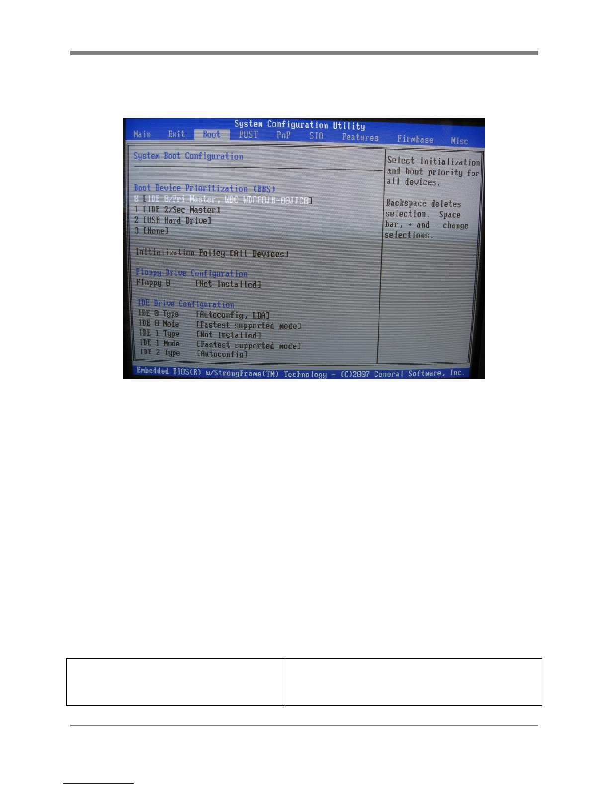
The Boot menu allows the system’s boot actions and boot devices to be configured. This menu is shown here:
The BBS portion of this menu lists the devices and activities to be performed in the or der in which they appear in
the list. When the BIOS completes POST, it follows this list, attempting to process each item. Some items are
drives, such as an ATA/IDE drive, or a USB hard disk, or CDROM.
The ordering of the drives in the BBS list controls the BIOS in several ways. First, it is the list of drives that is
scanned and assigned BIOS unit numbers for DOS (for example 80h, 81h, 83h, and so on for hard drives). If a
drive on the list is not plugged in or working properly, the BIOS moves on to the next drive, skipping the
inoperative one.
Second, once the drives in the list have been verified, POST attempts to boot from them in that order as well. Drives
without bootable partitions might be configured, but skipped over in the boot phase, so that other drives on the list
become candidates for booting the OS.
The BBS list also contains other boot actions, such as boot from network cards and PCI slots, as well as special
BIOS boot actions like “Boot EFI”, “Boot Windows CE”, or even “Boot Debugger”. When deciding what boot
action to do first and then next in succession, POST first scans all the drives in the list to verify they are present and
operating properly (as described earlier in this section) and then goes down the list and tries to perform the actions
in order. During this boot phase, if the list item is a drive, an attempt is made to boot from the boot record of that
drive. If the list item is a device like a network card or PCI slot, an attempt is made to boot from that device. If the
list item is a software item like “Boot Debugger”, then it performs that action, and when that action completes, it
moves on to the next item in the BBS list.
The table that follows lists the set of standard boot action items:
“drive name” – The system BIOS may list the
drive’s name in a generic sense (i.e., “USB Hard
Drive”) if the drive has not been detected yet, or the
Boot from the MBR/PBR of the named BIOSaware IPL
drive (BAID). The drive may be Legacy Floppy, PATA,
SATA, Compact Flash, or a USB drive.
drive’s full manufacturing name and serial number
CPU-71-10 (XPD/RPD/DPD) VMEbus Core 2 Duo Processor Board – User’s Manual 35
Page 40

Appendix B – BIOS & Setup
(if detected.)
IDE0/Primary Master Primary Master PATA drive or SATA mapping by the chipset, routed
to the backplane via P2.
IDE1/Primary Slave Primary Slave PATA drive or SATA mapping by the
chipset, routed to the backplane via P2.
IDE2/Secondary Master Secondary Master PATA drive or SATA mapping by the
chipset, routed to on-baord CompactFlash
IDE CDROM First detected IDE CDROM.
USB Floppy Drive First detected USB floppy drive.
USB Hard Drive First detected USB hard drive.
USB CDROM Drive First detected USB CDROM.
Enter Board Information Browser Invoke HTML Browser on 0.HTM in ROM.
Enter BIOS Setup Screen Invoke System Setup Utility in ROM.
Enter BIOS Debugger Invoke BIOS debugger in ROM.
Reboot System Restart system.
Power Off System Invoke S5 state, powering off system.
PCI Slot [n] Boot from device in PCI Slot ‘n’.
Network Boot from any network adapter.
SCSI Boot from external SCSI device (on PMC/XMC card).
Boot EFI Binary Boot EFI kernel from ROM or disk, depending on the EFI
source setting in the Features menu. If disk is selected, then
the BIOS searches all the configured disks in the system in
the order they appear in the BBS list, attempting to load
EFILDR.BIN from the root directory in the FAT file system
located on those drives.
Boot Windows CE Image Boot Windows CE kernel from disk. The BIOS searches all
the configured disks in the system in the order they appear in
the BBS list, attempting to load NK.BIN from the root
directory in the FAT file system located on those drives.
Boot Graphical Desktop Boot Firmbase GUI supporting graphical Firmbase
applications as well as booting DOS in a graphical window.
For applications requiring instant-on functionality even when
the OS is not available or is still loading.
The photograph above shows a common setup of the BBS list for desktop applications. In this example, the first
boot device is theWestern Digital IDE hard drive (WDC WD800JB-00JJC0) connected to the target as a Primary
Master IDE drive. The second boot device is the Secondary Master and this is the on-board CompactFlash. The
third device is a USB Hard Drive. A fourth boot device, “None”, is a placeholder that is simply used to add more
entries in the setup screen; “None” is not actually executed by POST as a boot action item.
In addition to the BBS boot device list, there are two more sections in the BOOT menu; namely, the Floppy Drive
Configuration and IDE Drive Configuration sections. Both of these sections tell the BIOS what kind of equipment is
connected to the motherboard but the floppy drive interface has not been implemented so please ignore this and
leave it as “Not Installed”. Similarly, the IDE Drive Configuration section describes the type of hard drive
equipment that is connected to the motherboard, including the cable type. IDE drives, or actually more properly
Parallel ATA (PATA) drives, are connected to the motherboard with a flat cable with either 40 or 80 wires running
in parallel (hence, Parallel ATA, as opposed to Serial ATA.) The 40-pin connector supports speeds up to UDMA2,
whereas 80-pin cables are needed for higher transfer rates to eliminate noise. The BIOS can be told what type of
cable is available, so that it knows whether higher transfer rates are allowed; or, it can be told to autodetect the cable
type, in which case the drive and the motherboard must both support the hardware protocol used to autodetect the
drive’s cable type.
Note: PATA cable autodetection sometimes fails with older drives, so 40-pin is the default, to ensure d ata integrity.
For higher performance, you should change this setting to 80-pin or AUTO if an 80-pin cable is installed.
36 CPU-71-10 (XPD/RPD/DPD) VMEbus Core 2 Duo Processor Board – User’s Manual
Page 41
Appendix B – BIOS & Setup
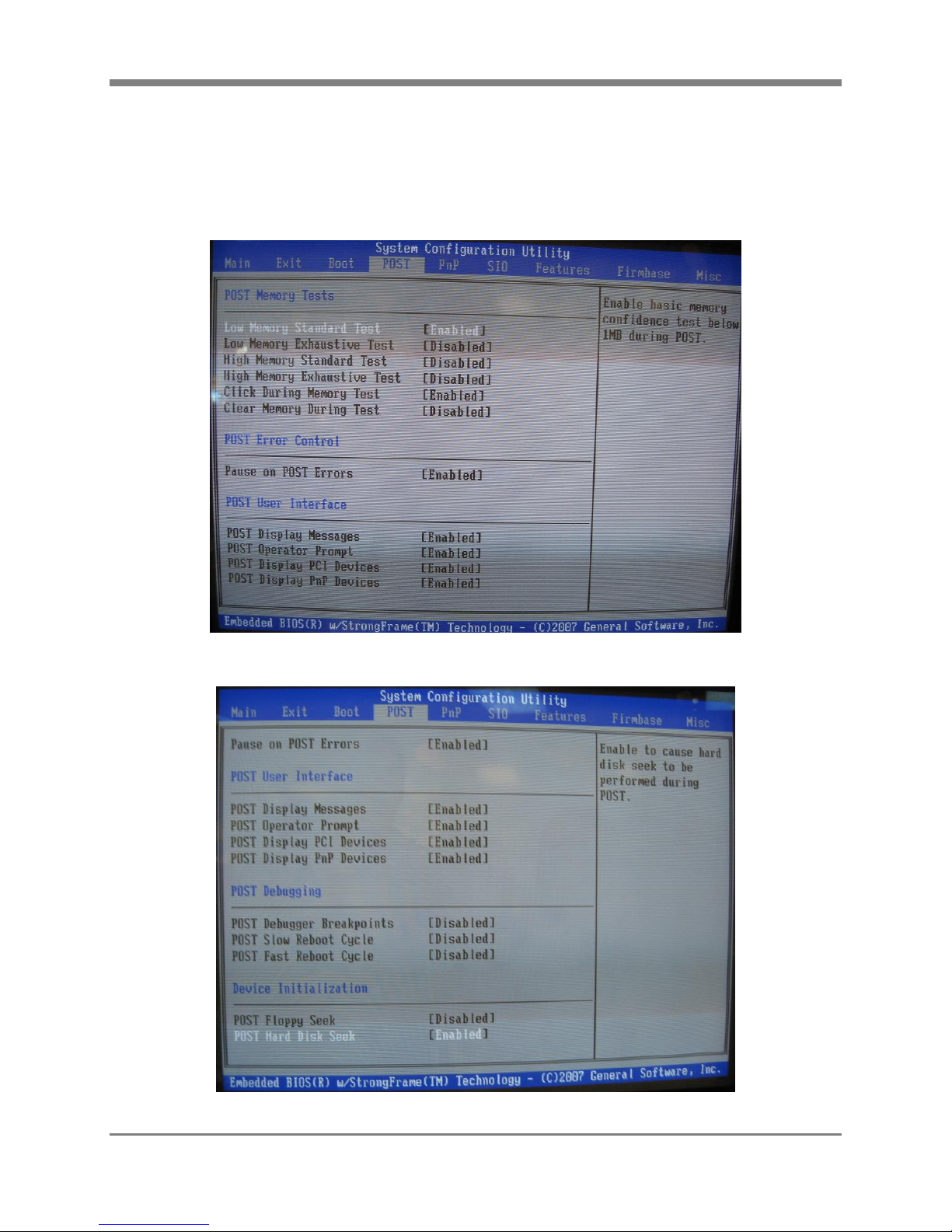
B.7 POST Setup Menu
The POST menu is used to configure POST. This menu is shown in the following figure (scrolled down more so the
full set of options can be seen.) Be sure to review the Features menu, where additional items can be configured,
such as the Splash Screen and BIOS initiatives.
The figure below shows the same menu, scrolled down so that the remainder of its fields may be
viewed.
CPU-71-10 (XPD/RPD/DPD) VMEbus Core 2 Duo Processor Board – User’s Manual 37
Page 42

Appendix B – BIOS & Setup
The following table describes the settings associated with the POST setup menu’s Memory Test section.
Low Memory Standard
Test
Low Memory Exhaustive
Test
High Memory Standard
Test
High Memory Exhaustive
Test
Huge Memory Standard
Test
Huge Memory Exhaustive
Test
Click During Memory Test Enable/disable speaker click when testing each block.
Clear Memory During Test Enable storing 0’s in all memory locations tested. Only necessary when some legacy
The following table describes the settings associated with the POST setup menu’s Error Control section:
Pause on POST Errors Enable pause when errors are detected during POST, so that the user can view the
The following table describes the settings associated with the POST setup menu’s POST User Interface section:
POST Display Messages Enable display of text messages during POST. When disabled, POST is “quiet.”
POST Operator Prompt Enable operator prompts if POST is configured to ask interactive questions of the
POST Display PCI Devices Enable display of PCI devices.
POST Display PnP Devices Enable display of ISA PnP devices.
The following table describes the settings associated with the POST setup menu’s Debugging section:
POST Debugger
Breakpoints
POST Fast Reboot Cycle Enable early reboot in POST, allowing service technician to verify that the hardware
POST Slow Reboot Cycle Enable late reboot in POST, allowing service technician to cause the system to move
The following table describes the settings associated with the POST setup menu’s Device In itialization section:
POST Floppy Seek Enable head seek on each floppy drive configured in the system. Used to recalibrate
POST Hard Disk Seek Enable head seek on each hard drive configured in the system. This is a way of
Enable basic memory confidence test, of memory below 1MB address boundary
(conventional memory, or memory normally used by DOS.)
Enable exhaustive memory confidence test of memory below 1MB address boundary.
Enable basic memory confidence test, of memory between 1MB and 4.2GB address
boundaries (extended memory.)
Enable exhaustive memory confidence test, of memory between 1MB and 4.2GB
address boundaries.
Enable basic memory confidence test, of memory above 4.2GB address boundary
(available using PAE technology.)
Enable exhaustive memory confidence test, of memory above 4.2GB address
boundary.
DOS programs are run, as they may rely on cleared memory to operate properly.
error message and enter Setup or continue to boot the OS.
user about whether to load specific features; i.e., whether or not to load SMM.
Enable processing of INT 3 (breakpoint) instructions embedded into option ROMs.
When enabled, if an INT 3 instruction is encountered, control is transferred to the
BIOS debugger, so that the option ROM can be debugged. When disabled, these
instructions perform no action.
can technician to verify that the hardware can reboot very quickly many times in
succession. Platform will continue to reboot after every boot until the system’s
CMOS is reset, as there is no way to enter Setup from this early point during POST.
through POST and then reboot, causing POST to be reexecuted, over and over, until
Setup is reentered and this option is disabled. When left unattended, this is a
straightforward way of having POST exercise system memory and peripherals
without requiring a boot to a drive with an operating system installed.
the drive in some systems with older DOS operating systems.
extending the standard testing performed on each drive during POST, by requesting
that the drive actually move the head. Not available with all drives.
38 CPU-71-10 (XPD/RPD/DPD) VMEbus Core 2 Duo Processor Board – User’s Manual
Page 43
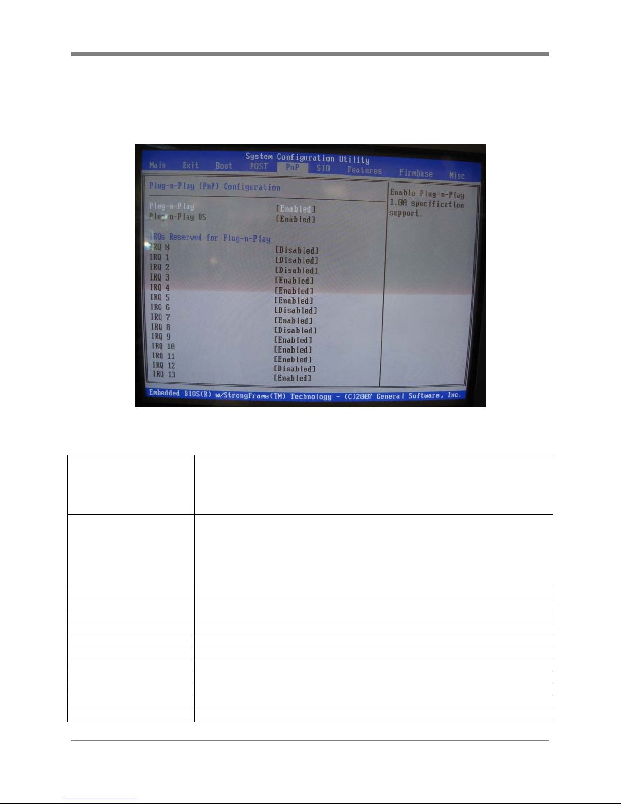
Appendix B – BIOS & Setup
B.8 PnP Setup Menu
The PnP menu is used to configure Plug-n-Play, a legacy BIOS initiative used to support operating systems such as
Windows95, Windows98, and WindowsNT. ACPI has largely replaced this feature; however, it is necessary for
platforms to support older operating systems.
The PnP menu consists of two sections; basic configuration that enables Plug-n-Play and identifies if a PnP should
perform configuration or let the OS do it; and then, another section that defines which system IRQs should be
reserved for PnP’s use, so that PCI doesn’t use them. The following table presents the fields in the PnP menu.
Plug-n-Play Enable PnP feature. When disabled, a PnPaware OS will not find any PnP services in
the BIOS, and all other configuration parameters in the menu will be greyed out.
Enable to support legacy OSes like DOS, Windows95, Windows98, and
WindowsNT. Disable for operating systems like WindowsXP or Windows Vista, or
for Linux operating systems with ACPI support.
Plug-n-Play OS Enable delay of configuration of PnP hardware and option ROMs. When enabled,
BIOS will NOT configure the devices, and instead defer assignment of resources,
such as DMA, I/O, memory, and IRQs, to the PnP OS. When disabled, the BIOS
performs conflict detection and resolution, and assigns resources for the OS. Disable
this parameter when running non-PnP OSes like DOS. Enable this parameter when
running PnP OSes like Windows95, Windows98, and WindowsNT.
IRQ0 Enable exclusive use of IRQ0 by PnP.
IRQ1 Enable exclusive use of IRQ1 by PnP.
IRQ2 Enable exclusive use of IRQ2 by PnP.
IRQ3 Enable exclusive use of IRQ3 by PnP.
IRQ4 Enable exclusive use of IRQ4 by PnP.
IRQ5 Enable exclusive use of IRQ5 by PnP.
IRQ6 Enable exclusive use of IRQ6 by PnP.
IRQ7 Enable exclusive use of IRQ7 by PnP.
IRQ8 Enable exclusive use of IRQ8 by PnP.
IRQ9 Enable exclusive use of IRQ9 by PnP.
IRQ10 Enable exclusive use of IRQ10 by PnP.
CPU-71-10 (XPD/RPD/DPD) VMEbus Core 2 Duo Processor Board – User’s Manual 39
Page 44
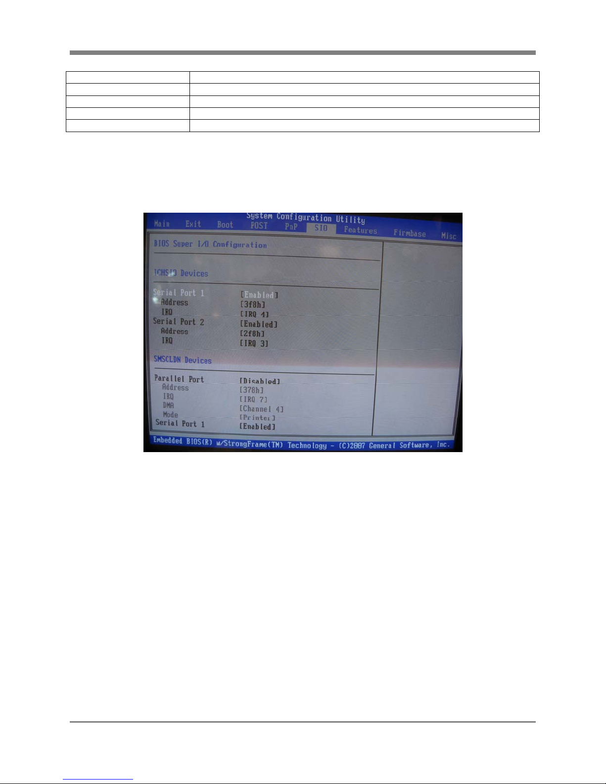
Appendix B – BIOS & Setup
IRQ11 Enable exclusive use of IRQ11 by PnP.
IRQ12 Enable exclusive use of IRQ12 by PnP.
IRQ13 Enable exclusive use of IRQ13 by PnP.
IRQ14 Enable exclusive use of IRQ14 by PnP.
IRQ15 Enable exclusive use of IRQ15 by PnP.
B.9 Super I/O (SIO) Setup Menu
The SIO menu is used to configure the LPC47B27x Super I/O device. The only implemented I/O on this chip are
the PS/2 mouse and keyboard and two 2-wire COM ports (COM3 & COM4). Basically this window is used to
configure COM3 & COM4 (though they are referred to as Serial Ports 1 & 2 in the SIO Setup Menu):
POST reads these settings in the menu shown above and programs the Super I/O part accordingly, enabling and
disabling devices as requested. The disabled devices are not further programmed, since they are actually disabled in
hardware. In the figure above, legacy I/O addresses and IRQs are as follows:
COM3 – I/O 3f8h, IRQ4.
COM4 – I/O 2f8h, IRQ3.
It should be noted that these are not the only possible addresses, but they are the ones that will ensure compatibility
with the most legacy software, especially early DOS programs that do not use BIOS to access the COM ports.
40 CPU-71-10 (XPD/RPD/DPD) VMEbus Core 2 Duo Processor Board – User’s Manual
Page 45
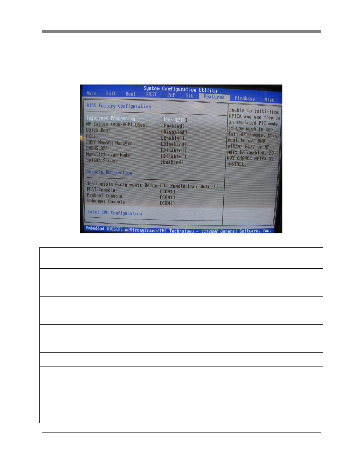
Appendix B – BIOS & Setup
B.10 Features Setup Menu
The Features menu is used to configure the system BIOS’ major features, including Quick Boot, APM, ACPI,
PMM, SMBUS, SMBIOS, Manufacturing Mode, Splash Screen, Console Redirection, and others added by the
OEM. This figure shows a typical Features Setup menu.
The following table describes each setting in the Features menu :
Quick Boot Enable time-optimized POST, causing certain preconfigured OEM optimizations to
be made when the system boots. Depending on the system, Quick Boot can reach the
DOS prompt in as little as 85ms (milliseconds.)
Advanced Power
Management (APM)
Enable legacy power management, used by the system when an ACPI-aware
operating system is not running (during POST, such as when the system is running
the preboot environment, or while running DOS, Windows95, Windows98, or Linux
kernels below version 2.6.) Uses the SMM feature (see Firmbase) to operate properly.
ACPI Enable ACPI system description and power management (ACPI replaces PnP and
APM.) Used with ACPI-aware OSes such as Linux kernels version 2.6 and above,
Windows XP, and Windows Vista. Commonly also uses the SMM feature (see
Firmbase) to operate properly.
POST Memory Manager
(PMM)
Enable memory allocation services for option ROMs, especially network cards
running PXE. Some option ROMs may use this interface incorrectly, causing system
crashes. Other PXE option ROMs may not run if PXE is not supported. Because of
the state of these option ROMs, the setting is provided as an option to the user.
SMBUS API Enable INT 15h services that permit certain software to access devices on the
system’s SMBUS without having knowledge of the SMBUS controller itself.
System Management BIOS
(SMBIOS)
Enable System Management BIOS interface specification support, exposing
information about the type of hardware, including the chassis, motherboard layout,
type of CPU and DRAM sticks, to applications such as WfM, which runs on PXE in
the preboot environment.
Manufacturing Mode Enable automatic entry into manufacturing mode when POST encounters a critical
error. Used in closed device settings such as smart phones that need access to docking
stations when they don’t boot. Leave disabled.
Splash Screen Enable graphical POST
CPU-71-10 (XPD/RPD/DPD) VMEbus Core 2 Duo Processor Board – User’s Manual 41
Page 46
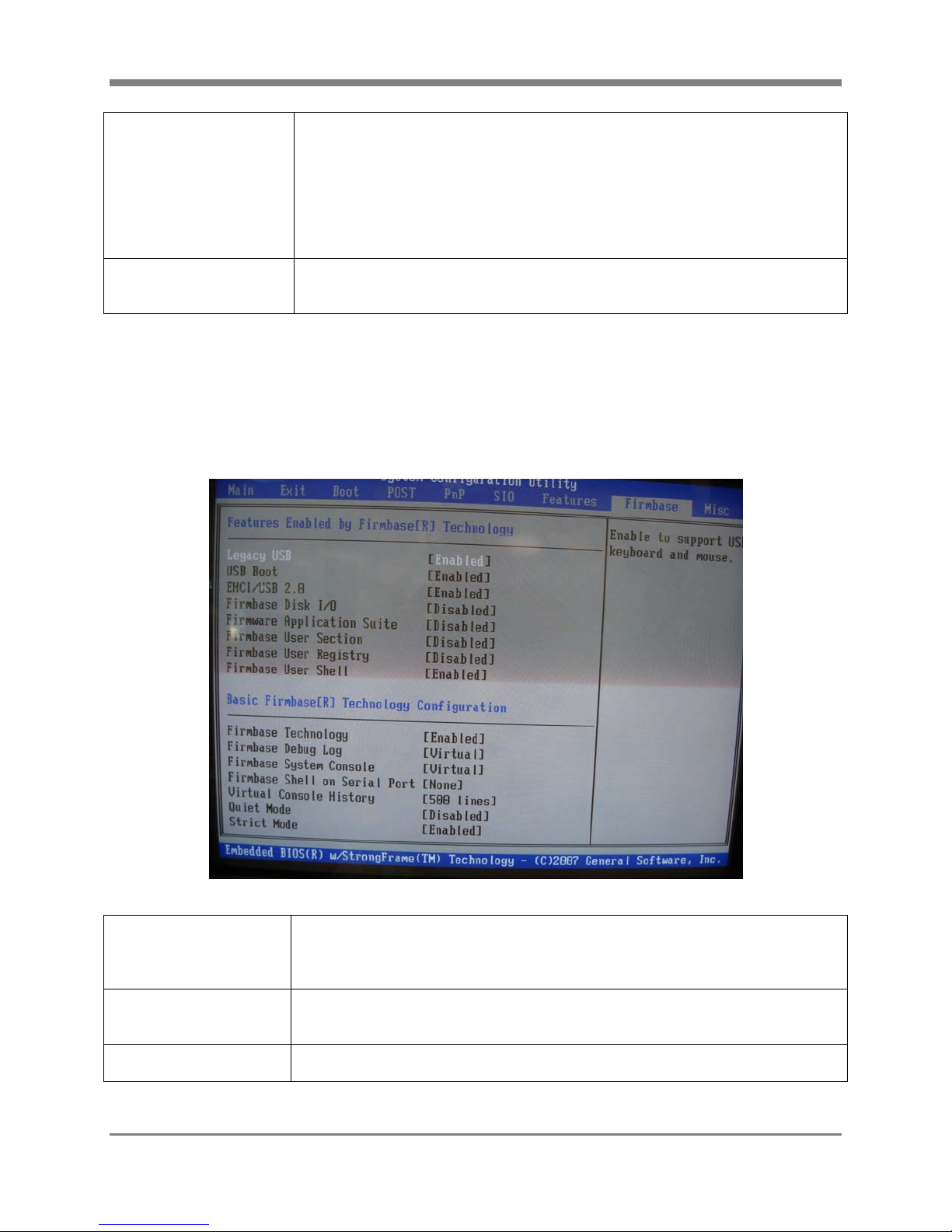
Appendix B – BIOS & Setup
Console Redirection Configure the console redirection feature over a serial port. Automatic – causes
POST, the debugger, and the preboot environment to use the system’s first serial port
(COM1) when an RS232 cable is detected with DSR and CTS modem signals active,
indicating a terminal emulation program is likely to be attached to the other end of the
cable. Always – causes the BIOS to always use the serial port as the console, without
testing for the presence of the terminal emulation program. Never – causes the BIOS
to never invoke console redirection, but instead always use the main keyboard and
video display. If there is no keyboard or video display, the system operates headless.
EFI Source Configure the location (ROM or disk) where the EFI boot action can find the
EFILDR.BIN image. An image may be merged with the system BIOS into the system
ROM, or it may be placed in the root directory of any bootable mass storage device.
B.11 Firmbase Setup Menu
The Firmbase menu configures the Firmbase Technology component of the system BIOS, including all of the
features enabled by it; i.e., legacy USB keyboard and mouse, boot from USB devices, and support of Firmbase
applications such as Boot Security, Platform Update Facility, and High Availability Monitor. This menu has several
parts, with the most basic user oriented feature options in the top section, and the more technical tuning parameters
located in the lower sections.
The following table presents the settings that enable high-level features enabled by Firmbase Technology:
Legacy USB Enables BIOS support for USB keyboards and mice. Up to 8 USB keyboards and 8
USB mice may be supported at a time. Use of PS/2 keyboard and mouse concurrently
with USB devices is discouraged, as the legacy PS/2 keyboard controller cannot
easily separate simultaneous data streams from both device classes.
USB Boot Enables BIOS support for accessing USB mass storage devices and emulating legacy
floppy, hard drive, and CDROM drive devices with them. Enable this option in order
for USB devices to be supported in the BBS device list(see the BOOT menu.)
EHCI/USB 2.0 Enables EHCI Firmbase Technology driver, allowing USB Boot feature to use high
speed transfers on USB 2.0 ports in the system.
42 CPU-71-10 (XPD/RPD/DPD) VMEbus Core 2 Duo Processor Board – User’s Manual
Page 47

Appendix B – BIOS & Setup
Firmbase Disk I/O Enables Firmbase Technology FAT file system driver, so that Firmbase applications
such as Boot Security, Platform Update Facility, and HA Monitor, as well as the HA
and TCB components of the kerne, have access to files residing on drives containing
FAT file systems. Also turn on this option if you wish to run Firmbase applications
from FAT file systems on either ATA or USB mass storage devices.
Firmware Application
Suite
Firmbase User Registry Not used.
Firmbase User Shell Enables Firmbase Technology command line interpreter, a multi-user command shell
Firmbase Technology Enables Firmbase Technology as a whole, the industry’s most comprehensive and
Firmbase Debug Log Specifies the device used by Firmbase Technology components (kernel, drivers, and
Firmbase System Console Specifies the device used by Firmbase Technology’s system process when it
Firmbase Shell on Serial
Port
Enables Firmbase applications configured for the system by the OEM. Typically
includes Boot Security, Platform Update Facility, and High Availability Monitor.
with DOS-like and Unix-like command structure;can be used to start Firmbase
applications written with the Firmbase SDK, a General Software product.
fullfeatured System Management Mode (SMM) operating environment. Some
hardware platforms require Firmbase Technology to run, as they may use it to
virtualize hardware such as virtual video and audio PCI devices. Some BIOS features,
such as ACPI and APM, may require Firmbase Technology to operate
programs) to display debugging instrumentation produced with the dprintf and
DPRINTF system functions.
None – Instrumentation disabled.
COM1 – Write text to 1st serial port.
COM2 – Write text to 2nd serial port.
COM3 – Write text to 3rd serial port.
COM4 – Write text to 4th serial port.
Virtual – Write text to virtual console
If enabled, this console can provide diagnostic messages (similar to the types
displayed by Linux when it boots) for Firmbase Technology features such as USB
HID and USB Boot.
initializes the kernel and processes the [SYSTEM] registry section, including its Start
and Run commands.
None – System console disabled.
COM1 – Write text to 1st serial port.
COM2 – Write text to 2nd serial port.
COM3 – Write text to 3rd serial port.
COM4 – Write text to 4th serial port.
Virtual – Write text to virtual console
If enabled, this console can provide a list of sign-on banners of all Firmbase
applications loaded during system initialization.
Specifies a serial port that may be used by Firmbase Technology’s command line
interpreter as an extra user session for systems that do not have a keyboard or monitor
to support virtual consoles.
None – Serial console disabled.
COM1 – Console on 1st serial port.
COM2 – Console on 2nd serial port.
COM3 – Console on 3rd serial port.
COM4 – Console on 4th serial port.
CPU-71-10 (XPD/RPD/DPD) VMEbus Core 2 Duo Processor Board – User’s Manual 43
Page 48
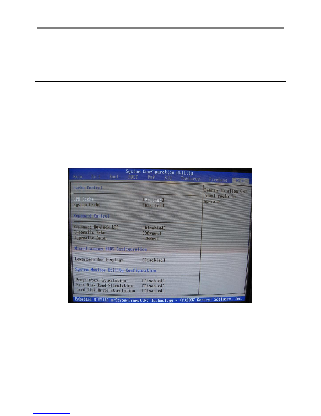
Appendix B – BIOS & Setup
Virtual Console History Specifies the number of lines of text that Firmbase Technology maintains in its virtual
console feature, allowing the user to scrollback through lines previously displayed
and
scrolled off the screen. OEMs may configure a set of values, such as 20, 50, 100, 200,
and 500 lines.
Quiet Mode Enables a feature that causes the Firmbase kernel to suppress its standard messages to
the system console.
Strict Mode Enables a feature that causes the Firmbase kernel to abort any processes in the system
that make software errors in calling system API functions. Examples include blocking
at IRQLs other than IRQL_THREAD, or passing a NULL pointer to a C library
function that requires a non-NULL pointer, etc.
Disabling this feature causes the kernel to skip over the activity th at discovered the
programming error in the application, allowing it to continue if at all possible, with
the consequence that the program may not operate correctly.
B.12 Miscellaneous Setup Menu
The Misc menu provides for configuration of BIOS settings that don’t easily fit in any other category. They include
Cache Control, Keyboard Control, Debugger Settings, and System Monitor Utility Configuration parameters.
The following table presents the settings in the Misc Setup menu:
System Cache Enables POST’s support for cache in the system. Modern processors virtually require
cache to be enabled to achieve acceptable performance. However, to diagnose certain
problems related to caching in the system, such as multiprocessing systems, it may be
desirable to disable this setting.
Keyboard Numlock LED Enables the Numlock key when POST initializes the PS/2 keyboard.
Typematic Rate Specify the rate at which the PS/2 keyboard controller repeats characters when most
keys are pressed down. USB typematic is automatic and does not use this parameter.
Typematic Delay Specifies the amount of time a repeating key may be pressed on a PS/2 keyboard until
the key repeat feature begins repeating the keystroke. USB typematic is automatic and
does not use this parameter.
44 CPU-71-10 (XPD/RPD/DPD) VMEbus Core 2 Duo Processor Board – User’s Manual
Page 49

Appendix B – BIOS & Setup
Lowercase Hex Displays Enables the display of hexadecimal numbers in the debugger with lowercase letters
instead of uppercase letters (ie, 2f8ah instead of 2F8AH.)
Proprietary Stimulation Enables System Monitor’s callout to the OEM’s BPM adaptation code to execute code
that causes stimulation of the SMM environment for measurement purposes.
Hard Disk Read
Stimulation
Hard Disk Write
Stimulation
Floppy Disk Read
Stimulation
Enables System Monitor’s read of a preconfigured number of sectors from a location
on the first hard disk in the system in order to stimulate the SMM environment. This is
useful when measuring code path lengths in USB boot, when the first hard drive is
configured in the BBS list as a USB hard drive.
Enables System Monitor’s write of a preconfigured number of sectors to a location on
the first hard disk in the system in order to stimulate the SMM environment. This is
useful when measuring code path lengths in USB boot, when the first hard drive is
configured in the BBS list as a USB hard drive.
Please note that when this parameter is selected, the system automatically enables
reading, so that the stimulation of the system includes reading a range of sectors into a
memory buffer, and writing the same data back to the same range of sectors for safety.
Thus, this feature is theoretically nondestructive.
WARNING: YOU ARE ADVISED THAT THIS FEATURE COULD CAUSE
DATA LOSS AT YOUR SOLE EXPENSE; ACCORDINGLY, IT IS PROVIDED
AS-IS WITHOUT WARRANTY OF ANY KIND. ALWAYS BACKUP YOUR
DATA BEFORE PERFORMING DIAGNOSTICS ON ANY SYSTEM, AS THEY
COULD CAUSE DATA LOSS.
There is no Floppy Drive interface implemented on the DPD.
CPU-71-10 (XPD/RPD/DPD) VMEbus Core 2 Duo Processor Board – User’s Manual 45
Page 50

Appendix B – BIOS & Setup
46 CPU-71-10 (XPD/RPD/DPD) VMEbus Core 2 Duo Processor Board – User’s Manual
Page 51
Appendix C – Power & Environment Requirements
C. Power and Environmental Requirements
The XPD power and environmental requirements are shown in the tables below.
Condition Power Requirements
1.66 GHz Core Duo +5 VDC @ 6.0 A typ.
3.0 VDC Lithium Coin Cell @ 3.4 A
Power Requirements
The 3 Volt lithium coin cell is a CR2032 with 190 mAhours capacity and it is used to battery-back the Real Time
Clock, the 2 MB of NV-SRAM, and the BIOS’s NV-RAM. At 3.4 A this battery should last for over six years
with power off.
Condition Environmental Requirements
Operating Temperature
Storage Temperature
-20 to 85 C with Thermal Monitor II
enabled
-50 to +105 C
Environmental Requirements
CPU-71-10 (XPD/RPD/DPD) VMEbus Core 2 Duo Processor Board – User’s Manual 47
Page 52

Appendix C – Power & Environment Requirements
48 CPU-71-10 (XPD/RPD/DPD) VMEbus Core 2 Duo Processor Board – User’s Manual
Page 53
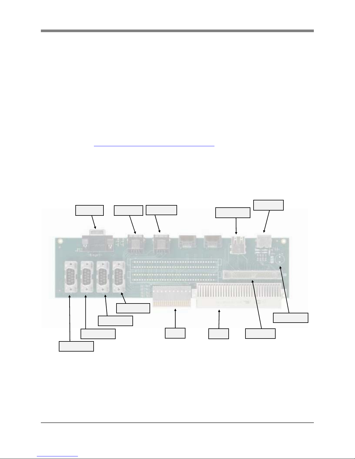
Appendix D – XPDPTB Rear Plug-in I/O Expansion Module for the XPD
D. XPDPTB Rear Plug-in I/O Expansion Module for the XPD
Dynatem offers a rear plug-in paddle card for I/O expansion with the XPD. Essentially the XPDPTB routes the
XPD’s backplane I/O, including IDE, COM1/2/3/4, P/S2 Mouse/Keyboard interfaces, VGA, two USB ports, and
two SATA ports to industry standard connectors.
IDE, the four COM ports, two USB ports, and mouse and keyboard ports are routed through P2. The two Ethernet
ports, two SATA ports, and the VGA port are routed through P0.
Two Serial ATA ports are routed through RP0. The XPDPTB also routes two VITA 31.1 compliant 1 Gb Ethernet
ports from RP0 to two industry standard connectors for situations where VITA 31.1 backplane fabric switching is
not used.
The Super I/O device used for COM3/4, P/S2 Mouse/Keyboard, LPT1, and FDC is SMSC’s LPC47B272 and a data
sheet can be found at: http://www.smsc.com/main/catalog/lpc47b27x.html
Here is a photograph of the XPDPTB with the connectors indicated:
VGA – J11
LANA – J7
LANB – J6
USB2&3 – J8
PS2 – J12
SATA0 SATA1
COM4 – J1
COM3 – J2
Reset Button
COM2 – J4
COM1 – J3
RP0
RP2
IDE – J5
CPU-71-10 (XPD/RPD/DPD) VMEbus Core 2 Duo Processor Board – User’s Manual 49
Page 54
Appendix D – XPDPTB Rear Plug-in I/O Expansion Module for the XPD
D.1 XPDPTB Connector Pinouts
Pin Signal Pin Signal
1 RST# 2 GND
3 D7 4 D8
5 D6 6 D9
7 D5 8 D10
9 D4 10 D11
11 D3 12 D12
13 D2 14 D13
15 D1 16 D14
17 D0 18 D15
19 GND 20 No connection
21 DMARQ0 22 GND
23 IOW# 24 GND
25 IOR# 26 GND
27 IORDY 28 470-ohm pull-down
29 DMAACK0 30 GND
31 IRQ14 32 No connection
33 DA1 34 No connection
35 DA0 36 DA2
37 CS1Fx 38 CS3Fx
39 LED Control 40 GND
Primary IDE Interface Connector (J5) – 40-pin Dual-row 0.1” Header
COM1 and COM2 ports are set up for RS-232 operation. J3 is used for COM1 and J4 is used for COM2. The
pinouts of the two connectors are identical:
Pin RS-232 Signals
1 Data Carrier Detect (DCD) Input
2 Received Data (RxD) Input
3 Transmitted Data (TxD) Output
4 Data Terminal Ready (DTR) Output
5 GND
6 Data Set Ready (DSR) Input
7 Request To Send (RTS) Output
8 Clear To Send (CTS) Input
9 Ring Indicator (RI) Input
COM1 (J3) and COM2 (J4) Connectors – DB9M Connector. The metal shell of the connector goes
to chassis ground.
50 CPU-71-10 (XPD/RPD/DPD) VMEbus Core 2 Duo Processor Board – User’s Manual
Page 55
Appendix D – XPDPTB Rear Plug-in I/O Expansion Module for the XPD
COM3 and COM4 ports are set up for two-wire RS-232 operation. J2 is used for COM3 and J1 is used for COM4.
The pinouts of the two connectors are identical:
Pin RS-232 Signals
1 No Connect
2 Received Data (RxD) Input
3 Transmitted Data (TxD) Output
4 No Connection
5 GND
6 No Connect
7 No Connect
8 No Connect
9 No Connect
COM3 (J2) and COM4 (J1) Connectors – DB9M Connector. The metal shell of the connector goes
to chassis ground.
J9 (SATA1) and J10 (SATA0) are Serial ATA connectors where both ports have the following pinout:
Pin Signal
1 GND
2 A+
3 A4 GND
5 B6 B+
7 GND
Serial ATA Connectors (J9, J10) - Pinout for either of the connectors
J12 combines the PS/2 Mouse and Keyboard interfaces on one connector. A Y-splitter cable is required to separate
them.
Pin Signal Description
1 Keyboard Data
2 Mouse Data
3 GND
4 +5 VDC (via 1 amp self-resetting fuse F1)
5 Keyboard Clock
6 Mouse Clock
Keyboard/Mouse Connector (J12) –Mini-DIN Receptacle. The metal shell of the connector goes to
chassis ground.
CPU-71-10 (XPD/RPD/DPD) VMEbus Core 2 Duo Processor Board – User’s Manual 51
Page 56

Appendix D – XPDPTB Rear Plug-in I/O Expansion Module for the XPD
The XPDPTB uses two RJ45 connectors to provide two 1 Gb Ethernet ports. These lines are routed through 0 ohm
resistors R1 – R16. These ports are also routed to the P0 connector in compliance with VITA 31.1. Leave the
resistors off in systems that utilize Vita 31.1 backplane networking.
J7
Pin 10/100 Signal Description Gb Signal Description
A1 Port A Transmit Data + (TX+) TP0+
A2 A Transmit Data - (TX-) TP0A3 A Receive Data + (RX+) TP1+
A4 Unused TP2+
A5 Unused TP2A6 A Receive Data - (RX-) TP1A7 Unused TP3+
A8 Unused TP3-
J6
Pin 10/100 Signal Description Gb Signal Description
B1 Port B Transmit Data + (TX+) TP0+
B2 B Transmit Data - (TX-) TP0B3 B Receive Data + (RX+) TP1+
B4 Unused TP2+
B5 Unused TP2B6 B Receive Data - (RX-) TP1B7 Unused TP3+
B8 Unused TP3-
10BaseT/100BaseTX Fast Ethernet Connector (J7/J6) – RJ45 Connectors. The metal shell of the
connectors go to chassis ground.
J8 is a dual-USB connector. Each connector has the same pinout as shown in Section A.3.
52 CPU-71-10 (XPD/RPD/DPD) VMEbus Core 2 Duo Processor Board – User’s Manual
Page 57
Appendix D – XPDPTB Rear Plug-in I/O Expansion Module for the XPD
DYNATEM
Toll free: +1 800.543.3830
Tel: +1 949.855.3235
Fax: +1 949.770.3481
Email: [email protected]
Email: [email protected]
Web: www.dynatem.com
CPU-71-10 (XPD/RPD/DPD) VMEbus Core 2 Duo Processor Board – User’s Manual 53
 Loading...