

Page 1
Embedded Solutions Page 1
DYNAMIC ENGINEERING
150 DuBois St. Suite 3, Santa Cruz, Ca 95060
831-457-8891 Fax 831-457-4793
http://www.dyneng.com
sales@dyneng.com
Est. 1988
User Manual
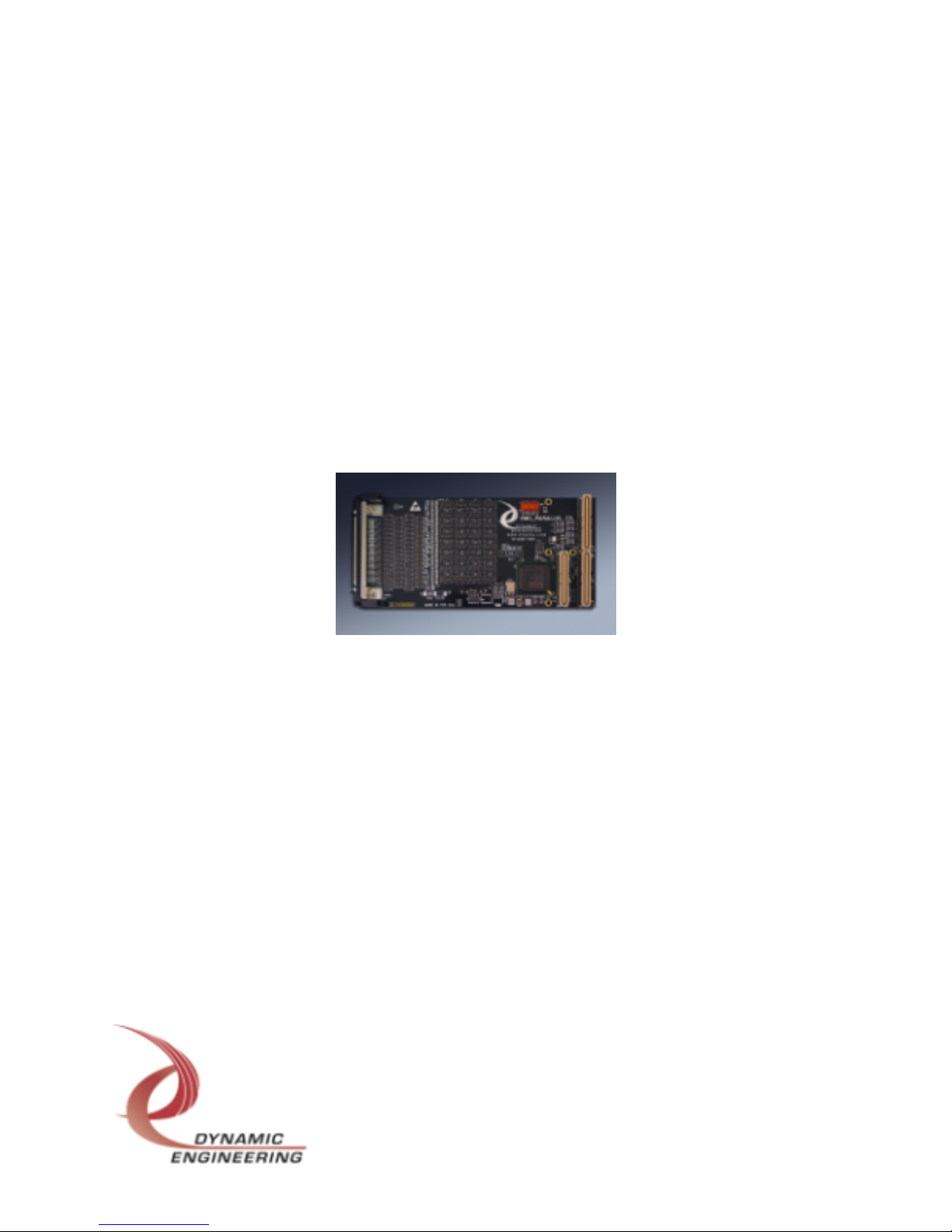
PMC-PARALLEL-TTL
Digital Parallel Interface
PMC Module
Revision A1
Corresponding Hardware: Revision 1
10-2007-0101
FLASH 0101
Page 2

Embedded Solutions Page 2
PMC-PARALLEL-TTL
Digital Parallel Interface
PMC Module
Dynamic Engineering
150 DuBois St. Suite 3, Santa Cruz CA 95060
831-457-8891 831-457-4793 FAX
This document contains information of proprietary interest to Dynamic Engineering. It
has been supplied in confidence and the recipient, by accepting this material, agrees
that the subject matter will not be copied or reproduced, in whole or in part, nor its
contents revealed in any manner or to any person except to meet the purpose for which
it was delivered.
Dynamic Engineering has made every effort to ensure that this manual is accurate and
complete. Still, the company reserves the right to make improvements or changes in the
product described in this document at any time and without notice. Furthermore,
Dynamic Engineering assumes no liability arising out of the application or use of the
device described herein.
The electronic equipment described herein generates, uses,
and can radiate radio frequency energy. Operation of this equipment in a residential
area is likely to cause radio interference, in which case the user, at his own expense,
will be required to take whatever measures may be required to correct the interference.
Dynamic Engineering’s products are not authorized for use as critical components in life
support devices or systems without the express written approval of the president of
Dynamic Engineering.
This product has been designed to operate with PMC Module carriers and compatible
user-provided equipment. Connection of incompatible hardware is likely to cause
serious damage.
©2007 by Dynamic Engineering.
Other trademarks and registered trademarks are owned by their respective manufacturers.
Manual Revision A1. Revised 9/4/07
Page 3

Embedded Solutions Page 3
Table of Contents
PRODUCT DESCRIPTION 6
THEORY OF OPERATION 9
ADDRESS MAP 11
PROGRAMMING 12
Register Definitions 13
pmcparttl_BASE 13
pmcparttl_ID 14
pmcparttl_STATUS 15
pmcparttl_DirL 16
pmcparttl_DirU 16
pmcparttl_DatL 17
pmcparttl_DatU 17
pmcparttl_DatLreg 18
pmcparttl_DatUreg 18
pmcparttl_COSclk 19
pmcparttl_RisLreg 20
pmcparttl_RisUreg 20
pmcparttl_FallLreg 21
pmcparttl_FallUreg 21
pmcparttl_IntRisLreg 22
pmcparttl_IntRisUreg 22
pmcparttl_IntFallLreg 23
pmcparttl_IntFallUreg 23
pmcparttl_IntRisLstat 24
pmcparttl_IntRisUstat 24
pmcparttl_IntRisLstat 25
pmcparttl_IntRisUstat 25
PMC MODULE LOGIC INTERFACE PIN ASSIGNMENT 26
PMC MODULE LOGIC INTERFACE PIN ASSIGNMENT 27
PMC MODULE FRONT PANEL IO INTERFACE PIN ASSIGNMENT 28
PMC MODULE BACKPLANE IO INTERFACE PIN ASSIGNMENT 29
Page 4

Embedded Solutions Page 4
APPLICATIONS GUIDE 30
Interfacing 30
Construction and Reliability 31
Thermal Considerations 32
Service Policy 33
Out of Warranty Repairs 33
SPECIFICATIONS 34
ORDER INFORMATION 35
Page 5

Embedded Solutions Page 5
List of Figures
FIGURE 1 PMC-PARALLEL-TTL REAR VIEW 7
FIGURE 2 PMC-PARALLEL-TTL BLOCK DIAGRAM 10
FIGURE 3 PMC-PARALLEL-TTL INTERNAL ADDRESS MAP 11
FIGURE 4 PMC-PARALLEL-TTL CONTROL PORT 0 BIT MAP 13
FIGURE 5 PMC-PARALLEL-TTL ID AND SWITCH BIT MAP 14
FIGURE 6 PMC-PARALLEL-TTL STATUS PORT BIT MAP 15
FIGURE 7 PMC-PARALLEL-TTL DIRECTION LOWER BIT MAP 16
FIGURE 8 PMC-PARALLEL-TTL DIRECTION UPPER BIT MAP 16
FIGURE 9 PMC-PARALLEL-TTL DATA IO LOWER BIT MAP 17
FIGURE 10 PMC-PARALLEL-TTL DATA IO UPPER BIT MAP 17
FIGURE 11 PMC-PARALLEL-TTL DATA REG LOWER BIT MAP 18
FIGURE 12 PMC-PARALLEL-TTL DATA REG UPPER BIT MAP 18
FIGURE 13 PMC-PARALLEL-TTL COS CLK CONTROL BIT MAP 19
FIGURE 14 PMC-PARALLEL-TTL RISING LOWER BIT MAP 20
FIGURE 15 PMC-PARALLEL-TTL RISING UPPER BIT MAP 20
FIGURE 16 PMC-PARALLEL-TTL FALLING LOWER BIT MAP 21
FIGURE 17 PMC-PARALLEL-TTL FALLING UPPER BIT MAP 21
FIGURE 18 PMC-PARALLEL-TTL INT RISING LOWER BIT MAP 22
FIGURE 19 PMC-PARALLEL-TTL INT RISING UPPER BIT MAP 22
FIGURE 20 PMC-PARALLEL-TTL INT FALLING LOWER BIT MAP 23
FIGURE 21 PMC-PARALLEL-TTL INT FALLING UPPER BIT MAP 23
FIGURE 22 PMC-PARALLEL-TTL RISING COS STATUS LOWER 24
FIGURE 23 PMC-PARALLEL-TTL RISING COS STATUS UPPER 24
FIGURE 24 PMC-PARALLEL-TTL FALLING COS STATUS LOWER 25
FIGURE 25 PMC-PARALLEL-TTL FALLING COS STATUS UPPER 25
FIGURE 26 PMC-PARALLEL-TTL PN1 INTERFACE 26
FIGURE 27 PMC-PARALLEL-TTL PN2 INTERFACE 27
FIGURE 28 PMC-PARALLEL-TTL FRONT PANEL INTERFACE 28
FIGURE 29 PMC-PARALLEL-TTL PN4 INTERFACE 29
Page 6

Embedded Solutions Page 6
Product Description
In embedded systems many of the interconnections are made with single ended TTL or
CMOS level signals. Depending on the system architecture an IP or a PMC will be the
right choice to make the connection. With most architectures you have a choice as
there are carriers for cPCI, PCI, VME, PC/104p and other buses for both PMC and IP
mezzanine modules.
Usually the choice is based on other system constraints as both the PMC and IP can
provide the IO you require. Dynamic Engineering would be happy to assist in your
decision regarding architecture and other trade-offs with the PMC / IP decision.
Dynamic Engineering has carriers for IP and PMC modules for most architectures, and
is adding more as new solutions are requested and required by our customers.
If you are interested in an IP module solution please refer to the IP-Parallel-IO.
PMC-Parallel-TTL is an upgrade for the PMC-Parallel-IO. After 8 years of production,
numerous updates to handle obsolete parts, and new customer requirements it is time
for an updated design. The PMC Parallel IO is still available for clients who have
designed it into their systems. The PMC Parallel TTL is recommended for new systems
and to upgrade current designs. The connector pinouts are retained for ease of system
migration.
The PMC compatible PMC-Parallel-TTL has 64 independent digital IO. The high density
makes efficient use of PMC slot resources. The IO is available for system connection
through the front panel, via the rear [Pn4] connector, or both. A high density 68 pin
SCSI III front panel connector provides the front panel IO. The IO lines can be
protected with optional transorbs. The rear panel IO has a PIM and PIM Carrier
available for rear panel wiring options.
The HDEterm68 http://www.dyneng.com/HDEterm68.html
can be used as a breakout for the front or rear panel IO. The HDEcabl68 provides a
convenient cable. http://www.dyneng.com/HDEcabl68.html Custom cables can be
manufactured to your requirements. Please contact Dynamic Engineering with your
specifications.
Each channel is programmable to be input or output on a channel-by-channel basis. All
64 IO channels can be used as interrupt generators. Interrupts are programmable to be
based on rising, falling and change of state [both] conditions. The interrupts are
maskable to allow polled operation as well.
The inputs are available unfiltered and after the transition detection. The transition
detection is programmable for clock rate. The local 50 MHz oscillator, PCI or external
clocks can be selected as the reference to the clock divider. The clock divider is
Page 7
Embedded Solutions Page 7
programmable to use the reference rate or to divide it to a lower frequency. An optional
PLL capability is available for users who require more extensive frequency options.
All of the IO are routed through the FPGA to allow for custom applications that require
hardware intervention or specific timing- for example an automatic address or data
strobe to be generated. The initial model is register based. The design is DMA
capable and can be used for more intensive applications of data capture or delivery.
Please contact Dynamic Engineering with your requirements.
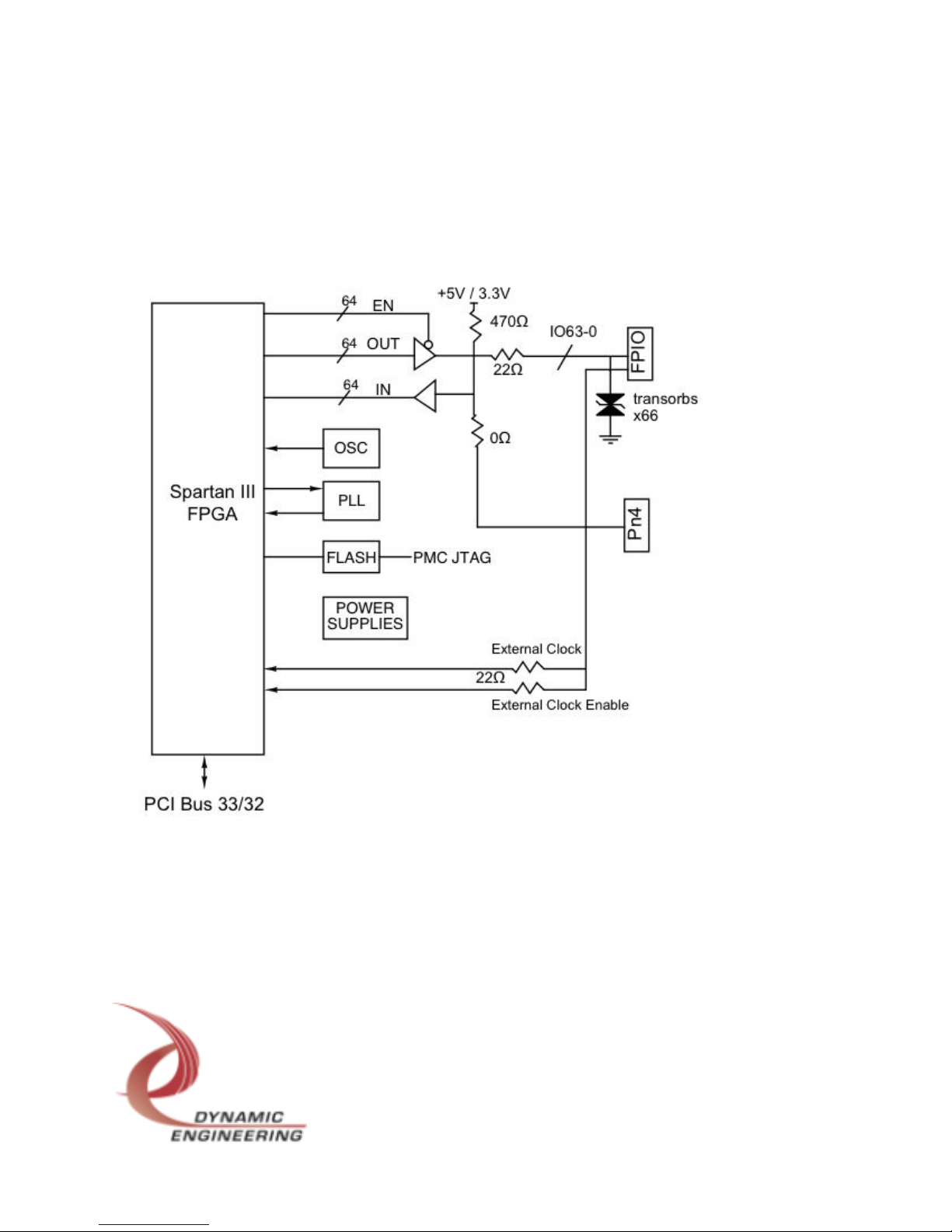
The IO are driven with open-drain high current drivers. When enabled, the high side is
driven with the device and augmented with pull-up resistors. When disabled the output
is pulled high with the resistors unless another device on the line is driving that line low.
The low side of the driver can sink 64+ mA. The high side drive is a few mA. All IO
have 2 pull-up locations per line. The default is for 470 ohms installed into one location.
The multiple locations allow for pull-up strengths greater than 470 ohms, and to stay
within the resistor pack wattage capabilities. The multiple packs also allow for parallel
combinations to create more options of specific pull-up values. For custom models with
additional pull-ups or alternate values please contact Dynamic Engineering. The two
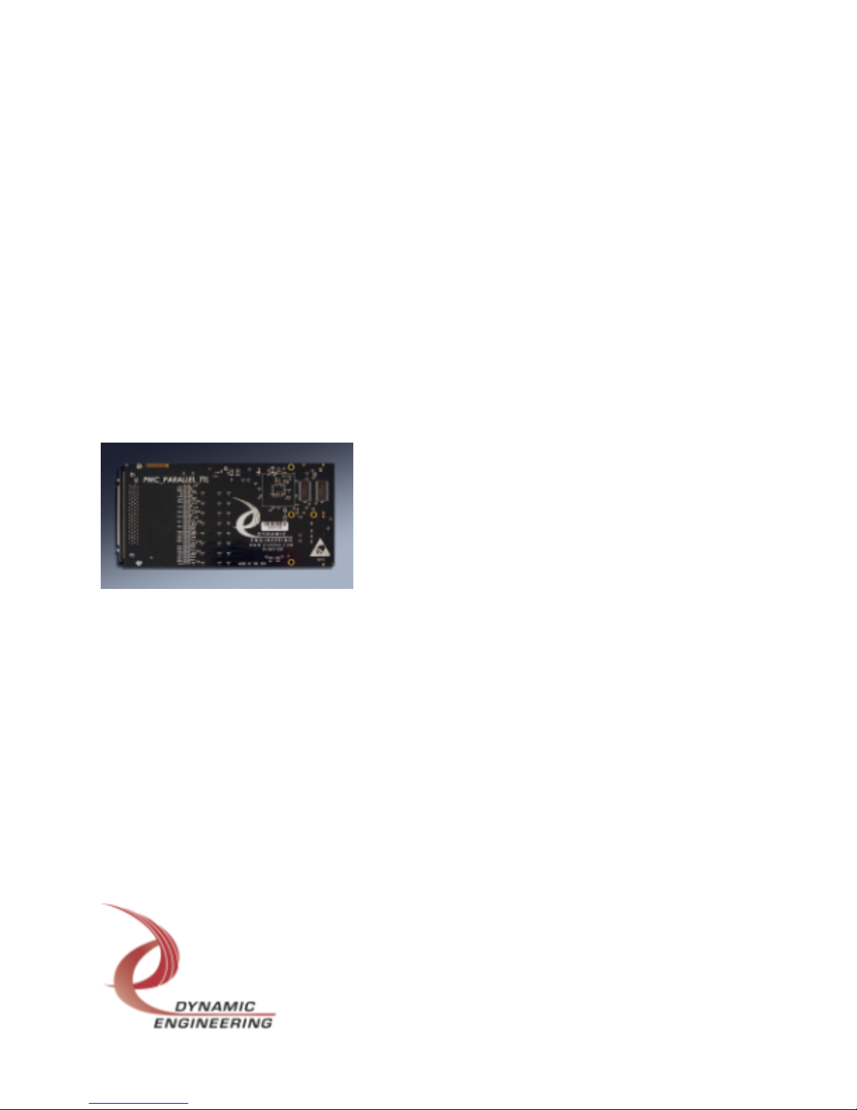
columns of pull-up resistor locations are visible on the rear of the card.
Figure 1 PMC-PARALLEL-TTL REAR VIEW
The registers are mapped as 32 bit words and support byte, word and 32 bit access. All
registers are read-writeable. The Windows® compatible [XP/2000] driver is available to
provide the system level interface for this design. Use standard C/C++ to control your
hardware or use the Hardware manual to make your own software interface. The
software manual is also available on-line.
The basic functions of parallel IO and COS capture are designed into the base model.
Additional features will be added to the base model by using a mux on the output side to
allow software to select the base or extended features. Data bit 0 is the first extended
feature and is a programmable output for the COS reference clock. With software the
output definition can be changed to drive the COS clock onto Data 0. The user can use
a scope to check that their set-up is what they want it to be and then likely return it to
being a data bit. You can leave is as a clock if desired. Additional features will be
incorporated into the base design in a manner where the default is the initial base
Page 8

Embedded Solutions Page 8
design => to prevent updates from conflicting with existing software. The FLASH on the
current boards will be able to be updated to use the new features in most cases.
PMC-PARALLEL-TTL is part of the PMC Module family of modular I/O components.
The PMC-PARALLEL-TTL conforms to the PMC standard. This guarantees
compatibility with multiple PMC Carrier boards. Because the PMC may be mounted on
different form factors, while maintaining plug and software compatibility, system
prototyping may be done on one PMC Carrier board, with final system implementation
on a different one.
Page 9

Embedded Solutions Page 9
Theory of Operation
The PMC-PARALLEL-TTL can be used for multiple purposes with applications in
telecommunications, control, sensors, IO, test; anywhere multiple independent IO are
useful.
The PMC-PARALLEL-TTL features a Xilinx FPGA, and high current LVTH driver
devices. The FPGA contains the PCI interface and control required for the parallel
interface.
The Xilinx design incorporates the “PCI Core” and additional modules for DMA in
parallel with a direct register decoded programming model. The initial implementation
provides an enhanced feature set based on the PMC Parallel IO design. Additional
FLASH updates will provide DMA, pattern generation, pulse generation, and user
defined requirements.
The drivers are initialized to the off state and pull-ups on board hold the IO lines in the
‘high’ state. The direction registers are used to program the channel to be a driver or
not. The receivers are always enabled allowing local read-back of the transmitted data.
Data written to the IO registers can be placed on the bus. The master enable allows all
64 channels to be synchronized if desired. The master enable can be programmed “on”
to allow direct updates if 64 bit synchronization is not required.
For an IO with the direction bit set and master enabled: When a ‘0’ is written to any IO
line register position the corresponding line is driven low. When a ‘1’ is written to any IO
line register position that line is un-driven by the local driver and the output level will be
controlled by the termination resistor, and any other drivers attached to that line. The
control register is read-writeable. The data register read corresponds to the IO side.
The register read-back is at an alternate address offset. The register read-back is
independent of the bus; the data read will always match the data written. The IO data
read will reflect the state of the bus and not necessarily the state of the on-board
drivers.
The read-back registers are clocked at a programmable rate with an internal clock
generator. If desired the internal clock can be replaced with an external source and an
enable. The basic option is available under SW control. If special programming is
needed please contact Dynamic Engineering for a custom FPGA implementation.
All the IO control and registers are instantiated within the FPGA, only the drivers and
receivers are separate devices. If desired, the IO lines can be specially programmed
to create custom timing pulses etc. For example if the interface is to put out an address
Page 10
Embedded Solutions Page 10
and then an address qualifier to strobe the address into the receiving hardware one of
the IO lines can be programmed to create a pulse some time after the address for the
IO registers is written to. The custom pulse will be more accurate for delay and duration
than a SW timing solution. The number of accesses to the card can be reduced as well
having the effect of greater through-put. Please contact Dynamic Engineering with your
requirements.
Figure 2 PMC-PARALLEL-TTL Block Diagram
Page 11

Embedded Solutions Page 11
Address Map
Function Offset
// PMC Parallel TTL definitions
#define pmcparttl_BASE 0x0000 // 0 PMC Parallel TTL base control register offset
#define pmcparttl_ID 0x0004 // 1 PMC Parallel TTL ID Register offset
#define pmcparttl_STATUS 0x0008 // 2 PMC Parallel TTL status Register offset
#define pmcparttl_DirL 0x000c // 3 PMC Parallel TTL Direction lower Register offset
#define pmcparttl_DirU 0x0010 // 4 PMC Parallel TTL Direction upper Register offset
#define pmcparttl_DatL 0x0014 // 5 PMC Parallel TTL Data lower Register, line data read
#define pmcparttl_DatU 0x0018 // 6 PMC Parallel TTL Data upper Register, line data read
#define pmcparttl_DatLreg 0x001c // 7 PMC Parallel TTL Data lower Register read-back
#define pmcparttl_DatUreg 0x0020 // 8 PMC Parallel TTL Data upper Register read-back
#define pmcparttl_COSclk 0x0024 // 9 PMC Parallel TTL COS Clock definition Register
//#define spare 0x0028 // 10 PMC Parallel TTL
#define pmcparttl_RisLreg 0x002c // 11 PMC Parallel TTL Rising lower Register
#define pmcparttl_RisUreg 0x0030 // 12 PMC Parallel TTL Rising upper Register
#define pmcparttl_FallLreg 0x0034 // 13 PMC Parallel TTL Falling lower Register
#define pmcparttl_FallUreg 0x0038 // 14 PMC Parallel TTL Falling upper Register
#define pmcparttl_IntRisLreg 0x003c // 15 PMC Parallel TTL Interrupt Enable Rising lower Register
#define pmcparttl_IntRisUreg 0x0040 // 16 PMC Parallel TTL Interrupt Enable Rising upper Register
#define pmcparttl_IntFallLreg 0x0044 // 17 PMC Parallel TTL Interrupt Enable Falling lower Register
#define pmcparttl_IntFallUreg 0x0048 // 18 PMC Parallel TTL Interrupt Enable Falling upper Register
#define pmcparttl_IntRisLstat 0x004c // 19 PMC Par TTL Interrupt Rising LWR Stat Rd, write = clear
#define pmcparttl_IntRisUstat 0x0050 // 20 PMC Par TTL Interrupt Rising UPR Stat Rd, write = clear
#define pmcparttl_IntFallLstat 0x0054 // 21 PMC Par TTL Interrupt Falling LWR Stat Rd, write = clear
#define pmcparttl_IntFallUstat 0x0058 // 22 PMC Par TTL Interrupt Falling UPR Stat Rd, write = clear
Figure 3 PMC-PARALLEL-TTL Internal Address Map
The address map provided is for the local decoding performed within PMC-Parallel-TTL.
The addresses are all offsets from a base address. The carrier board that the PMC is
installed into provides the base address. Dynamic Engineering prefers a long-word
oriented approach because it is more consistent across platforms.
The map is presented with the #define style to allow cutting and pasting into many
compilers “include” files.
The host system will search the PCI bus to find the assets installed during power-on
initialization. The VendorId = 0x10EE and the CardId = 0x2C for the PMC-Parallel-TTL.
Page 12

Embedded Solutions Page 12
Programming
Programming the PMC-PARALLEL-TTL requires only the ability to read and write data
in the host's PMC space.
Once the initialization process has occurred, and the system has assigned addresses to
the PMC-Parallel-TTL card the software will need to determine what the address space
is for the PCI interface [BAR0]. The offsets in the address table are relative to the
system assigned BAR0 base address.
The next step is to initialize the PMC-Parallel-TTL. If the basic mode of direct read and
write operations is to be used then the default settings can be used except for setting
the master output enable and the direction bits corresponding to the channels to
transmit on.
If COS inputs are to be used the reference and divisor clocks may require programming.
In many cases the default settings will work. In addition the Rising, Falling, and
Interrupt capabilities need to be programmed. Once the settings are in place it is
recommended that the receive state registers are written to for clearing purposes as the
programming steps may cause phantom events to be captured.
For Windows™ systems the Dynamic Driver can be used. The driver will take care of
finding the hardware and provide an easy to use mechanism to program the hardware.
If you are interested in Linux, VxWorks and other OS please contact Dynamic
Engineering.
Page 13

Embedded Solutions Page 13
Register Definitions
pmcparttl_BASE
[$00 parallel-io Control Register Port read/write]
DATA BIT DESCRIPTION
31-20 spare
19 pll_dat
18 pll_s2
17 pll_sclk
16 pll_en
15-5 spare
4 Master Parallel Data Enable
3 spare
2 spare
1 Force Interrupt
0 Master Interrupt Enable
Figure 4 PMC-PARALLEL-TTL Control port 0 Bit Map
This is the base control register for the PMC Parallel TTL. The features common to all
channels are controlled from this port. Unused bits are reserved for additional new
features. Unused bits should be programmed ‘0’ to allow for future commonality.
Master Interrupt Enable when ‘1’ gates active interrupt requesting conditions onto
Interrupt Request A. When set to ‘0’ the interrupting functions are available as status
but no interrupt request is generated by the card to allow for polled operation.
Force Interrupt when ‘1’ and the master is enabled will cause an interrupt request. The
interrupt can be cleared by clearing this bit or disabling the master interrupt enable or
both. Force Interrupt is used for test and software development purposes.
Master Parallel Data Enable is used to allow the upper and lower data to be
synchronized. The upper 32 bits and the lower 32 bits are not accessed at the same
time. If the user wants to have the upper and lower data change at the same time the
Master enable can be cleared to ‘0’, both halves of the data written and then the enable
set ‘1’. If synchronization is not an issue program to ‘1’ as part of initialization.
The PLL functions are not currently installed on the base model. The bits are reserved
for future applications that may require the PLL.
Page 14

Embedded Solutions Page 14
pmcparttl_ID
[$04 Switch and Design number port read only]
DATA BIT DESCRIPTION
31-24 spare
23-8 Design ID and Revision
7-0 DIP switch
Figure 5 PMC-PARALLEL-TTL ID and Switch Bit Map
The DIP Switch is labeled for bit number and ‘1’ ‘0’ in the silk screen. The DIP Switch
can be read from this port and used to determine which PMC Parallel TTL is which in a
system with multiple cards installed. The DIPswitch can also be used for other
purposes – software revision etc.
The Design ID and Revision are a 16 bit field allowing for 256 designs and 256 revisions
of each. The base design is 0x01 the current revision is 0x01. As new features are
added to the base design the revision will be updated to allow software to “know” which
features are present. When customer specific versions are done the design number will
be changed.
Page 15

Embedded Solutions Page 15
pmcparttl_STATUS
[$08 Board level Status Port read only]
DATA BIT DESCRIPTION
31 Interrupt Status
30-6 spare
5 INTR Falling
4 INTR Rising
3 PLL_SDAT
2-1 spare
0 local interrupt
Figure 6 PMC-PARALLEL-TTL Status Port Bit Map
Local Interrupt for the base design this bit is the same as the Intforce bit – unmasked.
PLL SDAT - The PLL serial data read-back is through this bit. Reserved for future use.
INTR Rising - This is the logical OR of the COS outputs for the Rising Edge condition.
The RISING register will select which bits are enabled. If any of the enabled bits are
active this bit is set. The status is captured before the master interrupt enable. If the
master interrupt enable is set an interrupt will be generated if this condition is true.
INTR Falling - This is the logical OR of the COS outputs for the Falling Edge condition.
The Falling register will select which bits can be active [enabled]. If any of the enabled
bits capture a falling edge this bit will be set. The status is captured before the master
interrupt enable. If the master interrupt enable is set an interrupt will be generated if this
condition is true.
Interrupt Status – in the base design the Interrupt status is the masked version of Force
Interrupt. If Master Interrupt Enable is set and Force interrupt is set then this bit is true
and an interrupt is requested.
Page 16

Embedded Solutions Page 16
pmcparttl_DirL
[$0C Direction Register bits 31-0 read – write ]
DATA BIT DESCRIPTION
31-0 DIR31-0
Figure 7 PMC-PARALLEL-TTL Direction Lower Bit Map
The lower 32 bits of the parallel port direction are controlled with this port. When reset
this port is cleared 0x00000000. All IO are set to read [inputs]. To use one or more of
the IO for outputs; program the corresponding direction bit(s) to ‘1’.
pmcparttl_DirU
[$10 Direction Register bits 63-32 read – write ]
DATA BIT DESCRIPTION
31-0 DIR63-32
Figure 8 PMC-PARALLEL-TTL Direction Upper Bit Map
The upper 32 bits of the parallel port direction are controlled with this port. When reset
this port is cleared 0x00000000. All IO are set to read [inputs]. To use one or more of
the IO for outputs; program the corresponding direction bit(s) to ‘1’.
Once a Direction bit is set to output the data in the corresponding output holding register
bit is broadcast on that IO line. The data in the holding register will match the data in
the data output register if the master parallel enable bit is set. If initial states are
important you may want to program the initial data and enable it before enabling the
direction bits.
Page 17

Embedded Solutions Page 17
pmcparttl_DatL
[$14 Data IO Port read/write]
DATA BIT DESCRIPTION
31-0 Data IO 31-0
Figure 9 PMC-PARALLEL-TTL Data IO Lower Bit Map
pmcparttl_DatU
[$18 Data IO Port read/write]
DATA BIT DESCRIPTION
31-0 Data IO 63-32
Figure 10 PMC-PARALLEL-TTL Data IO Upper Bit Map
This port is really a combined Data Output port and a Data Input port. The data to be
transmitted is written to the Data Output Port side of the Data Register. The data to be
read from the IO are read from Data Input side of the Data register. Read back from the
Data Output port is done though the separate “datareg” port.
The data read from the data register is a direct read of the state of the IO lines. The bits
are not modified for level or transition etc. Some bits may be defined as outputs. The
input will match the output definition in this case. Local loop-back can be performed for
the bits where outputs are defined. The inputs will match the state of the system when
external devices can drive the input lines. The input bits can be masked out of the data
word to reduce the data to external inputs.
The output bits are driven onto the outputs for the bits which are enabled with the
direction control register and when the master parallel enable is set. For bits without the
direction register bit set there are no side effects. The direction register will act as a
mask for the data register.
Page 18

Embedded Solutions Page 18
pmcparttl_DatLreg
[$1C Data Reg Port read only]
DATA BIT DESCRIPTION
31-0 Data IO 31-0
Figure 11 PMC-PARALLEL-TTL Data Reg Lower Bit Map
pmcparttl_DatUreg
[$20 Data Reg Port read only]
DATA BIT DESCRIPTION
31-0 Data IO 63-32
Figure 12 PMC-PARALLEL-TTL Data Reg Upper Bit Map
Data written to the Data IO registers can be read back through this port. The register is
read back instead of the IO side when accessing this port. The data will match the state
of the data output bits written to the output side of the Data IO register.
Page 19

Embedded Solutions Page 19
pmcparttl_COSclk
[$24 COS clock definition port read -write]
DATA BIT DESCRIPTION
15 Data Out 0 Enable
14-13 CLOCK PRE-SELECTOR
12 CLOCK POST-SELECTOR
11-0 DIVISOR
Figure 13 PMC-PARALLEL-TTL COS Clk Control Bit Map
Data Out 0 Enable when set and the corresponding Direction bit is set will drive the
COS clock out on Data bit 0. An oscilloscope can be used to verify the frequency
setting that is programmed with the COSclk register.
CLOCK PRE-SELECTOR
00 PCI Clock
01 Oscillator
10 External Clock
11 PCI Clock
The clock pre-selector is used to select which reference clock to use with the divisor
hardware (clock source). The base design oscillator rate is 50 MHz. The external
clock can be any TTL level source driven onto the External Clock input line. The clock
should be free running to be used for this purpose.
POST-SELECTOR when '1' sets the output clock to the divided clock, when '0' sets the
output clock to the pre-selector reference value (clock source).
DIVISOR[11-0] are the clock divisor select bits. The clock source is divided by a 12-bit
counter. The output frequency is {reference / [2(n+1)]}, n>1. The counter divides by
N+1 due to counting from 0 to n before rolling over. The output is then divided by 2 to
produce a square wave output.
The desired frequency of 1 MHz. Is achieved by selecting Osc reference, divided clock
and a factor of 50 with the standard 50 MHz oscillator. 2(N+1) = 50 => N = 24. 0x3018
would be the correct value to write to the COSclk.
Page 20

Embedded Solutions Page 20
pmcparttl_RisLreg
$2C Rising Lower Control Register Port read/write
DATA BIT DESCRIPTION
31-0 Rising 31-0
Figure 14 PMC-PARALLEL-TTL Rising Lower Bit Map
pmcparttl_RisUreg
$30 Rising Upper Control Register Port read/write
DATA BIT DESCRIPTION
31-0 Rising 63-32
Figure 15 PMC-PARALLEL-TTL Rising Upper Bit Map
The Rising control register bits correspond to the input data bits. All IO can be set-up for
COS activity even if defined as an output. In most cases the output bits will be set to ‘0’
for the Rising register. When set ‘1’ and the corresponding input bit transitions from low
to high the COS register of rising activity will be have the corresponding bit set. If the
separate interrupt enable bit is also set then an interrupt can be generated. The Rising
register is a control register. The COS data is read back separately.
Page 21

Embedded Solutions Page 21
pmcparttl_FallLreg
$34 Rising Lower Control Register Port read/write
DATA BIT DESCRIPTION
31-0 Falling 31-0
Figure 16 PMC-PARALLEL-TTL Falling Lower Bit Map
pmcparttl_FallUreg
$38 Rising Upper Control Register Port read/write
DATA BIT DESCRIPTION
31-0 Falling 63-32
Figure 17 PMC-PARALLEL-TTL Falling Upper Bit Map
The Falling control register bits correspond to the input data bits. All IO can be set-up
for COS activity even if defined as an output. In most cases the output bits will be set to
‘0’ for the Falling register. When set ‘1’ and the corresponding input bit transitions from
High to Low the COS register of falling activity will be have the corresponding bit set. If
the separate interrupt enable bit is also set then an interrupt can be generated. The
Falling register is a control register. The COS data is read back separately.
Page 22

Embedded Solutions Page 22
pmcparttl_IntRisLreg
$3C Rising Interrupt Lower Control Register Port read/write
DATA BIT DESCRIPTION
31-0 Rising Int En 31-0
Figure 18 PMC-PARALLEL-TTL Int rising Lower Bit Map
pmcparttl_IntRisUreg
$40 Rising Interrupt Upper Control Register Port read/write
DATA BIT DESCRIPTION
31-0 Rising Int En 63-32
Figure 19 PMC-PARALLEL-TTL int Rising Upper Bit Map
The Rising Interrupt Enable control register bits correspond to the input data bits. All IO
can be set-up for COS activity even if defined as an output. In most cases the output
bits will be set to ‘0’ for the Rising Interrupt Enable register. When set ‘1’ and the
corresponding Rising bit is captured by the COS register an interrupt can be generated.
Please note that the master interrupt enable will also need to be set for the interrupt to
be requested.
Page 23

Embedded Solutions Page 23
pmcparttl_IntFallLreg
$44 Falling Interrupt Lower Control Register Port read/write
DATA BIT DESCRIPTION
31-0 Falling Int En 31-0
Figure 20 PMC-PARALLEL-TTL Int Falling Lower Bit Map
pmcparttl_IntFallUreg
$48 Falling Interrupt Upper Control Register Port read/write
DATA BIT DESCRIPTION
31-0 Falling Int En 63-32
Figure 21 PMC-PARALLEL-TTL int Falling Upper Bit Map
The Falling Interrupt Enable control register bits correspond to the input data bits. All IO
can be set-up for COS activity even if defined as an output. In most cases the output
bits will be set to ‘0’ for the Falling Interrupt Enable register. When set ‘1’ and the
corresponding falling bit is captured by the COS register an interrupt can be generated.
Please note that the master interrupt enable will also need to be set for the interrupt to
be requested.
Page 24

Embedded Solutions Page 24
pmcparttl_IntRisLstat
$4C Rising Status Lower Control Register Port read/write
DATA BIT DESCRIPTION
31-0 Rising COS bits 31-0
Figure 22 PMC-PARALLEL-TTL Rising COS Status Lower
pmcparttl_IntRisUstat
$50 Rising Status Upper Control Register Port read/write
DATA BIT DESCRIPTION
31-0 Rising COS bits 63-32
Figure 23 PMC-PARALLEL-TTL Rising COS status upper
The COS captured for those bits enabled with the Rising register are held in this
register. The bits are held until cleared. The bits are cleared by writing to the register
with the corresponding bit or bits set. Writing to the register with the data read will clear
the bits the software has read, and not clear the bits not set at the time of reading. This
is the recommended practice to avoid conflicts. It is recommended to write to all bits
[clear] after setting the COS Rising and Direction bits to clear any potential COS status
generated by set-up.
Page 25

Embedded Solutions Page 25
pmcparttl_IntRisLstat
$54 Falling Status Lower Control Register Port read/write
DATA BIT DESCRIPTION
31-0 Falling COS Status bits 31-0
Figure 24 PMC-PARALLEL-TTL Falling COS Status Lower
pmcparttl_IntRisUstat
$58 Falling Status Upper Control Register Port read/write
DATA BIT DESCRIPTION
31-0 Falling COS Status bits 63-32
Figure 25 PMC-PARALLEL-TTL Falling COS status upper
The COS captured for those bits enabled with the Falling register are held in this
register. The bits are held until cleared. The bits are cleared by writing to the register
with the corresponding bit or bits set. Writing to the register with the data read will clear
the bits the software has read, and not clear the bits not set at the time of reading. This
is the recommended practice to avoid conflicts. It is recommended to write to all bits
[clear] after setting the COS Falling and Direction bits to clear any potential COS status
generated by set-up.
Page 26

Embedded Solutions Page 26
PMC Module Logic Interface Pin Assignment
The figure below gives the pin assignments for the PMC Module PCI Pn1 Interface on
the PMC-Parallel-TTL. See the User Manual for your carrier board for more
information. Unused pins may be assigned by the specification and not needed by this
design.
-12V 1 2
GND INTA# 3 4
5 6
BUSMODE1# +5V 7 8
9 10
GND - 11 12
CLK GND 13 14
GND - 15 16
+5V 17 18
AD31 19 20
AD28- AD27 21 22
AD25- GND 23 24
GND - C/BE3# 25 26
AD22- AD21 27 28
AD19 +5V 29 30
AD17 31 32
FRAME#- GND 33 34
GND IRDY# 35 36
DEVSEL# +5V 37 38
GND LOCK# 39 40
41 42
PAR GND 43 44
AD15 45 46
AD12- AD11 47 48
AD9- +5V 49 50
GND - C/BE0# 51 52
AD6- AD5 53 54
AD4 GND 55 56
AD3 57 58
AD2- AD1 59 60
+5V 61 62
GND 63 64
Figure 26 PMC-PARALLEL-TTL Pn1 Interface
Page 27

Embedded Solutions Page 27
PMC Module Logic Interface Pin Assignment
The figure below gives the pin assignments for the PMC Module PCI Pn2 Interface on
the PMC-Parallel-TTL. See the User Manual for your carrier board for more
information. Unused pins may be assigned by the specification and not needed by this
design.
+12V 1 2
3 4
GND 5 6
GND 7 8
9 10
11 12
RST# BUSMODE3# 13 14
BUSMODE4# 15 16
GND 17 18
AD30 AD29 19 20
GND AD26 21 22
AD24 23 24
IDSEL AD23 25 26
AD20 27 28
AD18 29 30
AD16 C/BE2# 31 32
GND 33 34
TRDY# 35 36
GND STOP# 37 38
PERR# GND 39 40
SERR# 41 42
C/BE1# GND 43 44
AD14 AD13 45 46
GND AD10 47 48
AD8 49 50
AD7 51 52
53 54
GND 55 56
57 58
GND 59 60
61 62
GND 63 64
Figure 27 PMC-PARALLEL-TTL Pn2 Interface
Page 28

Embedded Solutions Page 28
PMC Module Front Panel IO Interface Pin Assignment
The figure below gives the pin assignments for the PMC Module IO Interface on the
PMC-Parallel-TTL. Installed for –FP and –FRP models. Also see the User Manual for
your carrier board for more information.
EXT_CLK_EN EXT_CLK 1 35
IO_31 IO_63 2 36
IO_30 IO_62 3 37
IO_29 IO_61 4 38
IO_28 IO_60 5 39
IO_27 IO_59 6 40
IO_26 IO_58 7 41
IO_25 IO_57 8 42
IO_24 IO_56 9 43
IO_23 IO_55 10 44
IO_22 IO_54 11 45
IO_21 IO_53 12 46
IO_20 IO_52 13 47
IO_19 IO_51 14 48
IO_18 IO_50 15 49
IO_17 IO_49 16 50
IO_16 IO_48 17 51
IO_15 IO_47 18 52
IO_14 IO_46 19 53
IO_13 IO_45 20 54
IO_12 IO_44 21 55
IO_11 IO_43 22 56
IO_10 IO_42 23 57
IO_9 IO_41 24 58
IO_8 IO_40 25 59
IO_7 IO_39 26 60
IO_6 IO_38 27 61
IO_5 IO_37 28 62
IO_4 IO_36 29 63
IO_3 IO_35 30 64
IO_2 IO_34 31 65
IO_1 IO_33 32 66
IO_0 IO_32 33 67
GND GND 34 68
Figure 28 PMC-PARALLEL-TTL FRONT PANEL Interface
Page 29

Embedded Solutions Page 29
PMC Module Backplane IO Interface Pin Assignment
The figure below gives the pin assignments for the PMC Module IO Interface on the
PMC-Parallel-TTL and routed to Pn4. Pn4 installed for –RP and –FRP models. Also
see the User Manual for your carrier board for more information.
IO_0 IO_1 1 2
IO_2 IO_3 3 4
IO_4 IO_5 5 6
IO_6 IO_7 7 8
IO_8 IO_9 9 10
IO_10 IO_11 11 12
IO_12 IO_13 13 14
IO_14 IO_15 15 16
IO_16 IO_17 17 18
IO_18 IO_19 19 20
IO_20 IO_21 21 22
IO_22 IO_23 23 24
IO_24 IO_25 25 26
IO_26 IO_27 27 28
IO_28 IO_29 29 30
IO_30 IO_31 31 32
IO_32 IO_33 33 34
IO_34 IO_35 35 36
IO_36 IO_37 37 38
IO_38 IO_39 39 40
IO_40 IO_41 41 42
IO_42 IO_43 43 44
IO_44 IO_45 45 46
IO_46 IO_47 47 48
IO_48 IO_49 49 50
IO_50 IO_51 51 52
IO_52 IO_53 53 54
IO_54 IO_55 55 56
IO_56 IO_57 57 58
IO_58 IO_59 59 60
IO_60 IO_61 61 62
IO_62 IO_63 63 64
Figure 29 PMC-PARALLEL-TTL PN4 Interface
Page 30

Embedded Solutions Page 30
Applications Guide
Interfacing
The pin-out tables are displayed with the pins in the same relative order as the actual
connectors. Some general interfacing guidelines are presented below. Do not hesitate
to contact the factory if you need more assistance.
Watch the system grounds. All electrically connected equipment should have a fail-safe
common ground that is large enough to handle all current loads without affecting noise
immunity. Power supplies and power-consuming loads should all have their own ground
wires back to a common point.
Power all system power supplies from one switch. Open Drain interface devices provide
some immunity from and allow operation when part of the circuit is powered on and part
is not. It is better to avoid the issue of going past the safe operating areas by powering
the equipment together and by having a good ground reference.
Keep cables short. Flat cables, even with alternate ground lines, are not suitable for
long distances. The PMC-Parallel-TTL has transorbs for input protection. The connector
is pinned out for a standard SCSI II/III cable to be used. It is suggested that this
standard cable be used for most of the cable run.
Terminal Block. We offer a high quality 68 screw terminal block that directly connects to
the SCSI II/III cable. The terminal block can mount on standard DIN rails. HDEterm68
[ http://www.dyneng.com/HDEterm68.html ]
We provide the components. You provide the system. Safety and reliability can be
achieved only by careful planning and practice. Inputs can be damaged by static
discharge, or by applying voltage outside of the particular device’s rated voltages.
Page 31

Embedded Solutions Page 31
Construction and Reliability
PMC Modules were conceived and engineered for rugged industrial environments. The
PMC-Parallel-TTL is constructed out of 0.062 inch thick high temperature ROHS
compliant FR4 material.
The traces are matched length from the FPGA ball to the IO pin. The options for front
panel and rear panel are isolated with series resistor packs to eliminate bus stubs when
one of the connectors is not in use.
Surface mounted components are used.
The PMC Module connectors are keyed and shrouded with Gold plated pins on both
plugs and receptacles. They are rated at 1 Amp per pin, 100 insertion cycles minimum.
These connectors make consistent, correct insertion easy and reliable.
The PMC is secured against the carrier with the connectors and front panel. If more
security against vibration is required the stand-offs can be secured against the carrier.
The PMC Module provides a low temperature coefficient of 2.17 W/oC for uniform heat.
This is based upon the temperature coefficient of the base FR4 material of 0.31 W/mo
C, and taking into account the thickness and area of the PMC. The coefficient means
that if 2.17 Watts are applied uniformly on the component side, then the temperature
difference between the component side and solder side is one degree Celsius.
Page 32

Embedded Solutions Page 32
Thermal Considerations
The PMC-PARALLEL-TTL design consists of CMOS circuits. The power dissipation due
to internal circuitry is very low. It is possible to create a higher power dissipation with the
externally connected logic. If more than one Watt is required to be dissipated due to
external loading then forced air cooling is recommended. With the one degree
differential temperature to the solder side of the board external cooling is easily
accomplished.
Page 33

Embedded Solutions Page 33
Warranty and Repair
Please refer to the warranty page on our website for the current warranty offered and
options. http://www.dyneng.com/warranty.html
Service Policy
Before returning a product for repair, verify as well as possible that the suspected unit is
at fault. Then call the Customer Service Department for a RETURN MATERIAL
AUTHORIZATION (RMA) number. Carefully package the unit, in the original shipping
carton if this is available, and ship prepaid and insured with the RMA number clearly
written on the outside of the package. Include a return address and the telephone
number of a technical contact. For out-of-warranty repairs, a purchase order for repair
charges must accompany the return. Dynamic Engineering will not be responsible for
damages due to improper packaging of returned items. For service on Dynamic
Engineering Products not purchased directly from Dynamic Engineering contact your
reseller. Products returned to Dynamic Engineering for repair by other than the original
customer will be treated as out-of-warranty.
Out of Warranty Repairs
Out of warranty repairs will be billed on a material and labor basis. The current minimum
repair charge is $125. Customer approval will be obtained before repairing any item if
the repair charges will exceed one half of the quantity one list price for that unit. Return
transportation and insurance will be billed as part of the repair and is in addition to the
minimum charge.
For Service Contact:
Customer Service Department
Dynamic Engineering
150 DuBois St. Suite 3
Santa Cruz, CA 95060
831-457-8891
831-457-4793 fax
support@dyneng.com
Page 34

Embedded Solutions Page 34
Specifications
Logic Interface: PMC Logic Interface [PCI] 32/33
Digital Parallel IO: 64 discrete IO channels. Each has a separate
enable to control output. Inputs are maskable and
always available.
CLK rates supported: Osc, PLL, PCI, External reference rates coupled
with 12 bit divider to allow user programmed
sample rate for COS.
Software Interface: Control Registers, IO registers, IO Read-Back
registers
Initialization: Programming procedure documented in this
manual
Access Modes: LW to registers, read-write to most registers
Access Time: Frame to TRDY 121 nS [4 PCI clocks]
Interrupt: All IO lines can be used as interrupt sources with
programmable rising and or falling activity on IO
line “COS”
Onboard Options: All Options are Software Programmable
Interface Options: 68 Pin SCSI III connector at front bezel
User IO routed to Pn4
Dimensions: Standard Single PMC Module.
Construction: FR4 Multi-Layer Printed Circuit, Through Hole and
Surface Mount Components.
Temperature Coefficient: 2.17 W/oC for uniform heat across PMC
Power: TBD mA @ 5V outputs off
Add 10 mA per active low output for pull-up current
drivers support 64 mA per IO line, higher currents
are possible depending on load.
Page 35

Embedded Solutions Page 35
Order Information
standard temperature range 0-70øC
PMC-Parallel-TTL PMC Module with 64 IO channels, COS and direct IO
http://www.dyneng.com/pmc_parallel_TTL.html
Order Options:
Pick One
–FP for front panel IO only [default if no selection made]
-RP for rear panel IO PN4 only
-FRP for both IO connections
Pick any combination to go with IO
-TRANS to add transorbs
-PLL to add PLL
-CC to add conformal coating
-ET to add Industrial Temp [-40 +85]
-TS to add thumbscrew option – standard is latch block
-3V to change from 5V IO reference to 3.3V IO reference
Related:
PCI2PMC: PMC to PCI adapter to allow installation of PMC-Parallel-TTL into a PCI
system.
http://www.dyneng.com/pci2pmc.html
HDEterm68: 68 position terminal block with two SCSI II/III connectors. PMC-Parallel-
TTL compatible.
http://www.dyneng.com/HDEterm68.html
HDEcabl68: SCSI II/III cable compatible with FPIO on PMC Parallel IO.
http://www.dyneng.com/HDEcabl68.html
PIM_Parallel_IO : PMC IO Module for PMC Parallel IO design. Provides FPIO in
cPCI systems when used with a PIM Carrier
http://www.dyneng.com/pim_parallel_io.shtml
PMC Parallel IO Eng Kit : HDEterm68-MP, HDEcabl68, reference software, reference
schematics. Recommended for first time purchases.
http://www.dyneng.com/pmc_parallel_TTL.html
All information provided is Copyright Dynamic Engineering
 Loading...