

Page 1

DYNAMIC ENGINEERING
435 Park Dr., Ben Lomond, Calif. 95005
831-336-8891 Fax 831-336-3840
sales@dyneng.com
www.dyneng.com
Est. 1988
User Manual
PMC BiSerial-II PS2
4 channel
Bi-directional Serial Data Interface
PMC Module
Revision A
Corresponding Hardware: Revision A
10-2002-1201
Page 2

PMC BiSerial-II PS2
t
Bi-Directional Serial Data
Interface
PMC Module
Dynamic Engineering
435 Park Drive
Ben Lomond, CA 95005
831-336-8891
831-336-3840 FAX
This document contains information of proprietary
interest to Dynamic Engineering. It has been supplied
in confidence and the recipient, by accepting this
material, agrees that the subject matter will not be
copied or reproduced, in whole or in part, nor its
contents revealed in any manner or to any person
except to meet the purpose for which it was delivered.
Dynamic Engineering has made every effort to ensure
hat this manual is accurate and complete. Still, the
company reserves the right to make improvements or
changes in the product described in this document at
any time and without notice. Furthermore, Dynamic
Engineering assumes no liability arising out of the
application or use of the device described herein.
The electronic equipment described herein generates,
uses, and can radiate radio frequency energy.
Operation of this equipment in a residential area is
likely to cause radio interference, in which case the
user, at his own expense, will be required to take
whatever measures may be required to correct the
interference.
Dynamic Engineering’s products are not authorized for
use as critical components in life support devices or
systems without the express written approval of the
president of Dynamic Engineering.
This product has been designed to operate with PMC
Module carriers and compatible user-provided
©2004 by Dynamic Engineering.
Other trademarks and registered trademarks are
owned by their respective manufactures.
Revised October 9, 2004.
equipment. Connection of incompatible hardware is
likely to cause serious damage.
Hardware and Software Design • Manufacturing Services
P a g e 2
Page 3

Table of Contents
PRODUCT DESCRIPTION 6
THEORY OF OPERATION 10
ADDRESS MAP 13
PROGRAMMING 14
REGISTER DEFINITIONS 15
BIS2_BASE 15
BIS2_TX 16
BIS2_TXs 17
BIS2_RX 18
BIS2_PARDAT 19
BIS2_STAT0 20
BIS2_STAT1 22
BIS2_COSEN 24
BIS2_FIFOTX0-3 25
BIS2_FIFORX0-3 25
BIS2_DIR_TERM 26
BIS2_COSEDGE 28
Interrupts 29
Loop-back 30
PMC PCI PN1 INTERFACE PIN ASSIGNMENT 31
PMC PCI PN2 INTERFACE PIN ASSIGNMENT 32
BISERIAL II FRONT PANEL IO PIN ASSIGNMENT 33
APPLICATIONS GUIDE 34
Interfacing 34
Hardware and Software Design • Manufacturing Services
P a g e 3
Page 4

CONSTRUCTION AND RELIABILITY 35
THERMAL CONSIDERATIONS 35
WARRANTY AND REPAIR 36
SERVICE POLICY 36
OUT OF WARRANTY REPAIRS 36
FOR SERVICE CONTACT: 36
SPECIFICATIONS 37
ORDER INFORMATION 38
SCHEMATICS 38
Hardware and Software Design • Manufacturing Services
P a g e 4
Page 5

List of Figures
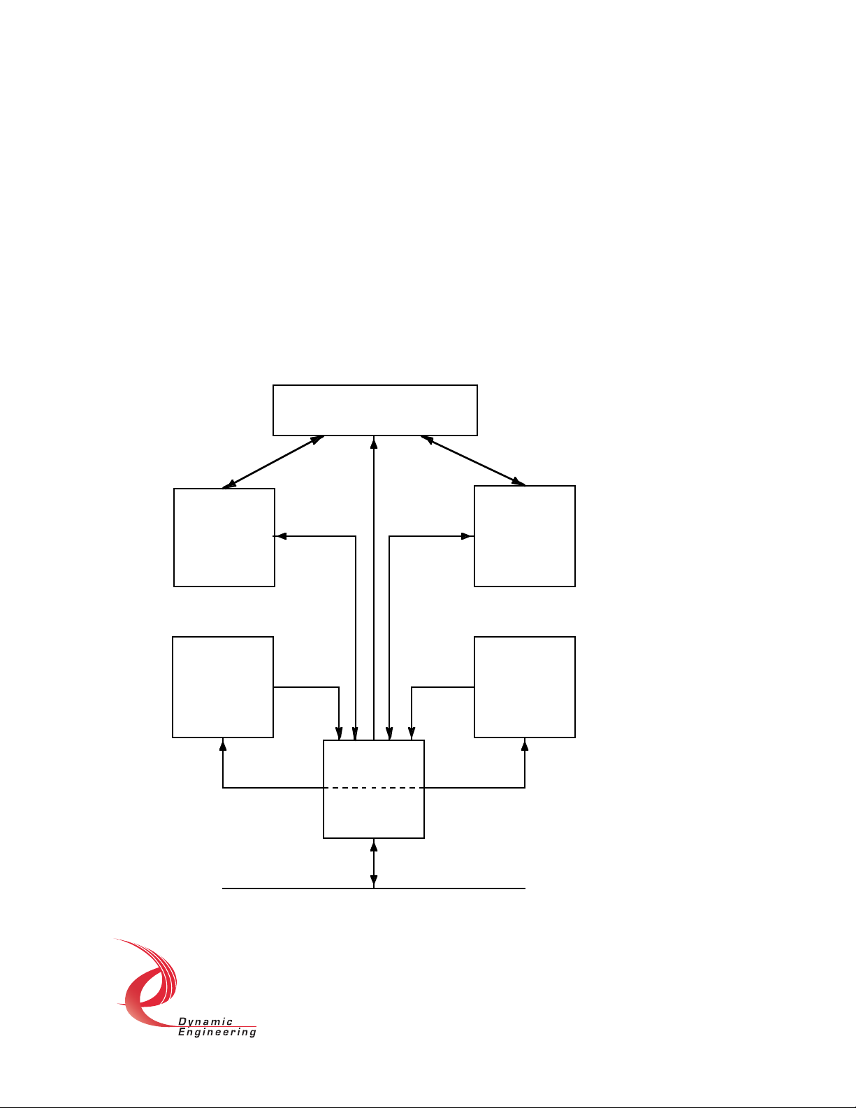
FIGURE 1 PMC BISERIAL-II BLOCK DIAGRAM 6
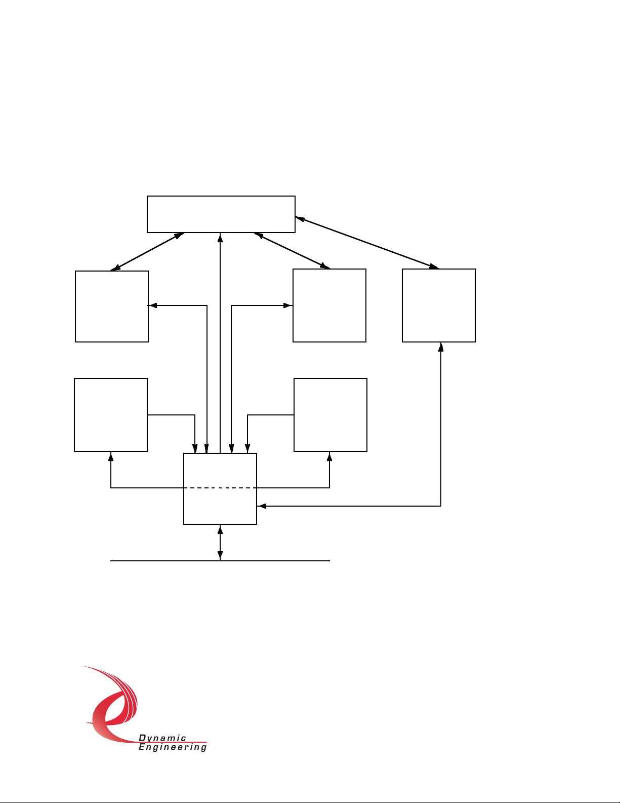
FIGURE 2 PMC BISERIAL-II PS2 BLOCK DIAGRAM 7
FIGURE 3 PS2 TIMING DIAGRAM 11
FIGURE 4 PMC BISERIAL-II PS2 INTERNAL ADDRESS MAP 13
FIGURE 5 PMC BISERIAL-II BASE CONTROL REGISTER BIT MAP 15
FIGURE 6 PMC BISERIAL-II INTERRUPT ENABLE REGISTER BIT MAP 16
FIGURE 7 PMC BISERIAL-II TX CONTROL REGISTER BIT MAP 17
FIGURE 8 PMC BISERIAL-II RX CONTROL REGISTER BIT MAP 18
FIGURE 9 PMC BISERIAL-II PARALLEL OUTPUT DATA BIT MAP 19
FIGURE 10 PMC BISERIAL-II STATUS REG 0 BIT MAP 20
FIGURE 11 PMC BISERIAL-II STATUS 1 BIT MAP 22
FIGURE 12 PMC BISERIAL-II COSEN REGISTER BIT MAP 24
FIGURE 13 PMC BISERIAL-II DIRECTION TERMINATION CONTROL BIT MAP 26
FIGURE 14 PMC BISERIAL-II COSEDGE REGISTER BIT MAP 28
FIGURE 15 PMC BISERIAL-II PN1 INTERFACE 31
FIGURE 16 PMC BISERIAL-II PN2 INTERFACE 32
FIGURE 17 PMC BISERIAL-II FRONT PANEL INTERFACE 33
Hardware and Software Design • Manufacturing Services
P a g e 5
Page 6
Product Description
The PMC BiSerial-II PS2 is part of the PMC Module family of modular I/O
components by Dynamic Engineering. The PMC BiSerial-II is capable of providing
multiple serial protocols. The PS2 protocol implemented provides 4 serially
encoded inputs and outputs plus 8 IO with Change of State interrupt capability.
Other custom interfaces are available. We will redesign the state machines and
create a custom interface protocol. That protocol will then be offered as a
“standard” special order product. Please see our web page for current protocols
offered. Please contact Dynamic Engineering with your custom application.
485 buffers
termination
State
Machine
B
FIFO B
128K x 32
State
Machine
A
FIFO A
128K x 32
Data Flow
Control
PCI IF
FIGURE 1 PMC BISERIAL-II BLOCK DIAGRAM
Hardware and Software Design • Manufacturing Services
P a g e 6
Page 7
The standard configuration shown in Figure one makes use of two external [to the
Xilinx ] FIFOs. The FIFOs can be as large as 128K deep x 32 bits wide. Some
designs do not require so much memory and are more efficiently implemented
using the internal FIFOs.
485 buffers
termination
State
Machine
RX
FIFO RX
128 x 32
x4
x4
Data Flow
Control
PCI IF
State
Machine
TX
FIFO TX
128 x 32
x4
Parallel Port
8 IO
COS Int
x4
FIGURE 2 PMC BISERIAL-II PS2 BLOCK DIAGRAM
The PS2 implementation has 8 - 128 x 32 FIFOs using the internal block RAM of
the Xilinx. Each TX and RX channel has an associated FIFO. The transmit FIFOs
have the option to fill in parallel - if the same data pattern is to be sent from the 4
Hardware and Software Design • Manufacturing Services
P a g e 7
Page 8

ports then the 4 FIFOs can be filled with the same pattern at the same time.
Fewer PCI cycles are required and less processing by the host.
The transmit data rate can be derived from the 20 MHz on-board oscillator. The
normal transmitter data rate is 5 MHz (divide-by 4), other divisors are also
provided. The first COS port can be used as an alternate clock source as well as
the PCI clock. The max clock rate after division is required to be 20 MHz. The
receiver automatically adjusts to data rates.
The FIFOs always operate at the PCI clock frequency of 33 MHz to simplify testing
and operational functions. Loop-back is provided to allow confidence testing of an
installed board.
Thirty-two differential I/O are provided for the serial signals. The drivers and
receivers conform to the RS-485 specification (exceeds RS-422 specification).
The RS-485 input signals are selectively terminated with 100Ω. The termination
resistors are in two-element packages to allow flexible termination options for
custom formats and protocols. Optional pullup/pulldown resistor packs can also
be installed to provide a logic ‘1’ on undriven lines. The terminations and
transceivers are programmable through the Xilinx device to provide the proper
mix of outputs and inputs and terminations needed for a specific protocol
implementation. The COS directions are programmable via software. The Serial
interfaces are pre-programmed to their intended direction. The terminations are
programmable for all IO.
All configuration registers support read and write operations for maximum
software convenience, and all addresses are long word aligned.
The PMC BiSerial-II conforms to the PMC and CMC draft standards. This
guarantees compatibility with multiple PMC Carrier boards. Because the PMC
may be mounted on different form factors, while maintaining plug and software
compatibility, system prototyping may be done on one PMC Carrier board, with
final system implementation on a different one.
The PMC BiSerial-II uses a 10 mm inter-board spacing for the front panel,
standoffs, and PMC connectors. The 10 mm height is the "standard" height and
will work in most systems with most carriers. If your carrier has non-standard
connectors [height] to mate with the PMC BiSerial-II, please let us know. We may
be able to do a special build with a different height connector to compensate.
Hardware and Software Design • Manufacturing Services
P a g e 8
Page 9

The serial channels are each supported by a 128 by 32-bit FIFO. The FIFOs
support long word reads and writes. A full 32-bit path exists for loop-back testing
of each FIFO. Data is latched and the bus immediately released on a write-cycle.
On a read cycle the data is read after the bus is released from the previous read.
This has the effect of adding one extra read to start capturing data, but means
there is no delay in future reads.
The serial format for transmit and receive is 32 bits per word, LSB first. The
data switches on the falling edge of the reference clock and is valid on the rising
edge. The strobe is asserted on the falling edge before the first data bit should
be taken and held on until the falling edge after the last bit. If more than one
word is sent the words are sent back-to-back without a gap.
The transmit data is sent with the clock and strobe. If the receiver operates as
an asynchronous interface then the first data word can be a sync pattern and the
clock and strobe ignored. The receiver on the PS2 utilizes the clock and the
strobe. The clock is free-running.
The serial receive channels can receive continuous or burst data. The host can
poll the FIFO flags or wait for the programmable FIFO interrupt. The message can
then be read over the PCI bus directly from the FIFO.
The Output channels have a separate 128 x 32-bit FIFO each. The FIFO is written
as long words. Normal operation is to load the TX FIFO for the channel of
interest then set the TX Start bit. The data will start to be transmitted at the
programmed rate along with the strobe. The clock will already be running. The
state-machine will continue to read data from the FIFO and transmit until the FIFO
is empty. When the transmission is completed a programmable interrupt can be
set. The start bit is automatically cleared at the end of a transmission.
Various interrupts are supported by the PMC BiSerial-II PS2. An interrupt can be
configured to occur at the end of a transmitted message. An interrupt can be set
at the end of a reception. Interrupts can occur based on the IO. All interrupts are
individually maskable and a master interrupt enable is also provided to disable all
interrupts simultaneously. The current status is available for the FIFOs making it
possible to operate in a polled mode.
Hardware and Software Design • Manufacturing Services
P a g e 9
Page 10

Theory of Operation
The PMC BiSerial-II PS2 is designed for transferring data from one point to
another with a simple serial protocol.
The PMC BiSerial-II PS2 features a Xilinx FPGA. The FPGA contains all of the
registers and protocol controlling elements of the BiSerial II design. Only the
transceivers, and switches are external to the Xilinx device.
The PMC BiSerial-II is a part of the PMC Module family of modular I/O products. It
meets the PMC and CMC draft Standards. In standard configuration, the PMC
BiSerial-II is a Type 1 mechanical with no components on the back of the board
and one slot wide, with 10 mm inter-board height. Contact Dynamic Engineering
for a copy of this specification. It is assumed that the reader is at least casually
familiar with this document and logic design.
The PCI interface to the host CPU is controlled by a logic block within the Xilinx.
The BiSerial II design requires one wait state for read or write cycles to any
address. The PMC BiSerial-II is capable of supporting 40 MBytes per second into
and out of the FIFO's. The wait states refer to the number of clocks after the PCI
core decode before the “terminate with data” state is reached. Two additional
clock periods account for the 1 clock delay to decode the signals from the PCI
bus and to convert the terminate with data state into the TRDY signal.
The BiSerial II can support many protocols. The PMC BiSerial-II PS2 uses serial
encoded LSB first data, clock and strobe. Data is sent in 32 bit words which are
concatenated for multiple word transfers. The timing is shown in the next
diagram.
State machines within the FPGA control all transfers between the interanal FIFO
and FPGA logic, and the FPGA and the data buffers. The TX state machine reads
from the transmit FIFOs and loads the shift registers before sending the data. The
RX state machine receives data from the data buffers and takes care of moving
data from the shift register into the RX FIFOs.
Data is read from the TX FIFOs and loaded into the shift register. The LSB is then
present at the output of the data buffer. One bit period later the data is
Hardware and Software Design • Manufacturing Services
P a g e 10
Page 11
transitioned to the next value. The LSB+1 is now on the data lines. This process
repeats until the first word is transferred. If more data is available from the FIFO,
then the process repeats for the second word. In the standard timing there are
no inter-word gaps, the data stream is continuous from LSB to MSB for a
compact serial transfer. Please refer to the register bit definitions for more
details.
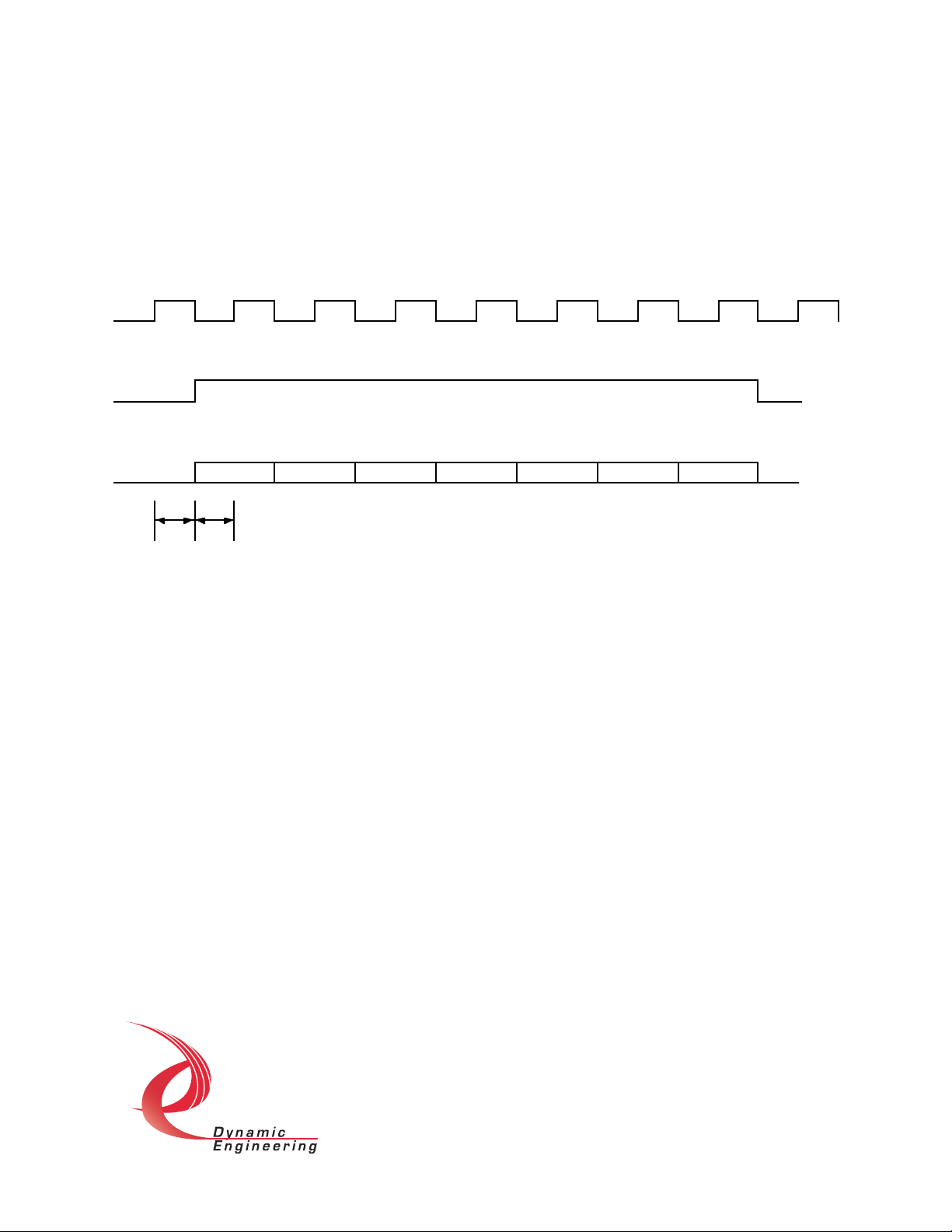
CLK
STB
DATA
1/2T1/2
FIGURE 3 PS2 TIMING DIAGRAM
LSB LSB +1
T
...
MSB LSB
...
MSB
The data rate is set by a 12-bit field in the Txs control register. The data, and
strobe change on the falling edge and are valid on the rising edge. Approximately
1/2 period of set-up and hold are available at the receiver. The transceivers are
rated for 40 MHz. The top rate programmed for the IO is 20 MHz. The Statemachine is designed with the assumption that the PCI clock is faster than the IO
clock rate plus some margin. Faster clock rates are possible with minor changes
to the state-machine / FIFO architecture.
The receive function uses a free running shift register coupled with the receive
state-machine to capture the data. When strobe is detected to have
transitioned from low to high the state-machine starts to count the received
clocks. When the word has been received the data is moved from the shift
register to a parallel holding register. The shift register continues to capture the
next word. The data is moved from the parallel holding register to the RX FIFO
for that channel. When the strobe is detected to be low the receiver clears the
receive enable bit, sets the interrupt if enabled, and goes back to the idle state.
Hardware and Software Design • Manufacturing Services
P a g e 11
Page 12

If the receiver is enabled and a transmission is already in progress, the receiver
will ignore the data until the strobe has been detected to be low then asserted
high again. The design will help to make sure that the hardware stays on 32 bit
data boundaries. If the FIFO is full when the receiver is enabled the state-machine
will wait in the idle state until the FIFO is not full before starting a new reception.
Hardware and Software Design • Manufacturing Services
P a g e 12
Page 13

Address Map
BIS2_BASE 0x0000 // 0 base control register offset
BIS2_TX 0x0004 // 1 tx control register offset
BIS2_TXS 0x0008 // 2 tx special control register offset
BIS2_RX 0x000c // 3 rx control register offset
BIS2_PARDAT 0x0010 // 4 parallel data out register
BIS2_STAT0 0x0014 // 5 status register 0 interrupts tx, rx, rising, falling
BIS2_STAT1 0x0018 // 6 status register 1 parallel data in, fifo status, switch
BIS2_COSEN 0x001C // 7 parallel enable COS register
BIS2_FIFORX0 0x0020 // 8 RX Internal FIFO 0 read-write port
BIS2_FIFORX1 0x0024 // 9 RX Internal FIFO 1 read-write port
BIS2_FIFOTX0 0x0028 // 10 TX Internal FIFO 0 read-write port
BIS2_FIFOTX1 0x002C // 11 TX Internal FIFO 1 read-write port
BIS2_FIFOTX2 0x0030 // 12 TX Internal FIFO 2 read-write port
BIS2_FIFOTX3 0x0034 // 13 TX Internal FIFO 3 read-write port
BIS2_DIR_TERM 0x0038 // 14 direction and termination offset
BIS2_FIFORX2 0x003C // 15 RX Internal FIFO 2 read-write port
BIS2_FIFORX3 0x0040 // 16 RX Internal FIFO 3 read-write port
BIS2_COSEDGE 0x0044 // 17 parallel rising / falling enable register
FIGURE 4 PMC BISERIAL-II PS2 INTERNAL ADDRESS MAP
The address map provided is for the local decoding performed within the PMC
BiSerial-II. The addresses are all offsets from a base address, which is assigned
by the system when the PCI bus is configured.
The VendorId = 0x10EE. The CardId = 0x001D. Current revision = 0x00
Hardware and Software Design • Manufacturing Services
P a g e 13
Page 14

Programming
Programming the PMC BiSerial-II PS2 requires only the ability to read and write
data from the host. The base address is determined during system configuration
of the PCI bus. The base address refers to the first user address for the slot in
which the PMC is installed.
Depending on the software environment it may be necessary to set-up the system
software with the PMC BiSerial-II "registration" data. For example in WindowsNT
there is a system registry, which is used to identify the resident hardware.
In order to receive data the software is only required to enable the Rx FIFO, and
Rx state machine for the channels of interest. To transmit the software will need
to load the message into the appropriate channel FIFO, set the frequency and
enable the transmitter.
The interrupt service routine should be loaded and the interrupt mask set. The
interrupt service routine can be configured to respond to the channel interrupts,
the COS interrupts or both. After the interrupt is received, the data can be
retrieved. An efficient loop can then be implemented to fetch the data. New
messages can be received even as the current one is read from the FIFO.
The TX interrupt indicates to the software that a message has been sent and that
the message has completed. If more than one interrupt is enabled, then the SW
needs to read BIS2_STAT1 to see which source caused the interrupt. The status
bits of BIS2_STAT1 are latched and are explicitly cleared by writing a one to the
corresponding bit. It is a good idea to read the status register and write that
value back to clear all the latched interrupt status bits before starting a transfer.
This will insure that the interrupt status values read by the interrupt service
routine came from the current transfer.
Refer to the Theory of Operation section above and the Interrupts section below
for more information regarding the exact sequencing and interrupt definitions.
Hardware and Software Design • Manufacturing Services
P a g e 14
Page 15

Register Definitions
BIS2_BASE
[$00] BiSerial II Base Control Register Port read/write
CONTROL BASE
DATA BIT DESCRIPTION
31-9 Spare
8 Reset FIFO RX
7-5 spare
4 Reset FIFO TX
3 spare
2 spare
1 Interrupt Set
0 Interrupt Enable Master
FIGURE 5 PMC BISERIAL-II BASE CONTROL REGISTER BIT MAP
All bits are active high and are reset on power-up or reset command.
Interrupt Enable Master when '1' allows interrupts generated by the
PMC-BiSerial-II-PS2 to be driven onto the backplane [INTA]. When '0' the
interrupts can be individually enabled and used for status without driving the
backplane. Polled operation can be performed in this mode.
Interrupt Set when '1' and the Master is enabled, forces an interrupt request.
This feature is useful for testing and software development.
Hardware and Software Design • Manufacturing Services
P a g e 15
Page 16

BIS2_TX
[$04] BiSerial II Transmitter Register Port read/write
CONTROL INTERRUPT ENABLE
DATA BIT DESCRIPTION
31-11 Spare
10 tx load control
9 tx clock control
8 spare
7 int_en_tx3
6 int_en_tx2
5 int_en_tx1
4 int_en_tx0
3 start_tx3
2 start_tx2
1 start_tx1
0 start_tx0
FIGURE 6 PMC BISERIAL-II INTERRUPT ENABLE REGISTER BIT MAP
All bits are active high and are reset on power-up or reset command.
Start_tx0 - 3 when '1' and data is loaded into the corresponding FIFO causes the
transmitter state-machine to begin a data transfer. When the transfer is
complete this bit is auto-cleared. The transmission length is controlled by the
amount of data stored into the FIFO.
Int_en_tx0-3 when '1' the interrupt for the corresponding channel will be asserted
at the completion of a transmission. The master interrupt enable is also required
to be enabled. Please note that the channel status can be read without using
interrupts.
Tx clock control when '1' enables the clocks associated with the transmit
channels to be driven. If the clocks are not used then this bit can remain in the
'0' state. Some interfaces treat the data asynchronously and do not use the
reference clock.
Hardware and Software Design • Manufacturing Services
P a g e 16
Page 17

Tx load control when '1' causes a write to the channel 0 FIFO to load channels
0,1,2,3 with the same data. When '0' the FIFOs are loaded independently.
BIS2_TXs
[$08] BiSerial II Txs Control Register Port read/write
CONTROL TX
DATA BIT DESCRIPTION
31-15 Spare
14-13 reference select
12 output select
11-0 divisor
FIGURE 7 PMC BISERIAL-II TX CONTROL REGISTER BIT MAP
Reference Select:
when 00 or 01 selects the oscillator = 20 MHz
when 10 the external reference is selected [IO 24]
when 11 the PCI clock is selected
The reference selected is divided using the selected divisor and then divided in half
for a 50% duty cycle reference clock. F = R/2*(D+1). Where F = the frequency
desired, R = the selected reference frequency, and D = the specified divisor. For
example to create a 5 MHz transmit frequency from the standard 20 MHz
oscillator a divide by 4 is needed. The divisor is 0x01.
The output select when '1' selects the output from the divider. When '0' the
selected reference frequency is used. If the clock programmed is not driven to
the output please check the tx clock control in the TX register.
Hardware and Software Design • Manufacturing Services
P a g e 17
Page 18

BIS2_RX
[$0C] BiSerial II Rx Control Register Port read/write
CONTROL RX
DATA BIT DESCRIPTION
31-12 Spare
11 loop_back3
10 loop_back2
9 loop_back1
8 loop_back0
7 int_en_rx3
6 int_en_rx2
5 int_en_rx1
4 int_en_rx0
3 start_rx3
2 start_rx2
1 start_rx1
0 start_rx0
FIGURE 8 PMC BISERIAL-II RX CONTROL REGISTER BIT MAP
Start_rx0-3 when '1' enables the receiver state machine to receive messages. If
Start_rx0-3 is set to a zero the reception will stop after the current word is
stored in the FIFO. Start_rx0-3 is auto-cleared at the end of a reception.
Int_en_rx0-3 when '1' the interrupt for the corresponding channel will be asserted
at the completion of a reception. The master interrupt enable is also required to
be enabled. Please note that the channel status can be read without using
interrupts.
Loop-back0-3 when '1' enables the receiver FIFO for that channel to be loaded
from the PCI bus instead of the receiver state-machine. Loop-back testing can be
accomplished with the FIFOs.
Hardware and Software Design • Manufacturing Services
P a g e 18
Page 19

BIS2_PARDAT
[$10] BiSerial II Parallel Data Output Register read/write
CONTROL UART
DATA BIT DESCRIPTION
31-8 Spare
7-0 parallel output data
FIGURE 9 PMC BISERIAL-II PARALLEL OUTPUT DATA BIT MAP
There are 8 potential output bits in the parallel port. The Direction and
Termination register sets the direction of the bits. When the direction is set to
output the bit definitions from this register are driven onto the corresponding
parallel port lines.
This port is direct read-write of the register. The IO side is read-back from the
Status1 port also the lowest 8 bits. It is possible that the output data does not
match the IO data in the case of the Direction bits being set to input.
Hardware and Software Design • Manufacturing Services
P a g e 19
Page 20

BIS2_STAT0
[$14] BiSerial II Status Port 0 read status, write clear
STATUS 0
DATA BIT DESCRIPTION
31-25 Spare
24 interrupt status
23 f7_intr_lat
22 f6_intr_lat
21 f5_intr_lat
20 f4_intr_lat
19 f3_intr_lat
18 f2_intr_lat
17 f1_intr_lat
16 f0_intr_lat
15 r7_intr_lat
14 r6_intr_lat
13 r5_intr_lat
12 r4_intr_lat
11 r3_intr_lat
10 r2_intr_lat
9r1_intr_lat
8r0_intr_lat
7 rx3_intr_lat
6 rx2_intr_lat
5 rx1_intr_lat
4 rx0_intr_lat
3 tx3_intr_lat
2 tx2_intr_lat
1 tx1_intr_lat
0 tx0_intr_lat
FIGURE 10 PMC BISERIAL-II STATUS REG 0 BIT MAP
When Interrupt Status is read as a one, it indicates that one or more latched
interrupt conditions are true. In order for an actual system interrupt to occur, the
interrupt enable for that condition and the Master Interrupt Enable must both be
asserted. When this bit is zero, no interrupt conditions are pending.
Hardware and Software Design • Manufacturing Services
P a g e 20
Page 21

The interrupt conditions are latched and held in special interrupt status latches.
The latched signals are made available on the Bis2_stat0 port. The latched bits
remain set until the corresponding bit is written back to the port. When an
interrupt occurs or if polling is used this port can be used to determine which
channel requires attention. The active channel should be taken care of and then
the bit set to clear the request. The combination of port access and bit position
set is used to clear the bit. No second write is required to re-enable the latching
mechanism.
Tx0-3_intr_lat is set when the transmitter completes a transfer. To use as an
interrupt the Tx_Int_En0-3 [Bis2_TX] must also be set as well as the master
interrupt enable.
Rx0-3_intr_lat is set when the receiver completes a reception. To use as an
interrupt the Rx_Int_En0-3 [Bis2_RX] must also be set as well as the master
interrupt enable.
R0-7_intr_lat is set when the parallel port bit has received a rising transition
0->1. To use as an interrupt the par_int_en_r0-7 [Bis2_COSEN] must also be set
as well as the master interrupt enable.
F0-7_intr_lat is set when the parallel port bit has received a falling transition
1->0. To use as an interrupt the par_int_en_f0-7 [Bis2_COSEN] must also be set
as well as the master interrupt enable.
Hardware and Software Design • Manufacturing Services
P a g e 21
Page 22

BIS2_STAT1
[$18] BiSerial II Status Port 1 read only
FIFO Status, Parallel Data In & Switch Register
DATA BIT DESCRIPTION
31-24 sw7-0
23 rx_fifo_full3
22 rx_fifo_full2
21 rx_fifo_full1
20 rx_fifo_full0
19 rx_fifo_mt3
18 rx_fifo_mt2
17 rx_fifo_mt1
16 rx_fifo_mt0
15 tx_fifo_full3
14 tx_fifo_full2
13 tx_fifo_full1
12 tx_fifo_full0
11 tx_fifo_mt3
10 tx_fifo_mt2
9 tx_fifo_mt1
8 tx_fifo_mt0
7-0 dat_in7-0
FIGURE 11 PMC BISERIAL-II STATUS 1 BIT MAP
The Switch Read Port has the user bits. The user bits are connected to the eight
dip-switch positions. The switches allow custom configurations to be defined by
the user and for the software to identify a particular board by its switch settings
and to configure it accordingly.
The Dip-switch is marked on the silk-screen with the positions of the digits and the
1
0
'1' and '0' definitions. The numbers are hex coded. The
example shown would produce 0x12 when read [and shifted
down] from the BIS2_STAT1 port.
70
Tx_fifo_mt3-0 is '1' when the Transmit FIFO is empty for that channel. When data
Hardware and Software Design • Manufacturing Services
P a g e 22
Page 23

is stored in the FIFO the status will be '0'.
Tx_fifo_full3-0 is '1' when the Transmit FIFO is full for that channel. When there is
less than a full FIFO the status will be '0'.
Rx_fifo_mt3-0 is '1' when the Receive FIFO is empty for that channel. When data
is stored in the FIFO the status will be '0'.
Rx_fifo_full3-0 is '1' when the Receive FIFO is full for that channel. When there is
less than a full FIFO the status will be '0'.
Dat_in is the parallel data read from the parallel port. Each bit is re-synchronized
to the PCI clock and presented without further filtering. Read the state of the
parallel port lines from this port. Please use the COS input features to capture
transitions. Please note that the input port is independent of the port direction.
If the port is defined to be an output then reading this port will return the Parallel
Data output definition. If the direction is input then this port will return the state
of the IO lines and may not match the parallel output data definition.
Hardware and Software Design • Manufacturing Services
P a g e 23
Page 24

BIS2_COSEN
[$1C] BiSerial II Parallel Enable COS register
Parallel Enable Change of State Register
DATA BIT DESCRIPTION
31-24 spare
23-16 par_int_en_f
15-8 par_int_en_r
7-0 par_en7-0
FIGURE 12 PMC BISERIAL-II COSEN REGISTER BIT MAP
Par_en bits 7-0 correspond to the parallel IO port bits. When set the COS
function is enabled for that input bit. Normally the par_en bit will not be enabled
for ports defined to be outputs. Once enabled, the state-machine will continue to
process COS until disabled by setting to '0'. The state-machine will return to the
idle state and wait to be enabled again. Disabling the COS detector will not affect
previously captured status in Stat0. That will have to be cleared explicitly.
Par_int_en_r bits 7-0 correspond to the parallel IO port bits. If the par_en is set
and a rising edge is detected for the IO line(s) enabled then the interrupt is
triggered to the host. The master enable is also required. The corresponding
Rising bit must also be set. The status register [Stat0] will capture the event
even if the interrupt is not enabled to allow polled operation.
Par_int_en_f bits 7-0 correspond to the parallel IO port bits. If the par_en is set
and a falling edge is detected for the IO line(s) enabled then the interrupt is
triggered to the host. The master enable is also required. The corresponding
Falling bit must also be set. The status register [Stat0] will capture the event
even if the interrupt is not enabled to allow polled operation.
Hardware and Software Design • Manufacturing Services
P a g e 24
Page 25

BIS2_FIFOTX0-3
[$28,2C,30,34] BiSerial II Tx FIFO write-read port
The BiSerial II supports 32-bit writes to the transmit data FIFO. Data is aligned
D31-0. Normally this port is only written to, but for loop-back testing the contents
of the FIFO can be read out over the PCI bus. The data is moved from the FIFO to
the holding register at the end of a read cycle. The first read will return whatever
is in the holding register, the second will return the first data… The engineering
kit contains software, which performs a Tx FIFO loop-back test on each channel.
Once data is read from the FIFO it is no longer available for transmission. There
is a bit in the BIS2_TX register which causes the data written to channel 0 to also
be written to channels 1,2, and 3. If the same data is to be transmitted out of
each port this feature can save 3 FIFO fill operations.
BIS2_FIFORX0-3
[$20,24,3C,40] BiSerial II Rx FIFO write-read port
The BiSerial II supports 32-bit reads from the receive data FIFO. Data is aligned
D31-0. Normally this port is only read from, but for loop-back testing the contents
of the FIFO can be written from the PCI bus. The FIFO loop back bit in the Rx
control register must be set to a '1' in order to accomplish this. The engineering
kit contains software, which performs an Rx FIFO loop-back test. Once data is
read from the FIFO it is no longer available.
The data path from the FIFO to the host is pipelined through a holding register.
After reset or a condition where the last read of the FIFO holding register
happened with an empty FIFO a pre-read will be required to move data from the
FIFO to the holding register. In most cases, with messages completely stored
within the FIFO, this will equate to one pre-read followed by the message count
reads to retrieve the stored message.
Hardware and Software Design • Manufacturing Services
P a g e 25
Page 26

BIS2_DIR_TERM
[$38] BiSerial II Direction and Termination Register Port read/write
CONTROL DIR_TERM REGISTER
DATA BIT DESCRIPTION
13-0 DIRection 13-0 0 = read 1 = drive
29-16 TERMination 13-0 1 = terminated
FIGURE 13 PMC BISERIAL-II DIRECTION TERMINATION CONTROL BIT MAP
The direction for each of the 32 differential pairs is controlled through this port.
The port defaults to zero, which corresponds to tri-stating the drivers and no
terminations enabled.
Pull-up and Pull-down resistors built into some '485 interface devices may make
the signal appear to be driven (if open) when in the tri-stated mode. Enabling the
termination on a tri-stated line will yield approximately 2.5V on each side of the tristated driver.
The base design of the PMC_BiSerial II_PS2 sets direction bits 0-8 high (outputs),
and direction bits 9-11 low (inputs). Currently the forced bits are read-write but
have no effect. Bits 12 and 13 are used to control the parallel port bits.
CONTROL CORRESPONDING IO BIT(S)
DIR_0..7 IO_0..7
DIR8 IO_8..11
DIR9 IO_12..15
DIR10 IO_16..19
DIR11 IO_20..23
DIR12 IO_24..27
DIR13 IO_28..31
Parallel termination resistors are supplied on each differential pair along with a
switch to allow the user to select which lines are terminated and where. In some
systems it will make sense to terminate the lines in the cable and in others it will
make sense to use the onboard terminations.
Hardware and Software Design • Manufacturing Services
P a g e 26
Page 27

The terminations for the receive groups should be set to terminate with the user
software in most cases. [term_9 - term_11] If the Parallel Port is set to be an
input with the direction bits then the corresponding termination bits should also
be set.
CONTROL CORRESPONDING IO BIT(S)
TERM_0..7 IO_0..7
TERM_8 IO_8..11
TERM_9 IO_12..15
TERM_10 IO_16..19
TERM_11 IO_20..23
TERM_12 IO_24..27
TERM_13 IO_28..31
Hardware and Software Design • Manufacturing Services
P a g e 27
Page 28

BIS2_COSEDGE
[$44] BiSerial II COS Edge Definition Register
Change of State Edge Register
DATA BIT DESCRIPTION
31-16 Spare
15-8 falling7-0
7-0 rising7-0
FIGURE 14 PMC BISERIAL-II COSEDGE REGISTER BIT MAP
Rising when set for a channel enables that COS state-machine [if enabled] to look
for rising edge transitions and to set the status bit when found.
Falling when set for a channel enables that COS state-machine [if enabled] to look
for falling edge transitions and to set the status bit when found.
The COS state machine operates at the PCI frequency and can handle single width
pulse transitions. If a signal goes from low to high to low on successive clocks
then both edges will be found if the COS is enabled and the rising and falling bits
are set. The state-machine can be altered if the user wants to have some
filtering action employed. There is plenty of room in the FPGA for adding
minimum count processing etc. Please contact Dynamic Engineering with your
requirements.
Hardware and Software Design • Manufacturing Services
P a g e 28
Page 29

Interrupts
PMC BiSerial-II interrupts are treated as auto-vectored. When the software
enters into an exception handler to deal with a PMC BiSerial-II interrupt the
software must read the status register to determine the cause(s) of the interrupt,
clear the interrupt request(s) and process accordingly. Power on initialization will
provide a cleared interrupt request and interrupts disabled.
For example, the PMC BiSerial-II Tx state machine generates an interrupt request
when a transmission is complete and the Tx int enable and Master interrupt
enable bits are set. The transmission is considered complete when the last bit is
output from the output shift register.
The interrupt is mapped to INTA on the PMC connector, which is mapped to a
system interrupt when the PCI bus configures. The source of the interrupt is
obtained by reading BIS2_STAT0. The status remains valid until that bit in the
status register is explicitly cleared.
When an interrupt occurs, the Master interrupt enable should be cleared and the
status register read to determine the cause of the interrupt. Next perform any
processing needed to remove the interrupting condition, clear the latched bit and
set the Master interrupt enable bit high again.
The individual enables operate after the interrupt holding latches, which store the
interrupt conditions for the CPU. This allows for operating in polled mode simply
by monitoring the BIS2_STAT0 register. Alternatively, the conditions of interest
can be enabled, but the Master interrupt enable left disabled. Then the interrupt
status bit in BIS2_STAT0 can be monitored. If one of the enabled conditions
occurs, the interrupt status bit will be set, but unless the Master interrupt enable
is set, a system interrupt will not occur.
Hardware and Software Design • Manufacturing Services
P a g e 29
Page 30

Loop-back
The Engineering kit has reference software, which includes an external loop-back
test. The PS2 version of the PMC-BiSerial II utilizes a 68 pin SCSI II front panel
connector. The test requires an external cable with the following pins connected.
SIGNALs + - + -
Tx/Rx Clock 0 9 43 28 62
Tx/Rx Data 0 7 41 21 55
Tx/Rx Strobe 0 11 45 3 37
Tx/Rx Clock 1 1 35 30 64
Tx/Rx Data 1 14 48 22 56
Tx/Rx Strobe 1 6 40 5 39
Tx/Rx Clock 2 2 36 32 66
Tx/Rx Data 2 16 50 24 58
Tx/Rx Strobe 2 12 46 8 42
Tx/Rx Clock 3 4 38 34 68
Tx/Rx Data 3 17 51 26 60
Tx/Rx Strobe 3 19 53 10 44
Parallel Port
P0 - P4 13 47 23 57
P1 - P5 15 49 25 59
P2 - P6 18 52 27 61
P3 - P7 20 54 29 63
Hardware and Software Design • Manufacturing Services
P a g e 30
Page 31

PMC PCI Pn1 Interface Pin Assignment
The figure below gives the pin assignments for the PMC Module PCI Pn1 Interface
on the PMC BiSerial-II-IO. See the User Manual for your carrier board for more
information. Unused pins may be assigned by the specification and not needed by
this design.
-12V[unused] 1 2
GND INTA# 3 4
56
BUSMODE1# +5V 7 8
910
GND - 11 12
CLK GND 13 14
GND - 15 16
+5V 17 18
AD31 19 20
AD28- AD27 21 22
AD25- GND 23 24
GND - C/BE3# 25 26
AD22- AD21 27 28
AD19 +5V 29 30
AD17 31 32
FRAME#- GND 33 34
GND IRDY# 35 36
DEVSEL# +5V 37 38
GND LOCK# 39 40
41 42
PAR GND 43 44
AD15 45 46
AD12- AD11 47 48
AD9- +5V 49 50
GND - C/BE0# 51 52
AD6- AD5 53 54
AD4 GND 55 56
AD3 57 58
AD2- AD1 59 60
+5V 61 62
GND 63 64
FIGURE 15 PMC BISERIAL-II PN1 INTERFACE
Hardware and Software Design • Manufacturing Services
P a g e 31
Page 32

PMC PCI Pn2 Interface Pin Assignment
The figure below gives the pin assignments for the PMC Module PCI Pn2 Interface
on the PMC BiSerial-II-IO. See the User Manual for your carrier board for more
information. Unused pins may be assigned by the specification and not needed by
this design.
+12V[unused] 1 2
34
GND 5 6
GND 7 8
910
11 12
RST# BUSMODE3# 13 14
BUSMODE4# 15 16
GND 17 18
AD30 AD29 19 20
GND AD26 21 22
AD24 23 24
IDSEL AD23 25 26
AD20 27 28
AD18 29 30
AD16 C/BE2# 31 32
GND 33 34
TRDY# 35 36
GND STOP# 37 38
PERR# GND 39 40
SERR# 41 42
C/BE1# GND 43 44
AD14 AD13 45 46
GND AD10 47 48
AD8 49 50
AD7 51 52
53 54
GND 55 56
57 58
GND 59 60
61 62
GND 63 64
FIGURE 16 PMC BISERIAL-II PN2 INTERFACE
Hardware and Software Design • Manufacturing Services
P a g e 32
Page 33

BiSerial II Front Panel IO Pin Assignment
The figure below gives the pin assignments for the PMC Module IO Interface on
the PMC BiSerial-II. Also, see the User Manual for your carrier board for more
information. GND* is a plane which is tied to GND through a 1206 0Ω resistor.
DC, AC or open are options. For customized version, or other options, contact
Dynamic Engineering.
IO_0p [tx_clk_1p] IO_0m [tx_clk_1m] 1 35
IO_1p [tx_clk_2p] IO_1m [tx_clk_2m] 2 36
IO_20p [rx_stb_0p] IO_20m [rx_stb_0m] 3 37
IO_2p [tx_clk_3p] IO_2m [tx_clk_3m] 4 38
IO_21p [rx_stb_1p] IO_21m [rx_stb_1m] 5 39
IO_3p [tx_stb_1p] IO_3m [tx_stb_1m] 6 40
IO_4p [tx_dta_0p] IO_4m [tx_dta_0p] 7 41
IO_22p [rx_stb_2p] IO_22m [rx_stb_2m] 8 42
IO_5p [tx_clk_0p] IO_5m [tx_clk_0p] 9 43
IO_23p [rx_stb_3p] IO_23m [rx_stb_3m] 10 44
IO_6p [tx_stb_0p] IO_6m [tx_stb_0m] 11 45
IO_7p [tx_stb_2p] IO_7m [tx_stb_2m] 12 46
IO_24p [par_0p] IO_24m [par_0p] 13 47
IO_8p [tx_dta_1p] IO_8m [tx_dta_1p] 14 48
IO_25p [par_1p] IO_25m [par_1m] 15 49
IO_9p [tx_dta_2p] IO_9m [tx_dta_2p] 16 50
IO_10p [tx_dta_3p] IO_10m [tx_dta_3p] 17 51
IO_26p [par_2p] IO_26m [par_2m] 18 52
IO_11p [tx_stb_3p] IO_11m [tx_stb_3m] 19 53
IO_27p [par_3p] IO_27m [par_3m] 20 54
IO_12p [rx_dta_0p] IO_12m [rx_dta_0m] 21 55
IO_13p [rx_dta_1p] IO_13m [rx_dta_1m] 22 56
IO_28p [par_4p] IO_28m [par_4p] 23 57
IO_14p [rx_dta_2p] IO_14m [rx_dta_2m] 24 58
IO_29p [par_5p] IO_29m [par_5m] 25 59
IO_15p [rx_dta_3p] IO_15m [rx_dta_3m] 26 60
IO_30p [par_6p] IO_30m [par_6m] 27 61
IO_16p [rx_clk_0p] IO_16m [rx_clk_0p] 28 62
IO_31p [par_7p] IO_31m [par_7m] 29 63
IO_17p [rx_clk_1p] IO_17m [rx_clk_1m] 30 64
GND* GND* 31 65
IO_18p [rx_clk_2p] IO_18m [rx_clk_2m] 32 66
GND* GND* 33 67
IO_19p [rx_clk_3p] IO_19m [rx_clk_3m] 34 68
FIGURE 17 PMC BISERIAL-II FRONT PANEL INTERFACE
Hardware and Software Design • Manufacturing Services
P a g e 33
Page 34

Applications Guide
Interfacing
The pin-out tables are displayed with the pins in the same relative order as the
actual connectors. The pin definitions are defined with noise immunity in mind.
The pairs are chosen to match standard SCSI II/III cable pairing to allow a low
cost commercial cable to be used for the interface.
Some general interfacing guidelines are presented below. Do not hesitate to
contact the factory if you need more assistance.
Watch the system grounds. All electrically connected equipment should have a
fail-safe common ground that is large enough to handle all current loads without
affecting noise immunity. Power supplies and power-consuming loads should all
have their own ground wires back to a common point.
Power all system power supplies from one switch. Connecting external voltage to
the PMC BiSerial-II when it is not powered can damage it, as well as the rest of
the host system. This problem may be avoided by turning all power supplies on
and off at the same time. Alternatively, the use of OPTO-22 isolation panels is
recommended.
Keep cables short. Flat cables, even with alternate ground lines, are not suitable
for long distances. The PMC BiSerial-II does not contain special input protection.
The connector is pinned out for a standard SCSI II/III cable to be used. The
twisted pairs are defined to match up with the BiSerial II pin definitions. It is
suggested that this standard cable be used for most of the cable run.
Terminal Block. We offer a high quality 68-screw terminal block that directly
connects to the SCSI II/III cable. The terminal block can mount on standard DIN
rails. HDEterm68
[ http://www.dyneng.com/HDEterm68.html]
We provide the components. You provide the system. Safety and reliability can be
achieved only by careful planning and practice. Inputs can be damaged by static
discharge, or by applying voltage outside of the RS-485 devices rated voltages.
Hardware and Software Design • Manufacturing Services
P a g e 34
Page 35

Construction and Reliability
PMC Modules were conceived and engineered for rugged industrial environments.
The PMC BiSerial-II is constructed out of 0.062 inch thick FR4 material.
Through hole and surface mounting of components are used. IC sockets use
screw machine pins. High insertion and removal forces are required, which
assists in the retention of components. If the application requires unusually high
reliability or is in an environment subject to high vibration, the user may solder the
corner pins of each socketed IC into the socket, using a grounded soldering iron.
The PMC connectors are rated at 1 Amp per pin, 100 insertion cycles minimum.
These connectors make consistent, correct insertion easy and reliable.
The PMC is secured against the carrier with four screws attached to the 2 standoffs and 2 locations on the front panel. The four screws provide significant
protection against shock, vibration, and incomplete insertion.
The PMC Module provides a low temperature coefficient of 2.17 W/oC for
uniform heat. This is based upon the temperature coefficient of the base FR4
material of 0.31 W/m-oC, and taking into account the thickness and area of the
PMC. The coefficient means that if 2.17 Watts are applied uniformly on the
component side, then the temperature difference between the component side
and solder side is one degree Celsius.
Thermal Considerations
The BiSerial II design consists of CMOS circuits. The power dissipation due to
internal circuitry is very low. It is possible to create a higher power dissipation
with the externally connected logic. If more than one Watt is required to be
dissipated due to external loading then forced air cooling is recommended. With
the one degree differential temperature to the solder side of the board external
cooling is easily accomplished.
Hardware and Software Design • Manufacturing Services
P a g e 35
Page 36

Warranty and Repair
Please refer to the warranty page on our website for the current warranty offered
and options.
http://www.dyneng.com/warranty.html
Service Policy
Before returning a product for repair, verify as well as possible that the
suspected unit is at fault. Then call the Customer Service Department for a
RETURN MATERIAL AUTHORIZATION (RMA) number. Carefully package the unit,
in the original shipping carton if this is available, and ship prepaid and insured with
the RMA number clearly written on the outside of the package. Include a return
address and the telephone number of a technical contact. For out-of-warranty
repairs, a purchase order for repair charges must accompany the return.
Dynamic Engineering will not be responsible for damages due to improper
packaging of returned items. For service on Dynamic Engineering Products not
purchased directly from Dynamic Engineering, contact your reseller. Products
returned to Dynamic Engineering for repair by other than the original customer
will be treated as out-of-warranty.
Out of Warranty Repairs
Out of warranty repairs will be billed on a material and labor basis. The current
minimum repair charge is $100. Customer approval will be obtained before
repairing any item if the repair charges will exceed one half of the quantity one list
price for that unit. Return transportation and insurance will be billed as part of
the repair and is in addition to the minimum charge.
For Service Contact:
Customer Service Department
Dynamic Engineering
435 Park Dr.
Ben Lomond, CA 95005
831-336-8891
831-336-3840 fax support@dyneng.com
Hardware and Software Design • Manufacturing Services
P a g e 36
Page 37

Specifications
Host Interface: [PMC] PCI Mezzanine Card - 32 bit
Serial Interface: 4 Tx and 4 Rx serial interfaces each with Data, Clock, Stb. 32 bit word
size, LSB first, multiple words
Tx Data rates generated: 20 MHz oscillator, PCI clock or external clock references with
programmable 12 bit divider for programmable frequencies. Max transmit
and receive rate of 20 MHz with current VHDL. Custom oscillators can be
installed for alternate frequencies.
Rx Data rates accepted: Continuous up to 20 MHz.
Software Interface: Control Registers, Status Ports, FIFOs
Initialization: Hardware Reset forces all registers to 0.
Access Modes: LW boundary Space (see memory map)
Wait States: 1 for all addresses
Interrupt: Tx interrupt at end of transmission [4]
Rx interrupt at end of reception [4]
Change of state interrupts [16]
Software interrupt
DMA: No DMA Support implemented at this time
Onboard Options: All Options are Software Programmable
Interface Options: 68 pin twisted pair cable
68 screw terminal block interface
Dimensions: Standard Single PMC Module.
Construction: FR4 Multi-Layer Printed Circuit, Through Hole and Surface Mount
Components. Programmable parts are socketed.
Temperature Coefficient: 2.17 W/oC for uniform heat across PMC
Power: Max. TBD mA @ 5V
Hardware and Software Design • Manufacturing Services
P a g e 37
Page 38

Order Information
PMC BiSerial-II PS2 PMC Module with 4 TX serial channels, 4 Rx serial
channels, 8 bit parallel port with COS interrupt capability.
RS-485 IO. 32 bit data interface
Eng Kit–PMC BiSerial-II HDEterm68 - 68 position screw terminal adapter
http://www.dyneng.com/HDEterm68.html
HDEcabl68 - 68 IO twisted pair cable
http://www.dyneng.com/HDEcabl68.html
Technical Documentation,
1. PMC BiSerial-II Schematic
2. PMC BiSerial-II PS2 Reference test software
Data sheet reprints are available from the manufacturer’s
web site
reference software: C souirce code requires WinRT.
Note: The Engineering Kit is strongly recommended for first time
PMC BiSerial-II
purchases.
Schematics
Schematics are provided as part of the engineering kit for customer
. This information was current at the time the printed circuit board was last
only
revised. This revision letter is shown on the front of this manual as
“Corresponding Hardware Revision.” This information is not necessarily current or
complete manufacturing data, nor is it part of the product specification.
All information provided is Copyright Dynamic Engineering
reference
Hardware and Software Design • Manufacturing Services
P a g e 38
 Loading...