

Page 1
DYNAMIC ENGINEERING
150 DuBois, Suite C
Santa Cruz, CA 95060
(831) 457-8891 Fax (831) 457-4793
http://www.dyneng.com
sales@dyneng.com
Est. 1988
User Manual
PMC-BISERIAL-III RL1
Eight-Channel UART Interface
PMC Module
Revision A
Corresponding Hardware: Revision D
10-2005-0204
Corresponding Firmware: Revision A
Page 2

Embedded Solutions Page 2 of 37
PMC-BiSerial-III RL1
Eight-Channel
PMC Based UART Interface
Dynamic Engineering
150 DuBois, Suite C
Santa Cruz, CA 95060
(831) 457-8891
FAX: (831) 457-4793
This document contains information of
proprietary interest to Dynamic Engineering. It
has been supplied in confidence and the
recipient, by accepting this material, agrees that
the subject matter will not be copied or
reproduced, in whole or in part, nor its contents
revealed in any manner or to any person except
to meet the purpose for which it was delivered.
Dynamic Engineering has made every effort to
ensure that this manual is accurate and
complete. Still, the company reserves the right
to make improvements or changes in the
product described in this document at any time
and without notice. Furthermore, Dynamic
Engineering assumes no liability arising out of
the application or use of the device described
herein.
The electronic equipment described herein
generates, uses, and can radiate radio
frequency energy. Operation of this equipment
in a residential area is likely to cause radio
interference, in which case the user, at his own
expense, will be required to take whatever
measures may be required to correct the
interference.
Dynamic Engineering’s products are not
authorized for use as critical components in life
support devices or systems without the express
written approval of the president of Dynamic
Engineering.
Connection of incompatible hardware is likely to
cause serious damage.
©2005-2009 by Dynamic Engineering.
Other trademarks and registered trademarks are owned by their respective
manufactures.
Manual Revision A1 Revised October 19,2009
Page 3

Embedded Solutions Page 3 of 37
Table of Contents
PRODUCT DESCRIPTION 6
THEORY OF OPERATION 9
PROGRAMMING 11
ADDRESS MAP 12
Register Definitions 14
RL1_BASE_CONTROL 14
RL1_USER_SWITCH 15
RL1_CHAN_0-7_CONTROL 16
RL1_CHAN_0-7_STATUS 18
RL1_CHAN_0-7_WR_DMA_PNTR 21
RL1_CHAN_0-7_TX_FIFO_COUNT 21
RL1_CHAN_0-7_RD_DMA_PNTR 22
RL1_CHAN_0-7_RX_FIFO_COUNT 22
RL1_CHAN_0-7_FIFO 23
RL1_CHAN_0-7_TX_AMT_LVL 23
RL1_CHAN_0-7_RX_AFL_LVL 23
RL1_CHAN_0-7_TX_CONTROL 24
RL1_CHAN_0-7_RX_CONTROL 25
RL1_CHAN_0-7_TX_START_LATCH 27
RL1_CHAN_0-7_RX_START_LATCH 27
RL1_CHAN_0-7_RX_BYTE_COUNT 28
Loop-back 29
PMC PCI PN1 INTERFACE PIN ASSIGNMENT 30
PMC PCI PN2 INTERFACE PIN ASSIGNMENT 31
FRONT PANEL I/O PIN ASSIGNMENT 32
APPLICATIONS GUIDE 33
Interfacing 33
CONSTRUCTION AND RELIABILITY 34
Page 4

Embedded Solutions Page 4 of 37
THERMAL CONSIDERATIONS 34
WARRANTY AND REPAIR 34
Service Policy 35
Out of Warranty Repairs 35
For Service Contact: 35
SPECIFICATIONS 36
ORDER INFORMATION 37
SCHEMATICS 37
Page 5

Embedded Solutions Page 5 of 37
List of Figures
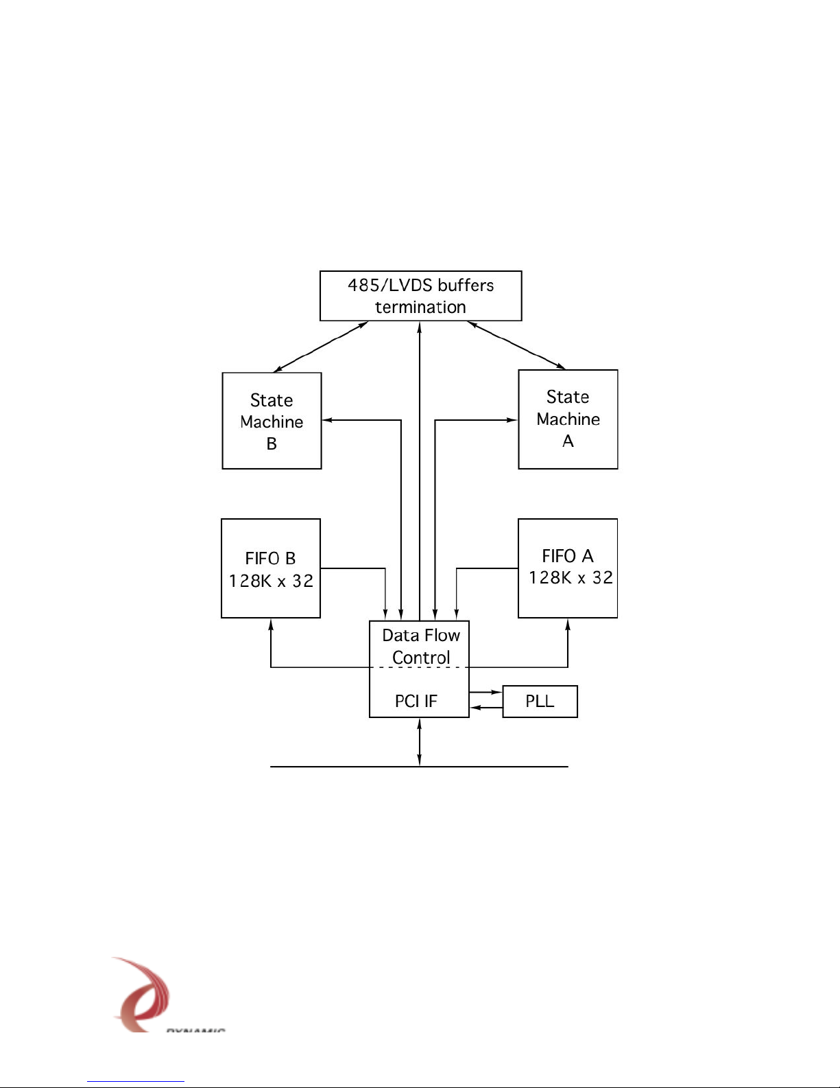
FIGURE 1 PMC-BISERIAL-III BLOCK DIAGRAM 6
FIGURE 2 PMC-BISERIAL-III RL1 BLOCK DIAGRAM 7
FIGURE 3 PMC-BISERIAL-III RL1 XILINX ADDRESS MAP 13
FIGURE 4 PMC-BISERIAL-III RL1 BASE CONTROL REGISTER 14
FIGURE 5 PMC-BISERIAL-III RL1 USER SWITCH PORT 15
FIGURE 6 PMC-BISERIAL-III RL1 CHANNEL CONTROL REGISTER 16
FIGURE 7 PMC-BISERIAL-III RL1 CHANNEL STATUS PORT 18
FIGURE 8 PMC-BISERIAL-III RL1 WRITE DMA POINTER REGISTER 21
FIGURE 9 PMC-BISERIAL-III RL1 TX FIFO DATA COUNT PORT 21
FIGURE 10 PMC-BISERIAL-III RL1 READ DMA POINTER REGISTER 22
FIGURE 11 PMC-BISERIAL-III RL1 RX FIFO DATA COUNT PORT 22
FIGURE 12 PMC-BISERIAL-III RL1 RX/TX FIFO PORT 23
FIGURE 13 PMC-BISERIAL-III RL1 TX ALMOST EMPTY LEVEL REGISTER 23
FIGURE 14 PMC-BISERIAL-III RL1 RX ALMOST FULL LEVEL REGISTER 23
FIGURE 15 PMC-BISERIAL-III RL1 TX CONTROL REGISTER 24
FIGURE 16 PMC-BISERIAL-III RL1 RX CONTROL REGISTER 25
FIGURE 17 PMC-BISERIAL-III RL1 TX START LATCH 27
FIGURE 18 PMC-BISERIAL-III RL1 RX START LATCH 27
FIGURE 19 PMC-BISERIAL-III RL1 RX BYTE COUNT PORT 28
FIGURE 20 PMC-BISERIAL-III RL1 PN1 INTERFACE 30
FIGURE 21 PMC-BISERIAL-III RL1 PN2 INTERFACE 31
FIGURE 22 PMC-BISERIAL-III RL1 FRONT PANEL INTERFACE 32
Page 6
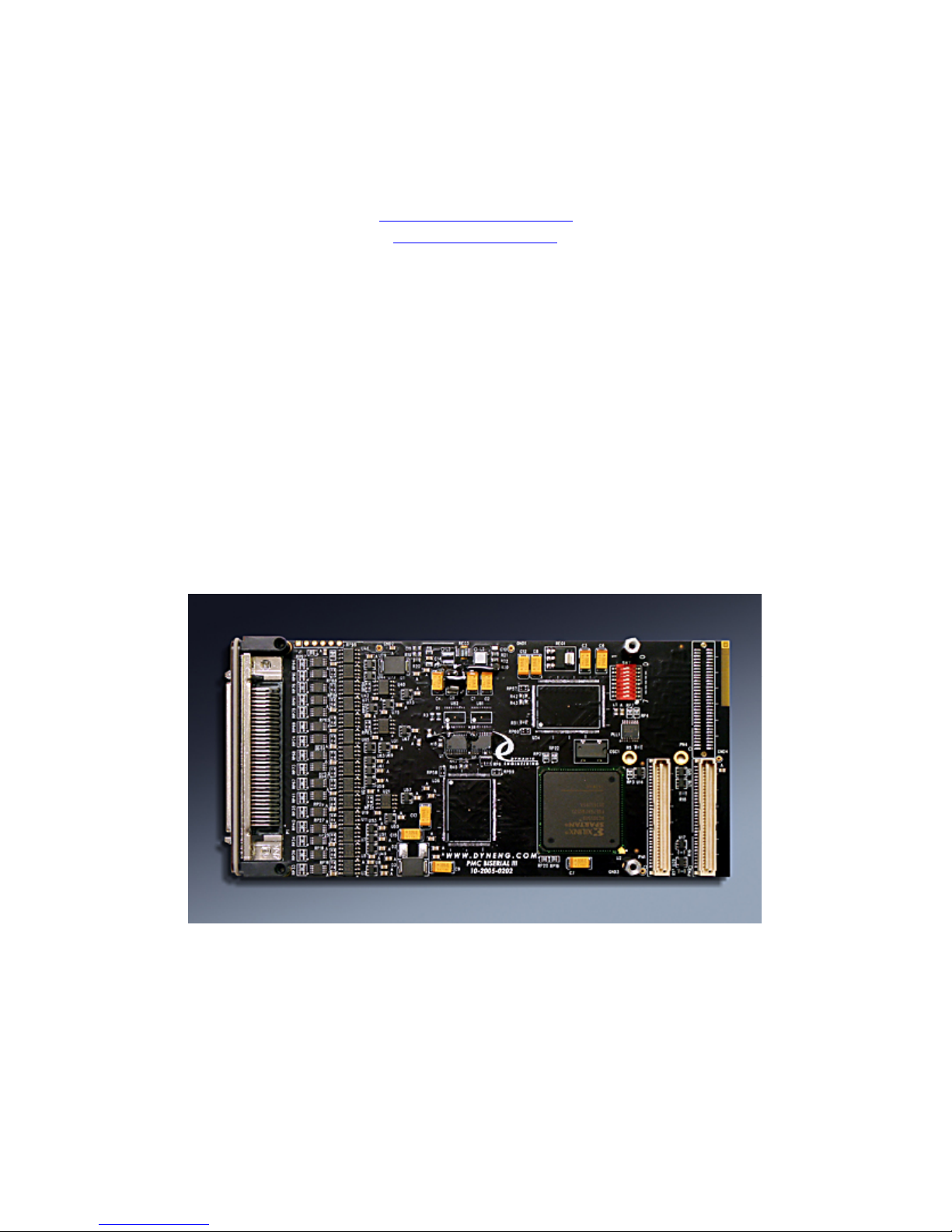
Product Description
The PMC-BiSerial-III RL1 is a part of the PMC Module family of modular I/O products by
Dynamic Engineering. It meets the PMC and CMC draft Standards. In standard
configuration, the PMC-BiSerial-III RL1 is a Type 1 mechanical with only low profile
passive components on the back of the board, one slot wide, with 10 mm inter-board
height. Contact Dynamic Engineering for a copy of this specification. It is assumed that
the reader is at least casually familiar with this document and basic logic design.
FIGURE 1 PMC-BISERIAL-III BLOCK DIAGRAM
The PMC-BiSerial-III is capable of providing multiple serial protocols using either LVDS
or RS-485 I/O standards. The PMC-BiSerial-III standard configuration shown in Figure
1 has two optional data FIFOs that can be as large as 128k x 32-bits to accommodate
designs requiring a large amount of buffering. In most designs these FIFOs are not
installed and internal FIFOs implemented with the block RAM in the Xilinx FPGA are
used instead.
Page 7
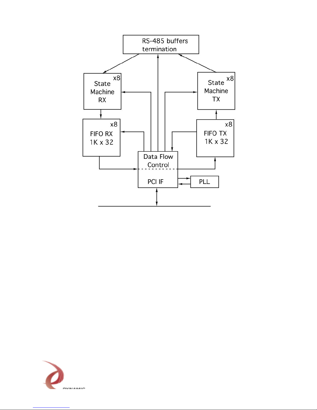
FIGURE 2 PMC-BISERIAL-III RL1 BLOCK DIAGRAM
The PMC-BiSerial-III RL1 configuration is shown in figure 2. The protocol implemented
provides eight I/O channels each consisting of RS-485 transmit and receive data. The
on-board PLL is used to generate two clocks that can be independently selected by
each channel in the design. The PLL is programmable and uses a 40 MHz reference
oscillator to generate a wide range of frequencies. The UART interface uses a 16x
clock to detect received data bits. The interface can operate at up to 10 Mbits/second
using a 160 MHz clock.
Data for all channels is sent and received LSB first using a low start-bit and one or two
high stop-bits to separate data bytes. An optional parity bit following the eight data bits
can be configured to implement odd, even, mark (always high), or space (always low)
parity. The marking (idle) state of the interface is high.
Each channel can be configured for either half or full-duplex operation. In half-duplex
mode, the receiver data is read from the transmit I/O while the transmitter is in a high
impedance state. Pull-up/pull-down resistor packs have been installed on the eight
transmit I/O lines to provide a logic ‘1’ when the I/O is un-driven. This prevents glitching
Page 8

when switching directions in half-duplex mode.
The RL1 implementation has two 1K by 32-bit FIFOs per channel, created using the
Xilinx internal block RAM, one for the transmitter and one for the receiver. The two
FIFOs have separate reset bits and a data bypass feature that automatically moves
data from the transmit to the receive FIFO to allow FIFO data-path testing without using
the external I/O.
Various interrupts are supported by the PMC-BiSerial-III RL1. An interrupt can be
configured to occur at the end of a received or transmitted message, when the transmit
FIFO becomes almost empty or when the receive FIFO becomes almost full or when
the receive FIFO overflows (attempt to write to a full FIFO). Receiver parity or framing
errors are detected and latched, but can not cause an interrupt to occur. All interrupts
are individually maskable, and a master channel interrupt enable is also provided to
disable all interrupts for a channel simultaneously. The current status is available even
when an interrupt is disabled making it possible to operate in a polled mode. All
configuration registers support read and write operations for maximum software
convenience. All addresses are long word (32-bit) aligned.
Potentially thirty-four differential I/O are available at the front bezel for the serial signals.
The drivers and receivers conform to the RS-485 specification. The RS-485 input
signals are selectively terminated with 100Ω. The termination resistors are in twoelement packages to allow flexible termination options for custom formats and
protocols. Optional pull-up/pull-down resistor packs can also be installed to provide a
logic ‘1’ on undriven lines. In this design 4.7 kΩ pull-up/pull-down resistors have been
installed on the eight transmit lines to prevent erroneous data when switching directions
in half-duplex mode. This design uses only sixteen of the I/O lines, one in and one out
for each of the eight channels.
Other custom interfaces are available on request. We will redesign the state machines
and create a custom interface protocol that meets your requirements. That protocol will
then be offered as a “standard” special order product. Please see our web page for
current protocols offered. Please contact Dynamic Engineering with your custom
application.
Since the PMC-BiSerial-III RL1 conforms to the PMC and CMC draft standards, it is
guaranteed to be compatibile with multiple PMC Carrier boards. Because the PMC may
be mounted on different form factors, while maintaining plug and software compatibility,
system prototyping may be done on one PMC Carrier board, while final system
implementation uses a different one.
The PMC-BiSerial-III RL1 uses a 10 mm inter-board spacing for the front panel,
standoffs, and PMC connectors. The 10 mm height is the "standard" height and will
work in most systems with most carriers. If your carrier has non-standard connectors
(height) to mate with the PMC-BiSerial-III RL1, please let us know. We may be able to
do a special build with a different height connector to compensate.
Page 9

Theory of Operation
The PMC-BiSerial-III RL1 features a Xilinx FPGA. The FPGA contains all of the
registers, FIFOs and protocol controlling elements of the PMC-BiSerial-III RL1 design.
Only the transceivers, switches and PLL circuit are external to the Xilinx device.
A logic block within the Xilinx controls the PCI interface to the host CPU. The PMCBiSerial-III RL1 design requires one wait state for read or writes cycles to any address.
The wait states refer to the number of clocks after the PCI core decodes the address
and control signals and before the “terminate with data” state is reached. Two
additional clock periods account for the delay to decode the signals from the PCI bus
and to convert the terminate-with-data state into the TRDY signal.
Scatter-gather DMA is provided for in this design with the memory page information
stored in host RAM as a series of chaining descriptors. Once the physical address of
the first chaining descriptor is written to the appropriate DMA pointer register, the
interface will read a 12-byte block from this location. The first four bytes comprise a
long-word indicating the physical address of the first block of the I/O buffer passed to
the read or write call. The next four bytes represent a long-word indicating the length of
that block. The final four bytes are a long-word indicating the physical address of the
next chaining descriptor along with two flag bits, in bit position 0 and 1. Bit zero is set to
a ‘1’ if this descriptor is the last in the chain. Bit one is set to a ‘1’ if the I/O transfer is
from the PMC-BiSerial-III RL1 board to host memory, and a ‘0’ if the transfer is from
memory to the board. These bits are then replaced with zeros to determine the address
of the next descriptor, if there is one.
To transmit data requires a number of steps to be performed. First, the PLL must be
programmed to supply the transmit clock. The data to be sent written to the TX FIFO
and the transmitter enabled. These steps do not need to be performed in this order, but
they must all be done to accomplish the transfer. If the requested transmit byte count is
zero, all the data written to the transmit FIFO will be sent, otherwise only the specified
number of bytes will be sent. The least significant byte of the FIFO word is sent first
then the next significant byte follows until the entire 32-bit word is sent. If a byte count
is requested that is not divisible by four, the remaining bytes of the last FIFO word are
discarded and a subsequent transmission will begin with the next FIFO word.
In order to receive data it is only necessary to configure the PLL, enable the receiver
and wait for data to be received. A 16-bit counter is incremented for each data byte
received. Once the reception has started, a 32-bit data word will be stored in the
receive FIFO for each four bytes received. The first byte is stored in the least significant
byte of the FIFO word and each subsequent byte is stored in the next most significant
byte. When the input data line is idle for at least eight bit-periods the reception will
terminate. This will cause the received byte count to be written to the byte count
register, clear the 16-bit byte counter and set the Receive Done status bit. If the last
FIFO word has not been completed, the last partial word will be written to the receive
Page 10

FIFO with the unfilled bytes set to zeros. Also if the Receive Start Clear Enable is set,
the Receiver Enable bit will be cleared. Otherwise the receiver will remain enabled and
will wait for the next start-bit to continue receiving data.
TX FIFO almost empty and RX FIFO almost full levels are programmable by writing
values into the respective FIFO level registers. Besides generating FIFO level status
and potentially causing an interrupt, these values can also be used to give DMA
arbitration priority to a FIFO approaching its limit if enabled to do so. This process helps
to prevent TX FIFO underrun and RX FIFO overrun when data is being transferred on
multiple channels. If a channel FIFO has reached its almost empty/full level, that FIFO
will get priority in the DMA arbiter if priority arbitration is enabled for that FIFO.
Page 11

Programming
Programming the PMC-BiSerial-III RL1 requires only the ability to read and write data
from the host. The base address is determined during system configuration of the PCI
bus. The base address refers to the first user address for the slot in which the PMC is
installed.
Depending on the software environment it may be necessary to set-up the system
software with the PMC-BiSerial-III RL1 "registration" data. For example in WindowsNT
there is a system registry, which is used to identify the resident hardware.
Before I/O data can be sent or received, the PLL must be programmed to the desired
clock configuration. The PLL is connected to the Xilinx by an I2C serial bus. The PLL
internal registers are loaded with 40 bytes of data that are derived from a .jed file
generated by the CyberClock utility from Cypress semiconductor
http://www.dyneng.com/CyberClocks.zip. Routines to program the PLL are included in
the driver and UserApp code provided in the engineering kit for the board.
The interrupt service routine should be loaded and the interrupt mask set. The interrupt
service routine can be configured to respond to the TX/RX interrupts. After an interrupt
is received, new TX data can be written or RX data retrieved. An efficient loop can then
be implemented to process the data. New messages can be sent or received even as
the current one is in progress.
If more than one interrupt is enabled, then the software needs to read the status to see
which source caused the interrupt. The status bits are latched, and are explicitly
cleared by writing a one to the corresponding bit. It is a good idea to read the status
register and write that value back to clear all the latched interrupt status bits before
starting a transfer. This will insure that the interrupt status values read by the interrupt
service routine came from the current transfer.
If DMA is to be used it will be necessary to acquire blocks of non-paged memory that
are accessible from the PCI bus in which to store the DMA chaining descriptor list
entries.
Refer to the Theory of Operation section above and the register definition section below
for more information regarding the exact sequencing and interrupt definitions.
The PMC-BiSerial-III RL1 VendorId = 0x10EE. The CardId = 0x0032. The device class
code is 0x0680 (PCI bridge – other)
Page 12

Address Map
Register Name Offset Description
RL1_BASE_CONTROL 0x0000 Base Control Register
RL1_PLL_WRITE 0x0000 Base Control - Bits 16-19 Used for PLL Control
RL1_PLL_READ 0x0004 Switch Port Bit 19 Used for pll_sdat Input
RL1_USER_SWITCH 0x0004 User Switch Read Port and Xilinx Design Revision
RL1_CHAN_0_CONTROL 0x0010 Channel 0 Control Register
RL1_CHAN_0_STATUS 0x0014 Channel 0 Status Register
RL1_CHAN_0_WR_DMA_PNTR 0x0018 Channel 0 Write DMA Physical PCI dpr Address
RL1_CHAN_0_TX_FIFO_COUNT 0x0018 Channel 0 TX FIFO Count
RL1_CHAN_0_RD_DMA_PNTR 0x001C Channel 0 Read DMA Physical PCI dpr Address
RL1_CHAN_0_RX_FIFO_COUNT 0x001C Channel 0 RX FIFO Count
RL1_CHAN_0_FIFO 0x0020 Channel 0 FIFO Single-Word Access
RL1_CHAN_0_TX_AMT_LVL 0x0024 Channel 0 TX almost empty level
RL1_CHAN_0_RX_AFL_LVL 0x0028 Channel 0 RX Almost Full Level
RL1_CHAN_0_TX_CONTROL 0x002C Channel 0 TX Control Register
RL1_CHAN_0_RX_CONTROL 0x0030 Channel 0 RX Control Register
RL1_CHAN_0_TX_START 0x0034 Channel 0 TX Start Latch
RL1_CHAN_0_RX_START 0x0038 Channel 0 RX Start Latch
RL1_CHAN_0_RX_BYTE_COUNT 0x0038 Channel 0 RX Byte Count
RL1_CHAN_1_CONTROL 0x003C Channel 1 Control Register
RL1_CHAN_1_STATUS 0x0040 Channel 1 Status Register
RL1_CHAN_1_WR_DMA_PNTR 0x0044 Channel 1 Write DMA Physical PCI dpr Address
RL1_CHAN_1_TX_FIFO_COUNT 0x0044 Channel 1 TX FIFO Count
RL1_CHAN_1_RD_DMA_PNTR 0x0048 Channel 1 Read DMA Physical PCI dpr Address
RL1_CHAN_1_RX_FIFO_COUNT 0x0048 Channel 1 RX FIFO Count
RL1_CHAN_1_FIFO 0x004C Channel 1 FIFO Single-Word Access
RL1_CHAN_1_TX_AMT_LVL 0x0050 Channel 1 TX almost empty level
RL1_CHAN_1_RX_AFL_LVL 0x0054 Channel 1 RX Almost Full Level
RL1_CHAN_1_TX_CONTROL 0x0058 Channel 1 TX Control Register
RL1_CHAN_1_RX_CONTROL 0x005C Channel 1 RX Control Register
RL1_CHAN_1_TX_START 0x0060 Channel 1 TX Start Latch
RL1_CHAN_1_RX_START 0x0064 Channel 1 RX Start Latch
RL1_CHAN_1_RX_BYTE_COUNT 0x0064 Channel 1 RX Byte Count
RL1_CHAN_2_CONTROL 0x0068 Channel 2 Control Register
RL1_CHAN_2_STATUS 0x006C Channel 2 Status Register
RL1_CHAN_2_WR_DMA_PNTR 0x0070 Channel 2 Write DMA Physical PCI dpr Address
RL1_CHAN_2_TX_FIFO_COUNT 0x0070 Channel 2 TX FIFO Count
RL1_CHAN_2_RD_DMA_PNTR 0x0074 Channel 2 Read DMA Physical PCI dpr Address
RL1_CHAN_2_RX_FIFO_COUNT 0x0074 Channel 2 RX FIFO Count
RL1_CHAN_2_FIFO 0x0078 Channel 2 FIFO Single-Word Access
RL1_CHAN_2_TX_AMT_LVL 0x007C Channel 2 TX almost empty level
RL1_CHAN_2_RX_AFL_LVL 0x0080 Channel 2 RX Almost Full Level
RL1_CHAN_2_TX_CONTROL 0x0084 Channel 2 TX Control Register
RL1_CHAN_2_RX_CONTROL 0x0088 Channel 2 RX Control Register
RL1_CHAN_2_TX_START 0x008C Channel 2 TX Start Latch
RL1_CHAN_2_RX_START 0x0090 Channel 2 RX Start Latch
RL1_CHAN_2_RX_BYTE_COUNT 0x0090 Channel 2 RX Byte Count
RL1_CHAN_3_CONTROL 0x0094 Channel 3 Control Register
RL1_CHAN_3_STATUS 0x0098 Channel 3 Status Register
RL1_CHAN_3_WR_DMA_PNTR 0x009C Channel 3 Write DMA Physical PCI dpr Address
RL1_CHAN_3_TX_FIFO_COUNT 0x009C Channel 3 TX FIFO Count
RL1_CHAN_3_RD_DMA_PNTR 0x00A0 Channel 3 Read DMA Physical PCI dpr Address
RL1_CHAN_3_RX_FIFO_COUNT 0x00A0 Channel 3 RX FIFO Count
RL1_CHAN_3_FIFO 0x00A4 Channel 3 FIFO Single-Word Access
RL1_CHAN_3_TX_AMT_LVL 0x00A8 Channel 3 TX almost empty level
RL1_CHAN_3_RX_AFL_LVL 0x00AC Channel 3 RX Almost Full Level
RL1_CHAN_3_TX_CONTROL 0x00B0 Channel 3 TX Control Register
RL1_CHAN_3_RX_CONTROL 0x00B4 Channel 3 RX Control Register
RL1_CHAN_3_TX_START 0x00B8 Channel 3 TX Start Latch
RL1_CHAN_3_RX_START 0x00BC Channel 3 RX Start Latch
RL1_CHAN_3_RX_BYTE_COUNT 0x00BC Channel 3 RX Byte Count
RL1_CHAN_4_CONTROL 0x00C0 Channel 4 Control Register
Page 13

RL1_CHAN_4_STATUS 0x00C4 Channel 4 Status Register
RL1_CHAN_4_WR_DMA_PNTR 0x00C8 Channel 4 Write DMA Physical PCI dpr Address
RL1_CHAN_4_TX_FIFO_COUNT 0x00C8 Channel 4 TX FIFO Count
RL1_CHAN_4_RD_DMA_PNTR 0x00CC Channel 4 Read DMA Physical PCI dpr Address
RL1_CHAN_4_RX_FIFO_COUNT 0x00CC Channel 4 RX FIFO Count
RL1_CHAN_4_FIFO 0x00D0 Channel 4 FIFO Single-Word Access
RL1_CHAN_4_TX_AMT_LVL 0x00D4 Channel 4 TX almost empty level
RL1_CHAN_4_RX_AFL_LVL 0x00D8 Channel 4 RX Almost Full Level
RL1_CHAN_4_TX_CONTROL 0x00DC Channel 4 TX Control Register
RL1_CHAN_4_RX_CONTROL 0x00E0 Channel 4 RX Control Register
RL1_CHAN_4_TX_START 0x00E4 Channel 4 TX Start Latch
RL1_CHAN_4_RX_START 0x00E8 Channel 4 RX Start Latch
RL1_CHAN_4_RX_BYTE_COUNT 0x00E8 Channel 4 RX Byte Count
RL1_CHAN_5_CONTROL 0x00EC Channel 5 Control Register
RL1_CHAN_5_STATUS 0x00F0 Channel 5 Status Register
RL1_CHAN_5_WR_DMA_PNTR 0x00F4 Channel 5 Write DMA Physical PCI dpr Address
RL1_CHAN_5_TX_FIFO_COUNT 0x00F4 Channel 5 TX FIFO Count
RL1_CHAN_5_RD_DMA_PNTR 0x00F8 Channel 5 Read DMA Physical PCI dpr Address
RL1_CHAN_5_RX_FIFO_COUNT 0x00F8 Channel 5 RX FIFO Count
RL1_CHAN_5_FIFO 0x00FC Channel 5 FIFO Single-Word Access
RL1_CHAN_5_TX_AMT_LVL 0x0100 Channel 5 TX almost empty level
RL1_CHAN_5_RX_AFL_LVL 0x0104 Channel 5 RX Almost Full Level
RL1_CHAN_5_TX_CONTROL 0x0108 Channel 5 TX Control Register
RL1_CHAN_5_RX_CONTROL 0x010C Channel 5 RX Control Register
RL1_CHAN_5_TX_START 0x0110 Channel 5 TX Start Latch
RL1_CHAN_5_RX_START 0x0114 Channel 5 RX Start Latch
RL1_CHAN_5_RX_BYTE_COUNT 0x0114 Channel 5 RX Byte Count
RL1_CHAN_6_CONTROL 0x0118 Channel 6 Control Register
RL1_CHAN_6_STATUS 0x011C Channel 6 Status Register
RL1_CHAN_6_WR_DMA_PNTR 0x0120 Channel 6 Write DMA Physical PCI dpr Address
RL1_CHAN_6_TX_FIFO_COUNT 0x0120 Channel 6 TX FIFO Count
RL1_CHAN_6_RD_DMA_PNTR 0x0124 Channel 6 Read DMA Physical PCI dpr Address
RL1_CHAN_6_RX_FIFO_COUNT 0x0124 Channel 6 RX FIFO Count
RL1_CHAN_6_FIFO 0x0128 Channel 6 FIFO Single-Word Access
RL1_CHAN_6_TX_AMT_LVL 0x012C Channel 6 TX almost empty level
RL1_CHAN_6_RX_AFL_LVL 0x0130 Channel 6 RX Almost Full Level
RL1_CHAN_6_TX_CONTROL 0x0134 Channel 6 TX Control Register
RL1_CHAN_6_RX_CONTROL 0x0138 Channel 6 RX Control Register
RL1_CHAN_6_TX_START 0x013C Channel 6 TX Start Latch
RL1_CHAN_6_RX_START 0x0140 Channel 6 RX Start Latch
RL1_CHAN_6_RX_BYTE_COUNT 0x0140 Channel 6 RX Byte Count
RL1_CHAN_7_CONTROL 0x0144 Channel 7 Control Register
RL1_CHAN_7_STATUS 0x0148 Channel 7 Status Register
RL1_CHAN_7_WR_DMA_PNTR 0x004C Channel 7 Write DMA Physical PCI dpr Address
RL1_CHAN_7_TX_FIFO_COUNT 0x004C Channel 7 TX FIFO Count
RL1_CHAN_7_RD_DMA_PNTR 0x0150 Channel 7 Read DMA Physical PCI dpr Address
RL1_CHAN_7_RX_FIFO_COUNT 0x0150 Channel 7 RX FIFO Count
RL1_CHAN_7_FIFO 0x0154 Channel 7 FIFO Single-Word Access
RL1_CHAN_7_TX_AMT_LVL 0x0158 Channel 7 TX almost empty level
RL1_CHAN_7_RX_AFL_LVL 0x015C Channel 7 RX Almost Full Level
RL1_CHAN_7_TX_CONTROL 0x0160 Channel 7 TX Control Register
RL1_CHAN_7_RX_CONTROL 0x0164 Channel 7 RX Control Register
RL1_CHAN_7_TX_START 0x0168 Channel 7 TX Start Latch
RL1_CHAN_7_RX_START 0x016C Channel 7 RX Start Latch
RL1_CHAN_7_RX_BYTE_COUNT 0x016C Channel 7 RX Byte Count
FIGURE 3 PMC-BISERIAL-III RL1 XILINX ADDRESS MAP
Page 14

Register Definitions
RL1_BASE_CONTROL
[0x0000] Base Control Register (read/write)
Base Control Register
Data Bit Description
31-20 Spare
19 PLL Sdata Output
18 PLL S2 Output
17 PLL Sclk Output
16 PLL Enable
15-0 Spare
FIGURE 4 PMC-BISERIAL-III RL1 BASE CONTROL REGISTER
All bits are active high and are reset on power-up or reset command, except PLL
enable, which defaults to enabled (high) on power-up or reset.
PLL Enable: When this bit is set to a one, the signals used to program and read the PLL
are enabled.
PLL Sclk/Sdata Output: These signals are used to program the PLL over the I2C serial
interface. Sclk is always an output whereas Sdata is bi-directional. This register is
where the Sdata output value is specified. When Sdata is an input it is read from the
User Switch Port.
PLL S2 Output: This is an additional control line to the PLL that can be used to select
additional pre-programmed frequencies.
Page 15

RL1_USER_SWITCH
[0x0004] User Switch Port (read only)
Dip-Switch Port
Data Bit Description
31-20 Spare
19 PLL Sdata Input
18-16 Spare
15-8 Xilinx Design Revision Number
7-0 Switch Setting
FIGURE 5 PMC-BISERIAL-III RL1 USER SWITCH PORT
Switch Setting: The user switch is read through this port. The bits are read as the
lowest byte in the port. Access the read-only port as a long word and mask off the
undefined bits. The dip-switch positions are defined in the silkscreen. For example the
switch figure below indicates a 0x12.
Xilinx Design Revision Number: The value of the second byte of this port is the rev.
number of the Xilinx design (currently 0x01 - rev. A.)
PLL Sdata Input: The PLL_sdata bi-directional line is read using this bit. This line is
used to read the register contents of the PLL.
1
7 0
0
Page 16

RL1_CHAN_0-7_CONTROL
[0x0010, 3C, 68, 94, C0, EC, 118, 144] Channel Control Register (read/write)
Channel Control Register
Data Bit Description
31-17 Spare
16 Divided Clock Select
15-12 Clock Divisor
11 PLL Clock A Select
10 Auto Direction Switch Enable
9 Full-Duplex Enable
8 Receive DMA Priority Arbitration Enable
7 Transmit DMA Priority Arbitration Enable
6 Read DMA Interrupt Enable
5 Write DMA Interrupt Enable
4 Force Interrupt
3 Master Interrupt Enable
2 FIFO Bypass Enable
1 Receive FIFO Reset
0 Transmit FIFO Reset
FIGURE 6 PMC-BISERIAL-III RL1 CHANNEL CONTROL REGISTER
Transmit/Receive FIFO Reset: When these bits are set to a one, the transmit and/or
receive FIFOs will be reset. When these bits are zero, normal FIFO operation is
enabled.
FIFO Bypass Enable: When this bit is set to a one, any data written to the transmit FIFO
will be immediately transferred to the receive FIFO. This allows for fully testing the data
FIFOs without using the I/O. When this bit is zero, normal FIFO operation is enabled.
Master Interrupt Enable: When this bit is set to a one, all enabled interrupts (except the
DMA interrupts) will be gated through to the PCI host; when this bit is a zero, the
interrupts can be used for status without interrupting the host.
Force Interrupt: When this bit is set to a one, a system interrupt will occur provided the
master interrupt enable is set. This is useful for interrupt testing.
Write/Read DMA Interrupt Enable: These two bits, when set to one, enable the
interrupts for DMA writes and reads respectively. The DMA interrupts are not affected
by the Master Interrupt Enable.
Page 17

Transmit / Receive DMA Priority Arbitration Enable: When this bit is set to a one, the
corresponding DMA channel will get priority if it is near the limit of its FIFO (almost
empty for the TX or almost full for the RX). These limits are derived from the
programmable counts in the RL1_CHAN_0-7_TX_AMT_LVL and RL1_CHAN_07_RX_AFL_LVL registers.
Full-Duplex Enable: When this bit is set to a one, the respective channel I/O will operate
in full-duplex mode. This means the transmit and receive data are transferred on
separate I/O lines and these transfers can occur simultaneously. When this bit is zero,
the I/O will operate in half-duplex mode. This means the transmit and receive data are
transferred on the same I/O line (the full-duplex transmit I/O line) and the transfers
cannot occur at the same time.
Auto Direction Switch Enable: When this bit is set to a one, and the channel I/O is
operating in half-duplex mode, the I/O interface will automatically change directions
when the current message completes provided transmit and receive interfaces are both
enabled. When this bit is zero, the I/O interface will not switch directions unless
explicitly commanded to do so.
PLL Clock A Select: When this bit is set to a one, the PLL clock A is selected for the I/O
reference clock. When this bit is zero, the PLL clock B is selected for the I/O reference
clock.
Clock Divisor: This field determines the reference clock divisor. The formula for
determining the divisor is 2 * (n + 1) where n is the value of this 4-bit field e.g. if n = 0
the divisor equals 2, if n = 1 the divisor equals 4, … if n = 15 the divisor equals 32.
Divided Clock Select: When this bit is set to a one, the divided clock is selected as the
16x reference clock for the channel I/O. When this bit is zero, the undivided PLL clock
is selected.
Page 18

RL1_CHAN_0-7_STATUS
[0x0014, 40, 6C, 98, C4, F0, 11C, 148] Channel Status Read/Clear Latch Write Port
Channel Status Register
Data Bit Description
31 Channel Interrupt Active
30-20 Spare
19 User Interrupt Condition Occurred
18 Receive FIFO Overflow Occurred
17 Receive Framing Error Occurred
16 Receive Parity Error Occurred
15 Read DMA Interrupt Occurred
14 Write DMA Interrupt Occurred
13 Read DMA Error Occurred
12 Write DMA Error Occurred
11 RX FIFO Almost Full Interrupt Occurred
10 TX FIFO Almost Empty Interrupt Occurred
9 Receive Done Interrupt Occurred
8 Transmit Done Interrupt Occurred
7 Receive Data Valid
6 Receive FIFO Full
5 Receive FIFO Almost Full
4 Receive FIFO Empty
3 Transmit Data Valid
2 Transmit FIFO Full
1 Transmit FIFO Almost Empty
0 Transmit FIFO Empty
FIGURE 7 PMC-BISERIAL-III RL1 CHANNEL STATUS PORT
Transmit FIFO Empty: When a one is read, the transmit data FIFO contains no data;
when a zero is read, there is at least one data word in the FIFO.
Transmit FIFO Almost Empty: When a one is read, the number of data words in the
transmit data FIFO is less than or equal to the value written to the
RL1_CHAN_TX_AMT_LVL register; when a zero is read, the FIFO level is more than
that value.
Transmit FIFO Full: When a one is read, the transmit data FIFO is full; when a zero is
read, there is room for at least one more data word in the FIFO.
Transmit Data Valid: When a one is read, there is a valid transmit data word in the
transmit holding register. This register is only loaded when the TX I/O is enabled and
transmit FIFO data has been loaded. This bit can be set even if the transmit FIFO is
Page 19

empty. When this bit is a zero, it indicates that there is no data in this holding register.
Receive FIFO Empty: When a one is read, the receive data FIFO contains no data;
when a zero is read, there is at least one data word in the FIFO.
Receive FIFO Almost Full: When a one is read, the number of data words in the receive
data FIFO is greater or equal to the value written to the RL1_CHAN_RX_AFL_LVL
register; when a zero is read, the FIFO level is less than that value.
Receive FIFO Full: When a one is read, the receive data FIFO is full; when a zero is
read, there is room for at least one more data-word in the FIFO.
Receive Data Valid: When a one is read, there is at least one valid receive data word
left. This bit can be set even if the receive FIFO is empty, because as soon as the first
four words are written into the FIFO, they are read out to fill the receive data pipe-line to
be ready for a PCI read DMA or single word access. When this bit is a zero, it indicates
that there is no valid receive data remaining.
Transmit Done Interrupt Occurred: When a one is read, it indicates that the transmit
state-machine has completed a message. A zero indicates that a transmit message
has not been completed. This bit is latched and can be cleared by writing back to the
Status register with a one in this bit position.
Receive Done Interrupt Occurred: When a one is read, it indicates that the receive
state-machine has received at least one complete message. At least one byte must
have been received and then the receive data line must be idle for at least eight bitperiods for a message be considered completed. A zero indicates that a complete
message has not been received. This bit is latched and can be cleared by writing back
to the Status register with a one in this bit position.
TX FIFO Almost Empty Interrupt Occurred: When a one is read, it indicates that the TX
FIFO was not almost empty and then the FIFO data count became less than or equal to
the value in the RL1_CHAN_TX_AMT_LVL register. A zero indicates that the FIFO has
not become almost empty. This bit is latched and can be cleared by writing back to the
Status register with a one in this bit position.
RX FIFO Almost Full Interrupt Occurred: When a one is read, it indicates that the RX
FIFO data count has become greater than or equal to the value in the
RL1_CHAN_RX_AFL_LVL register. A zero indicates that the FIFO has not become
almost full. This bit is latched and can be cleared by writing back to the Status register
with a one in this bit position.
Write/Read DMA Error Occurred: When a one is read, a write or read DMA error has
been detected. This will occur if there is a target or master abort or if the direction bit in
the next pointer of one of the chaining descriptors is incorrect. A zero indicates that no
write or read DMA error has occurred. These bits are latched and can be cleared by
Page 20

writing back to the Status register with a one in the appropriate bit position.
Write/Read DMA Interrupt Occurred: When a one is read, a write/read DMA interrupt is
latched. This indicates that the scatter-gather list for the current write or read DMA has
completed, but the associated interrupt has yet to be processed. A zero indicates that
no write or read DMA interrupt is pending.
Receive Parity Error Occurred: When a one is read, it indicates that a parity error was
detected in a received data-byte. A zero indicates that no parity error has occurred.
This bit is latched and can be cleared by writing back to the Status register with a one in
this bit position.
Receive Framing Error Occurred: When a one is read, it indicates that a framing error
has been detected in the receive data stream. This is caused by an incorrect stop bit.
A zero indicates that no framing error has occurred. This bit is latched and can be
cleared by writing back to the Status register with a one in this bit position.
Receive FIFO Overflow Occurred: When a one is read, it indicates that an attempt has
been made to write data to a full receive data FIFO. A zero indicates that no overflow
condition has occurred. This bit is latched and can be cleared by writing back to the
Status register with a one in this bit position.
User Interrupt Condition Occurred: When a one is read, it indicates that an enabled user
interrupt condition has occurred. These conditions include the TX and RX statemachine and FIFO interrupts as well as the RX FIFO overflow interrupt. Also the Force
Interrupt bit will cause this bit to be asserted. A system interrupt will occur if the Master
Interrupt Enable is set. A zero indicates that no enabled user interrupt condition is
active.
Channel Interrupt Active: When a one is read, it indicates that a system interrupt is
asserted caused by an enabled channel interrupt condition. A zero indicates that no
system interrupt is pending from an enabled channel interrupt condition
Page 21

RL1_CHAN_0-7_WR_DMA_PNTR
[0x0018, 44, 70, 9C, C8, F4, 120, 14C] Write DMA Pointer (write only)
DMA Pointer Address Register
Data Bit Description
31-0 First Chaining Descriptor Physical Address
FIGURE 8 PMC-BISERIAL-III RL1 WRITE DMA POINTER REGISTER
This write-only port is used to initiate a scatter-gather write DMA. When the address of
the first chaining descriptor is written to this port, the DMA engine reads three
successive long words beginning at that address. The first is the address of the first
memory block of the DMA buffer containing the data to write to the device, the second is
the length in bytes of that block, and the third is the address of the next chaining
descriptor in the list of buffer memory blocks. This process is continued until the end-ofchain bit in one of the next pointer values read indicates that it is the last chaining
descriptor in the list.
Note: Writing a zero to this port will abort a write DMA in progress.
RL1_CHAN_0-7_TX_FIFO_COUNT
[0x0018, 44, 70, 9C, C8, F4, 120, 14C] TX FIFO data count (read only)
TX FIFO Data Count Port
Data Bit Description
31-12 Spare
11-0 TX Data Words Stored
FIGURE 9 PMC-BISERIAL-III RL1 TX FIFO DATA COUNT PORT
This read-only register port reports the number of 32-bit data words in the transmit FIFO
and data holding register (currently a maximum of 0x401).
Page 22

RL1_CHAN_0-7_RD_DMA_PNTR
[0x001C, 48, 74, A0, CC, F8, 124, 150] Read DMA Pointer (write only)
DMA Pointer Address Register
Data Bit Description
31-0 First Chaining Descriptor Physical Address
FIGURE 10 PMC-BISERIAL-III RL1 READ DMA POINTER REGISTER
This write-only port is used to initiate a scatter-gather read DMA. When the address of
the first chaining descriptor is written to this port, the DMA engine reads three
successive long words beginning at that address. The first is the address of the first
memory block of the DMA buffer where the data from the device will be stored, the
second is the length in bytes of that block, and the third is the address of the next
chaining descriptor in the list of buffer memory blocks. This process is continued until
the end-of-chain bit in one of the next pointer values read indicates that it is the last
chaining descriptor in the list.
Note: Writing a zero to this port will abort a read DMA in progress.
RL1_CHAN_0-7_RX_FIFO_COUNT
[0x001C, 48, 74, A0, CC, F8, 124, 150] RX FIFO data count (read only)
RX FIFO Data Count Port
Data Bit Description
31-12 Spare
11-0 RX Data Words Stored
FIGURE 11 PMC-BISERIAL-III RL1 RX FIFO DATA COUNT PORT
This read-only register port reports the number of 32-bit data words in the receive FIFO
and data pipeline (currently a maximum of 0x404).
Page 23

RL1_CHAN_0-7_FIFO
[0x0020, 4C, 78, A4, D0, FC, 128, 154] Write TX/Read RX FIFO Port
RX and TX FIFO Port
Data Bit Description
31-0 FIFO data word
FIGURE 12 PMC-BISERIAL-III RL1 RX/TX FIFO PORT
This port is used to make single-word accesses into the TX and out of the RX FIFO.
RL1_CHAN_0-7_TX_AMT_LVL
[0x0024, 50, 7C, A8, D4, 100, 12C, 158] TX almost-empty level (read/write)
TX Almost-Empty Level Register
Data Bit Description
31-16 Spare
15-0 TX FIFO Almost-Empty Level
FIGURE 13 PMC-BISERIAL-III RL1 TX ALMOST EMPTY LEVEL REGISTER
This read/write port accesses the transmitter almost-empty level register. When the
number of data words in the transmit data FIFO is equal or less than this value, the
almost-empty status bit will be set.
RL1_CHAN_0-7_RX_AFL_LVL
[0x0028, 54, 80, AC, D8, 104, 130, 15C] RX almost-full level (read/write)
RX Almost-Full Level Register
Data Bit Description
31-16 Spare
15-0 RX FIFO Almost-Full Level
FIGURE 14 PMC-BISERIAL-III RL1 RX ALMOST FULL LEVEL REGISTER
This read/write port accesses the receiver almost-full level register. When the number
of data words in the receive data FIFO is equal or greater than this value, the almost-full
status bit will be set.
Page 24

RL1_CHAN_0-7_TX_CONTROL
[0x002C, 58, 84, B0, DC, 108, 134, 160] Channel Control Register (read/write)
Channel Control Register
Data Bit Description
31-8 Spare
7 Transmit Parity Level Select
6 Transmit Odd Parity Select
5 Transmit Parity Enable
4 Transmit Two Stop-Bits Select
3 Transmit Start Clear Enable
2 TX FIFO Almost Empty Interrupt Enable
1 Transmit Done Interrupt Enable
0 Transmitter Enabled (read only)
FIGURE 15 PMC-BISERIAL-III RL1 TX CONTROL REGISTER
Transmitter Enabled: When a one is read, the transmit state-machine is enabled and
either a message is in progress or it is waiting for data to be written to the transmit
FIFO; when a zero is read, the state-machine is disabled.
Transmitter Done Interrupt Enable: When this bit is a one the transmitter interrupt is
enabled. The interrupt will occur when the transmit state-machine completes a
message. If the requested byte count equals zero, this will occur when all the FIFO
data has been sent otherwise it will occur when the byte count request has been
satisfied. In either case, at least one byte must be sent to constitute a transmitted
message.
TX FIFO Almost Empty Interrupt Enable: When this bit is set to a one, the transmit FIFO
almost empty interrupt is enabled. An interrupt will be asserted when the FIFO level
becomes less than or equal to the count in the RL1_CHAN0-7_TX_AMT_LVL register,
provided the master interrupt enable is asserted. When this bit is zero, the transmit
FIFO almost empty interrupt is disabled.
Transmit Start Clear Enable: When this bit is set to a one, the TX start latch will be
cleared when the current transmit message completes. When this bit is zero, the TX
start latch will remain set until the transmitter is disabled.
Transmit Two Stop-Bits Select: When this bit is set to a one, the transmitter will insert
two stop-bits to terminate a data-byte. When this bit is zero, only one stop-bit will be
inserted
Transmit Parity Enable: When this bit is set to a one, a parity bit will be added after the
eight data-bits and before the stop-bit(s). When this bit is zero, no parity bit will be
Page 25

added.
Transmit Odd Parity Select: When this bit is set to a one, odd parity will be used to
determine the polarity of the parity bit, provided the Parity Level Select bit is a zero.
When this bit is zero, even parity will be used.
Transmit Parity Level Select: When this bit is set to a one, the parity bit will be equal to
the value of the Odd Parity Select bit. When this bit is zero, the polarity of the parity bit
will be calculated using odd or even parity as determined by the Odd Parity Select bit.
RL1_CHAN_0-7_RX_CONTROL
[0x0030, 5C, 88, B4, E0, 10C, 138, 164] Channel Control Register (read/write)
Channel Control Register
Data Bit Description
31-10 Spare
9 Receive Parity Level Select
8 Receive Odd Parity Select
7 Receive Parity Enable
6 Receive Two Stop-Bits Select
5 Receiver Termination Enable
4 Receive Start Clear Enable
3 RX FIFO Overflow Interrupt Enable
2 RX FIFO Almost Full Interrupt Enable
1 Receive Done Interrupt Enable
0 Receiver Enabled (read only)
FIGURE 16 PMC-BISERIAL-III RL1 RX CONTROL REGISTER
Receiver Enabled: When a one is read, the Receive state-machine is enabled and
either a message is in progress or it is waiting for a message to begin; when a zero is
read, the state-machine is disabled.
Receiver Done Interrupt Enable: When this bit is a one the Receiver interrupt is
enabled. The interrupt will occur when the Receive state-machine receives a complete
message. This will occur when the at least one byte has been received and then the
receive data line is idle for at least eight bit-periods.
RX FIFO Almost Full Interrupt Enable: When this bit is set to a one, the receive FIFO
almost full interrupt is enabled. An interrupt will be asserted when the FIFO level
becomes greater than or equal to the count in the RL1_CHAN0-7_RX_AFL_LVL
register, provided the master interrupt enable is asserted. When this bit is zero, the RX
FIFO almost full interrupt is disabled.
Page 26

Receive FIFO Overflow Interrupt Enable: When this bit is set to a one, the receive FIFO
overflow interrupt is enabled. An interrupt will be asserted, provided the master
interrupt is enabled when an attempt is made to write to a full receive FIFO. When this
bit is zero, the receive FIFO overflow interrupt is disabled.
Receive Start Clear Enable: When this bit is set to a one, the RX start latch will be
cleared when the current Receive message completes. When this bit is zero, the RX
start latch will remain set until the Receiver is disabled.
Receiver Termination Enable: When this bit is set to a one, the 100 Ω receiver I/O shunt
termination is enabled when the I/O line is operating in full-duplex mode or in halfduplex mode with the transmitter disabled. This termination is used to reduce noise on
the I/O line. If more than one receiver is being driven by the same source, be careful
not to enable more than one termination as this could excessively attenuate the signal.
When this bit is zero, the termination is disabled.
Receive Two Stop-Bits Select: When this bit is set to a one, the Receiver will expect two
stop-bits to terminate a data-byte. When this bit is zero, only one stop-bit will be
expected. If the expected stop bits are not received as ones, a framing error will be
latched.
Receive Parity Enable: When this bit is set to a one, a parity bit will be expected after
the eight data-bits and before the stop-bit(s). When this bit is zero, no parity bit will be
expected. If parity is enabled and the parity bit does not match the calculated value, a
parity error will be latched.
Receive Odd Parity Select: When this bit is set to a one, odd parity will be used to
determine the polarity of the expected parity bit, provided the Parity Level Select bit is a
zero. When this bit is zero, even parity will be used.
Receive Parity Level Select: When this bit is set to a one, the expected parity bit will be
equal to the value of the Odd Parity Select bit. When this bit is zero, the polarity of the
expected parity bit will be calculated using odd or even parity as determined by the Odd
Parity Select bit.
Page 27

RL1_CHAN_0-7_TX_START_LATCH
[0x0034, 60, 8C, B8, E4, 110, 13C, 168] TX start (write only)
TX Start Latch
Data Bit Description
31-17 Spare
16-1 TX Byte Count
0 TX Start
FIGURE 17 PMC-BISERIAL-III RL1 TX START LATCH
TX Start: When this bit is set to a one, the transmit state-machine will be enabled.
When this bit is zero the state-machine will be disabled. The value of the TX start bit is
read from the TX_CONTROL register bit 0.
TX Byte Count: This 16-bit field determines the number of bytes to send when the
transmitter is enabled. If TX Byte Count is equal to zero, transmit data will be sent until
the TX FIFO data is exhausted.
RL1_CHAN_0-7_RX_START_LATCH
[0x0038, 64, 90, BC, E8, 114, 140, 16C] RX start (write only)
RX Start Latch
Data Bit Description
31-1 Spare
0 RX Start
FIGURE 18 PMC-BISERIAL-III RL1 RX START LATCH
RX Start: When this bit is set to a one, the receive state-machine will be enabled. When
this bit is zero the state-machine will be disabled. The value of the RX start bit is read
from the RX_CONTROL register bit 0.
Page 28

RL1_CHAN_0-7_RX_BYTE_COUNT
[0x0038, 64, 90, BC, E8, 114, 140, 16C] RX byte count (read only)
RX Byte Count Port
Data Bit Description
31-16 Spare
15-0 RX Bytes Received
FIGURE 19 PMC-BISERIAL-III RL1 RX BYTE COUNT PORT
RX Bytes Received: This field represents the number of bytes received in the last
message. The value will remain valid until the end of a subsequent message. The
Receive Done Interrupt can be used to indicate when this value has been updated.
Page 29

Loop-back
The Engineering kit has reference software, which includes external loop-back tests.
The PMC-BISERIAL-III RL1 has a 68 pin SCSI II front panel connector. The tests
require an external cable with the following pins connected.
Full-Duplex Loop-Back
Signal From To Signal
TX0 DATA+ pin 1 pin 2 RX0 DATA+
TX0 DATA- pin 35 pin 36 RX0 DATATX1 DATA+ pin 3 pin 4 RX1 DATA+
TX1 DATA- pin 37 pin 38 RX1 DATATX2 DATA+ pin 5 pin 6 RX2 DATA+
TX2 DATA - pin 39 pin 40 RX2 DATATX3 DATA+ pin 7 pin 8 RX3 DATA+
TX3 DATA- pin 41 pin 42 RX3 DATATX4 DATA+ pin 9 pin 10 RX4 DATA+
TX4 DATA- pin 43 pin 44 RX4 DATATX5 DATA+ pin 11 pin 12 RX5 DATA+
TX5 DATA- pin 45 pin 46 RX5 DATATX6 DATA+ pin 13 pin 14 RX6 DATA+
TX6 DATA - pin 47 pin 48 RX6 DATATX7 DATA+ pin 15 pin 16 RX7 DATA+
TX7 DATA- pin 49 pin 50 RX7 DATA-
Half-Duplex Loop-Back
Signal From To Signal
TX/RX 0 DATA+ pin 1 pin 3 TX/RX 1 DATA+
TX/RX 0 DATA- pin 35 pin 37 TX/RX 1 DATATX/RX 2 DATA+ pin 5 pin 7 TX/RX 3 DATA+
TX/RX 2 DATA - pin 39 pin 41 TX/RX 3 DATATX/RX 4 DATA+ pin 9 pin 11 TX/RX 5 DATA+
TX/RX 4 DATA- pin 43 pin 45 TX/RX 5 DATATX/RX 6 DATA+ pin 13 pin 15 TX/RX 7 DATA+
TX/RX 6 DATA - pin 47 pin 49 TX/RX 7 DATA-
Page 30

PMC PCI Pn1 Interface Pin Assignment
The figure below gives the pin assignments for the PMC Module PCI Pn1 Interface on
the PMC-BISERIAL-III RL1. See the User Manual for your carrier board for more
information. Unused pins may be assigned by the specification but not needed by this
design.
TCK -12V 1 2
GND INTA# 3 4
5 6
BUSMODE1# +5V 7 8
9 10
GND 11 12
CLK GND 13 14
GND 15 16
+5V 17 18
AD31 19 20
AD28 AD27 21 22
AD25 GND 23 24
GND C/BE3# 25 26
AD22 AD21 27 28
AD19 +5V 29 30
AD17 31 32
FRAME# GND 33 34
GND IRDY# 35 36
DEVSEL# +5V 37 38
GND LOCK# 39 40
41 42
PAR GND 43 44
AD15 45 46
AD12 AD11 47 48
AD9 +5V 49 50
GND C/BE0# 51 52
AD6 AD5 53 54
AD4 GND 55 56
AD3 57 58
AD2 AD1 59 60
+5V 61 62
GND 63 64
FIGURE 20 PMC-BISERIAL-III RL1 PN1 INTERFACE
Page 31

PMC PCI Pn2 Interface Pin Assignment
The figure below gives the pin assignments for the PMC Module PCI Pn2 Interface on
the PMC-BISERIAL-III RL1. See the User Manual for your carrier board for more
information. Unused pins may be assigned by the specification but not needed by this
design.
+12V 1 2
TMS TDO 3 4
TDI GND 5 6
GND 7 8
9 10
11 12
RST# BUSMODE3# 13 14
BUSMODE4# 15 16
GND 17 18
AD30 AD29 19 20
GND AD26 21 22
AD24 23 24
IDSEL AD23 25 26
AD20 27 28
AD18 29 30
AD16 C/BE2# 31 32
GND 33 34
TRDY# 35 36
GND STOP# 37 38
PERR# GND 39 40
SERR# 41 42
C/BE1# GND 43 44
AD14 AD13 45 46
GND AD10 47 48
AD8 49 50
AD7 51 52
53 54
GND 55 56
57 58
GND 59 60
61 62
GND 63 64
FIGURE 21 PMC-BISERIAL-III RL1 PN2 INTERFACE
Page 32

Front Panel I/O Pin Assignment
The figure below gives the pin assignments for the PMC Module I/O Interface on the
PMC-BiSerial-III RL1. For a customized version, or other options, contact Dynamic
Engineering.
IO_0p (TX0 DATA +) IO_0m (TX0 DATA -) 1 35
IO_1p (RX0 DATA +) IO_1m (RX0 DATA -) 2 36
IO_2p (TX1 DATA +) IO_2m (TX1 DATA -) 3 37
IO_3p (RX1 DATA +) IO_3m (RX1 DATA -) 4 38
IO_4p (TX2 DATA +) IO_4m (TX2 DATA -) 5 39
IO_5p (RX2 DATA +) IO_5m (RX2 DATA -) 6 40
IO_6p (TX3 DATA +) IO_6m (TX3 DATA -) 7 41
IO_7p (RX3 DATA +) IO_7m (RX3 DATA -) 8 42
IO_8p (TX4 DATA +) IO_8m (TX4 DATA -) 9 43
IO_9p (RX4 DATA +) IO_9m (RX4 DATA -) 10 44
IO_10p (TX5 DATA +) IO_10m (TX5 DATA -) 11 45
IO_11p (RX5 DATA +) IO_11m (RX5 DATA -) 12 46
IO_12p (TX6 DATA +) IO_12m (TX6 DATA -) 13 47
IO_13p (RX6 DATA +) IO_13m (RX6 DATA -) 14 48
IO_14p (TX7 DATA +) IO_14m (TX7 DATA -) 15 49
IO_15p (RX7 DATA +) IO_15m (RX7 DATA -) 16 50
IO_16p IO_16m 17 51
IO_17p IO_17m 18 52
IO_18p IO_18m 19 53
IO_19p IO_19m 20 54
IO_20p IO_20m 21 55
IO_21p IO_21m 22 56
IO_22p IO_22m 23 57
IO_23p IO_23m 24 58
IO_24p IO_24m 25 59
IO_25p IO_25m 26 60
IO_26p IO_26m 27 61
IO_27p IO_27m 28 62
IO_28p IO_28m 29 63
IO_29p IO_29m 30 64
IO_30p IO_30m 31 65
IO_31p IO_31m 32 66
IO_32p IO_32m 33 67
IO_33p IO_33m 34 68
FIGURE 22 PMC-BISERIAL-III RL1 FRONT PANEL INTERFACE
Page 33

Embedded Solutions Page 33 of 37
Applications Guide
Interfacing
Some general interfacing guidelines are presented below. Do not hesitate to contact
the factory if you need more assistance.
ESD
Proper ESD handling procedures must be followed when handling the PMC-BISERIALIII RL1. The card is shipped in an anti-static, shielded bag. The card should remain in
the bag until ready for use. When installing the card the installer must be properly
grounded and the hardware should be on an anti-static workstation.
Start-up
Make sure that the "system" can see your hardware before trying to access it. Many
BIOS will display the PCI devices found at boot up on a "splash screen" with the
VendorID and CardId and an interrupt level. Look quickly, if the information is not
available from the BIOS then a third party PCI device cataloging tool will be helpful. We
use PCIView.
Watch the system grounds
All electrically connected equipment should have a fail-safe common ground that is
large enough to handle all current loads without affecting noise immunity. Power
supplies and power consuming loads should all have their own ground wires back to a
common point.
We provide the components. You provide the system. Only careful planning and
practice can achieve safety and reliability. Inputs can be damaged by static discharge,
or by applying voltage outside of the device rated voltages.
Page 34

Embedded Solutions Page 34 of 37
Construction and Reliability
PMC Modules were conceived and engineered for rugged industrial environments. The
PMC-BISERIAL-III RL1 is constructed out of 0.062-inch thick FR4 material.
Through-hole and surface-mount components are used. The PMC connectors are rated
at 1 Amp per pin, 100 insertion cycles minimum. These connectors make consistent,
correct insertion easy and reliable.
The PMC is secured against the carrier with four screws attached to the 2 stand-offs
and 2 locations on the front panel. The four screws provide significant protection
against shock, vibration, and incomplete insertion.
The PMC Module provides a low temperature coefficient of 2.17 W/°C for uniform heat.
This is based upon the temperature coefficient of the base FR4 material of 0.31 W/m-
°C, and taking into account the thickness and area of the PMC. The coefficient means
that if 2.17 Watts are applied uniformly on the component side, then the temperature
difference between the component side and solder side is one degree Celsius.
Thermal Considerations
The PMC-BISERIAL-III RL1 design consists of CMOS circuits. The power dissipation
due to internal circuitry is very low. It is possible to create higher power dissipation with
the externally connected logic. If more than one Watt is required to be dissipated due to
external loading, then forced-air cooling is recommended. With the one degree
differential temperature to the solder side of the board, external cooling is easily
accomplished.
Warranty and Repair
Please refer to the warranty page on our website for the current warranty offered and
options.
http://www.dyneng.com/warranty.html
Page 35

Embedded Solutions Page 35 of 37
Service Policy
Before returning a product for repair, verify as well as possible that the suspected unit is
at fault. Then call the Customer Service Department for a RETURN MATERIAL
AUTHORIZATION (RMA) number. Carefully package the unit, in the original shipping
carton if this is available, and ship prepaid and insured with the RMA number clearly
written on the outside of the package. Include a return address and the telephone
number of a technical contact. For out-of-warranty repairs, a purchase order for repair
charges must accompany the return. Dynamic Engineering will not be responsible for
damages due to improper packaging of returned items. For service on Dynamic
Engineering Products not purchased directly from Dynamic Engineering contact your
reseller. Products returned to Dynamic Engineering for repair by other than the original
customer will be treated as out-of-warranty.
Out of Warranty Repairs
Out of warranty repairs will be billed on a material and labor basis. The current
minimum repair charge is $100. Customer approval will be obtained before repairing
any item if the repair charges will exceed one half of the quantity one list price for that
unit. Return transportation and insurance will be billed as part of the repair and is in
addition to the minimum charge.
For Service Contact:
Customer Service Department
Dynamic Engineering
150 DuBois, Suite C
Santa Cruz, CA 95060
(831) 457-8891 Fax (831) 457-4793
support@dyneng.com
Page 36

Embedded Solutions Page 36 of 37
Specifications
Host Interface: [PMC] PCI Mezzanine Card – 32-bit, 33 MHz
Serial Interfaces: Sixteen UART interfaces (one in and one out per channel). 8-bit
data, LSB first, one start-bit, one or two stop-bits and optional parity
TX Bit-rates generated: Up to 10 Mbits/second for TX and RX, clock references supplied by
the on-board PLL (clock A or B independently selectable),
independent divisors from 1 to 32 (even numbers only).
Software Interface: Control Registers, FIFOs, and Status Ports
Initialization: Hardware reset forces all registers to 0 except as noted
Access Modes: LW boundary Space (see memory map)
Wait States: One for all addresses
Interrupt: TX message sent, RX message received, TX FIFO almost empty,
RX FIFO almost full and RX FIFO overflow for each channel
DMA: 16-channel Scatter/Gather DMA support implemented
Onboard Options: All Options are Software Programmable
Interface Options: 68 pin twisted pair cable
68 screw terminal block interface
Dimensions: Standard Single PMC Module
Construction: High Temp ROHS compliant FR4 Multi-Layer Printed Circuit,
Through-Hole and Surface-Mount Components
Temperature Coefficient: 2.17 W/oC for uniform heat across PMC
Power: Max. TBD mA @ 5V
Temperature range Standard (0 to +70)
Extended Temperature available (-40 to +85)
Page 37

Embedded Solutions Page 37 of 37
Order Information
PMC-BISERIAL-III RL1 PMC Module with 8 serial channels, two RS-485 I/O
per channel (one in and one out). Bezel IO is
standard. Rear IO available by request.
Eng Kit PMC-BISERIAL-III RL1 HDEterm68 - 68 position screw terminal adapter
http://www.dyneng.com/HDEterm68.html
HDEcabl68 - 68 I/O twisted pair cable
http://www.dyneng.com/HDEcabl68.html
Technical Documentation,
1. PMC-BiSerial-III Schematic
2. PMC-BISERIAL-III RL1 Driver software and
user application.
Data sheet reprints are available from the
manufacturer’s web site
-ROHS Add for ROHS processing. Standard soldering and
parts used otherwise.
-ET Industrial Temperature option [-40 +85C parts
used]
-CC Conformal Coating option
Note: The Engineering Kit is strongly recommended for first time PMC-BiSerial-III
purchases.
Schematics
Schematics are provided as part of the engineering kit for customer reference only.
This information was current at the time the printed circuit board was last revised. The
revision letter is shown on the front of this manual as “Corresponding Hardware
Revision.” This information is not necessarily current or complete manufacturing data,
nor is it part of the product specification.
All information provided is Copyright Dynamic Engineering
 Loading...