

Page 1
DYNAMIC ENGI NEERING
150 DuBois, Suite 3 Santa Cruz, CA 95060
(831) 457-8891 Fax (831) 457-4793
www.dyneng.com
sales@dyneng.com
Est. 1988
User Manual
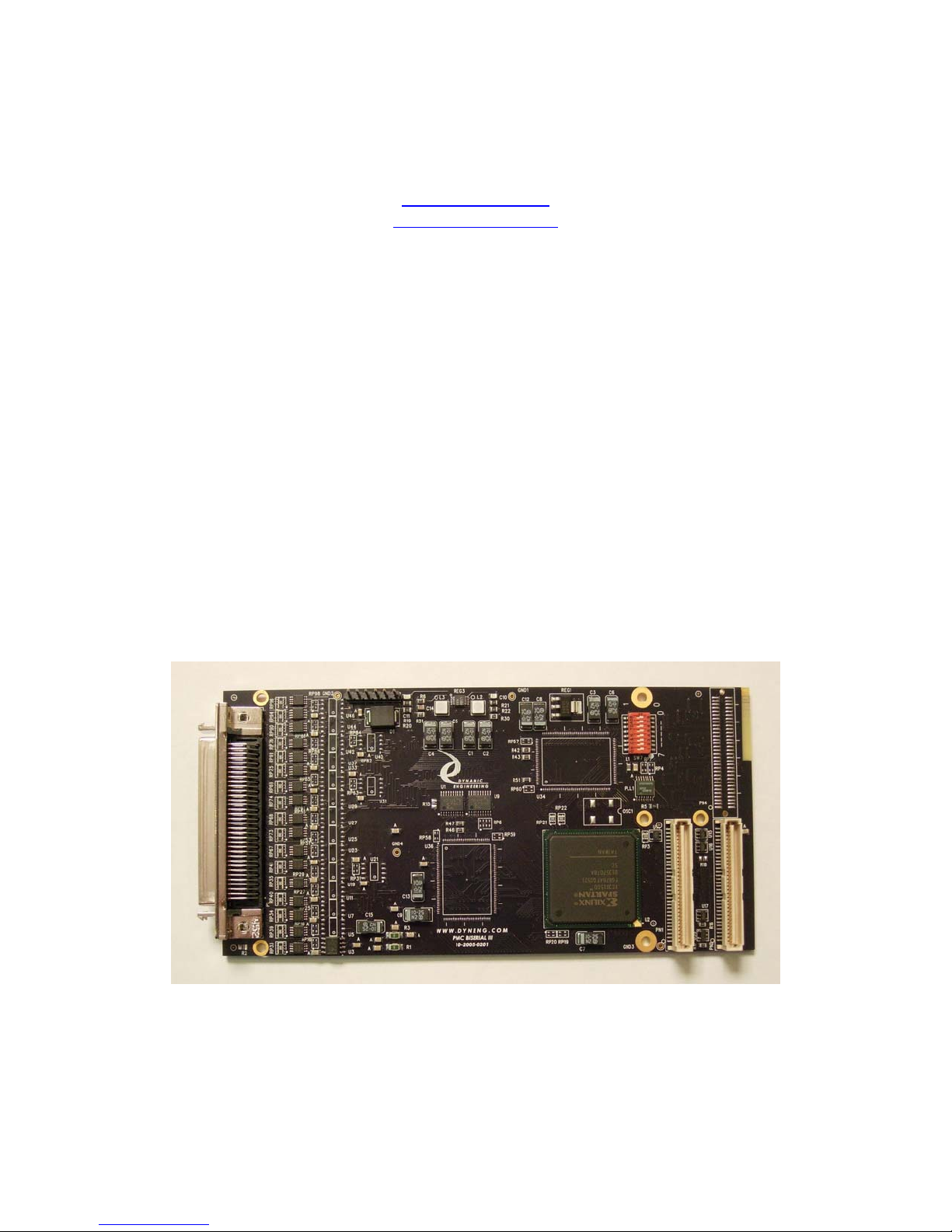
PMC-BiSerial-III HW2
32 channel
Bi-directional Manchester, SDLC and
Asynchronous Interface
PMC Module
Revision A
Corresponding Hardware: Revision C
10-2005-0503
Corresponding Firmware: Revision B
Page 2

y
y
g
PMC-BiSerial-III HW2
Bi-Directional Serial Data Interface
PMC Module
Dynamic Engineering
150 DuBois, Suite 3
Santa Cruz, CA 95060
(831) 457-8891
FAX: (831) 457-4793
©2005-2007 by Dynamic Engineering.
Other trademarks and registered trademarks are
owned by their respective manufactures.
Revised September 25, 2007.
This document contains information of
proprietary interest to Dynamic Engineering. It
has been supplied in confidence and the
recipient, by accepting this material, agrees that
the subject mat ter will not be copied or
reproduced, in whole or in part, nor its contents
revealed in any manner or to any person except
to meet the purpose for which it was delivered.
Dynamic Engineering has made every effort to
ensure that this manual is accurate and
complete. Still, the compan
reserves the right to
make improvements or changes in the product
described in this document at any time and
without notice. Furthermore, D
namic
Engineering assumes no liability arising out of
the application or use of the device described
herein.
The electronic equipment described herein
enerates, uses, and can radiate radio frequency
energy. Operation of this equipment in a
residential area is likely to cause radio
interference, in which case the user, at his own
expense, will be required to take whatever
measures may be required to correct the
interference.
Dynamic Engineering’s products are not
authorized for use as critical components in life
support devices or systems without the express
written approval of the president of Dynamic
Engineering.
This product has been designed to operate with
PMC Module carriers and compatible userprovided equipment. Connection of incompatible
hardware is likely to cause serious damage.
Embedded Solutions Page 2 of 50
Page 3

Table of Contents
PRODUCT DESCRIPTION 6
THEORY OF OPERATION 11
ADDRESS MAP 14
PROGRAMMING 16
REGISTER DEFINITIONS 17
BIS3_BASE 17
BIS3_ID 18
BIS3_START_SET 18
BIS3_START_RDBK 18
BIS3_START_CLR 19
BIS3_IO_DATA 20
BIS3_IO_DIR 20
BIS3_IO_TERM 21
BIS3_IO_MUX 21
BIS3_IO_UCNTL 22
BIS3_IO_RDBK 22
BIS3_IO_RDBKUPR 23
BIS3_STAT_FIFO 23
BIS3_PLL_CMD, PLL_RDBK 24
BIS3_SM_CNTL7-0 25
BIS3_SDLC_CNTL5-0 28
BIS3_ASYNC_CNTL11-0 30
BIS3_CHAN_MODE 32
BIS3_INT_STAT 33
BIS3_I2OAR 33
BIS3_SM_MEM31-0 34
Mode Resource Mapping 39
Interrupts 40
Loop-back 41
PMC PCI PN1 INTERFACE PIN ASSIGNMENT 42
PMC PCI PN2 INTERFACE PIN ASSIGNMENT 43
Embedded Solutions Page 3 of 50
Page 4

BISERIAL III FRONT PANEL I/O PIN ASSIGNMENT 44
APPLICATIONS GUIDE 45
Interfacing 45
CONSTRUCTION A ND RELIABILITY 46
THERMAL CONSIDERATIONS 46
WARRANTY AND REPAIR 47
SERVICE POLICY 47
OUT OF WARRANTY REPAIRS 47
FOR SERVICE CONTA CT: 47
SPECIFICATIONS 48
ORDER INFORMATIO N 50
SCHEMATICS 50
Embedded Solutions Page 4 of 50
Page 5

List of Figures
FIGURE 1
FIGURE 2 PMC BISERIAL-III-HW2 P2P BLOCK DIAGRAM 7
FIGURE 3 PMC BISERIAL-III-HW2 SDLC BLOCK DIAGRAM 8
FIGURE 4 PMC BISERIAL-III-HW2 ASYNC BLOCK DIAGRAM 9
FIGURE 5 PMC BISERIAL III HW2 MANCHESTER TIMING DIAGRAM 12
FIGURE 6 PMC BISERIAL-II I- HW2 INTERNAL ADDRESS MAP 15
FIGURE 7 PMC BISERIAL-III BASE CONTROL REGISTER BIT MAP 17
FIGURE 8 PMC BISERIAL-III DESIGN ID REGISTER BIT MAP 18
FIGURE 9 PMC BISERIAL-III START SET REGISTER 18
FIGURE 10 PMC BISERIAL-III START CLEAR REGISTER 19
FIGURE 11 PMC BISERIAL-III PARALLEL OUTPUT DATA BIT MAP 20
FIGURE 12 PMC BISERIAL-III DIRECTION CONTROL PORT 20
FIGURE 13 PMC BISERIAL-III TERMINATION CONTROL PORT 21
FIGURE 14 PMC BISERIAL-III MUX CONTROL PORT 21
FIGURE 15 PMC BISERIAL-III UPPER CONTROL PORT 22
FIGURE 16 PMC BISERIAL-III I/O READBACK PORT 22
FIGURE 17 PMC BISERIAL-III I/O READBACK PORT 23
FIGURE 18 PMC BISERIAL-III SWITCH PORT 23
FIGURE 19 PMC BISERIAL-III PLL CONTROL 24
FIGURE 20 PMC BISERIAL-III STATE MACHINE CONTROL REGISTERS 25
FIGURE 21 PMC BISERIAL-III SDLC CONTROL REGISTERS 28
FIGURE 22 PMC BISERIAL-III SDLC CONTROL REGISTERS 30
FIGURE 23 PMC BISERIAL-III CHANNEL MODE CONTROL REGISTER 32
FIGURE 24 PMC BISERIAL-III INTERRUPT STATUS REGISTER 33
FIGURE 25 PMC BISERIAL-III I2O ADDRESS REGISTER 33
FIGURE 26 PMC BISERIAL-III PN1 INTERFACE 42
FIGURE 27 PMC BISERIAL-III PN2 INTERFACE 43
FIGURE 28 PMC BISERIAL-III FRONT PANEL INTERFACE 44
PMC BISERIAL-III BASE BLOCK DIAGRAM 6
Embedded Solutions Page 5 of 50
Page 6
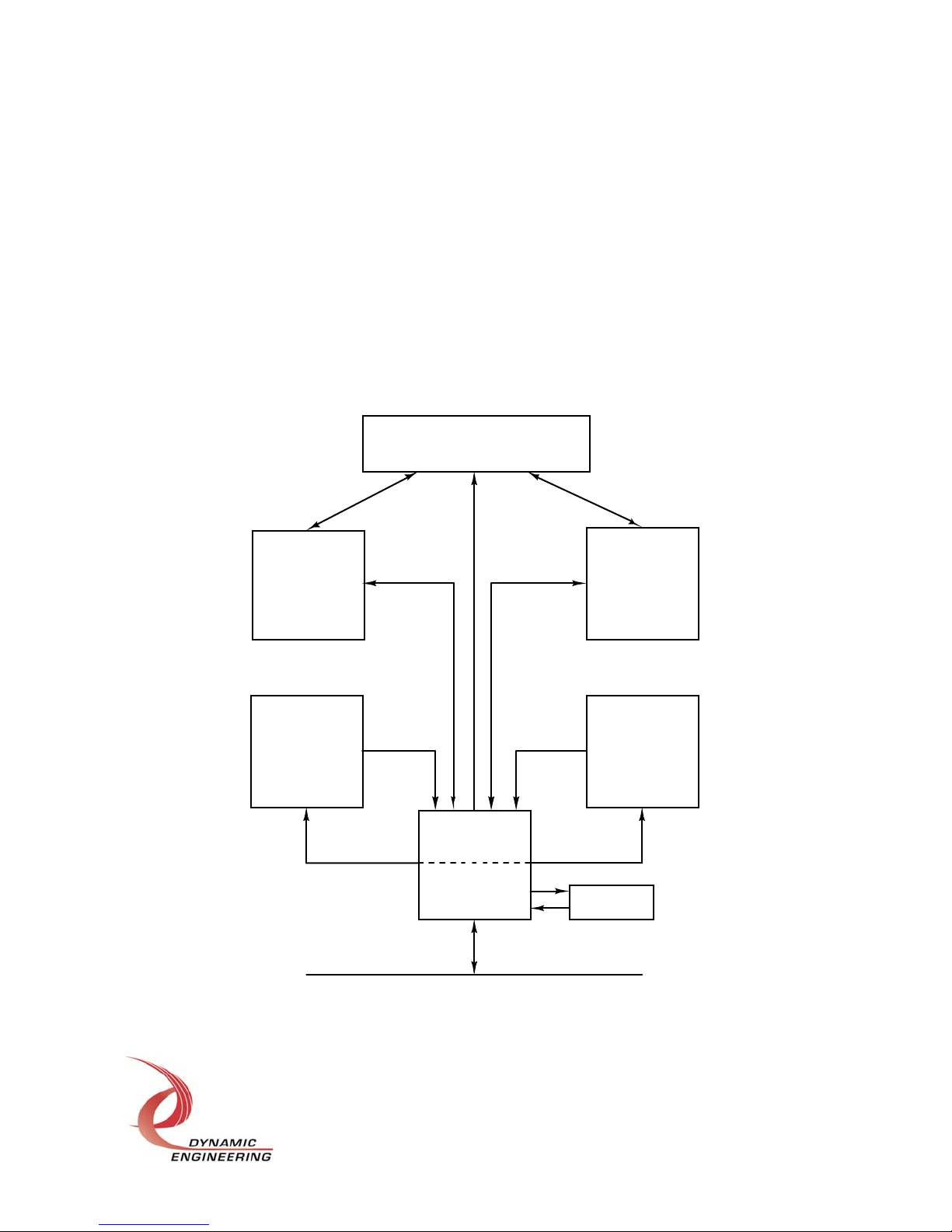
Product Description
The PMC BiSerial-III-HW2 is part of the PMC Module family of modular I/O components
by Dynamic Engineering. The PMC BiSerial-III is capable of providing multiple serial
protocols. The HW2 protocol implemented provides 8 Manchester encoded inputs and
outputs and 6 additional blocks that can each be configured as either one full-duplex
SDLC I/O or two full-duplex asynchronous (UART) I/O.
Other custom interfaces are available. We will redesign the state machines and create
a custom interface protocol. That protocol w ill t hen be offer ed as a “ s t andar d” special
order product. Please see our web page for current protocols offered. Please contact
Dynamic Engineering with your custom application.
485/LVDS buffers
termination
State
Machine
B
FIFO B
128K x 32
State
Machine
A
FIFO A
128K x 32
Data Flow
Control
PCI IF
PLL
FIGURE 1 PMC BISERIAL-III BASE BLOCK DIAGRAM
Embedded Solutions Page 6 of 50
Page 7
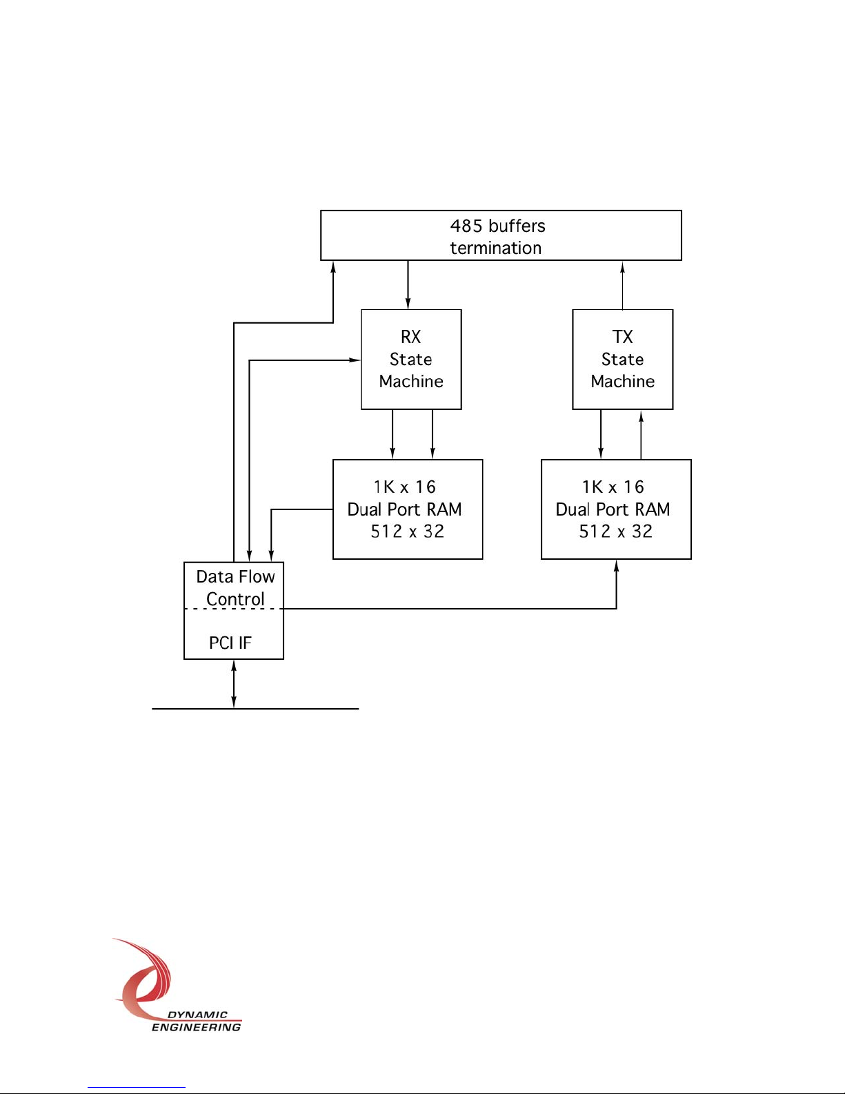
The standard configuration shown in Figure 1 makes use of two ext e r nal (to the Xilinx)
FIFOs. The FIFOs can be as large as 128K deep x 32 bits wide. Some designs do not
require so much memory, and are more efficiently implemented using the Xilinx internal
memory.
FIGURE 2 PMC BISERIAL-III-HW2 P2P BLOCK DIAGRAM
The HW2 implementation has 32 – Dual Port RAM (DPR) blocks implemented using
the Xilinx internal block RAM. Each channel has one or more associated DPRs
depending on which mode is active. Each DPR is configured to have a 32-bit port on
the PCI side, and a 16-bit port on the I/O side.
The lower eight channels are configured with the point-to-point interface that was used
on the HW1. In this mode when operating in the bidirectional mode the DPR is split in
half to provide both transmit, and receive buffers. I n t he unidirectional mode the full
DPR can be used for transmit or receive data.
Embedded Solutions Page 7 of 50
Page 8
The data rates are programmable to either 400 KHz or 5 MHz. Usually t he 5 MHz rate
is used in the unidirectional mode and the 400 KHz in the bidirectional mode. The data
is Manchester encoded. The hardware uses a higher rate clock to separate the clock
and data embedded within the Manchester data stream.
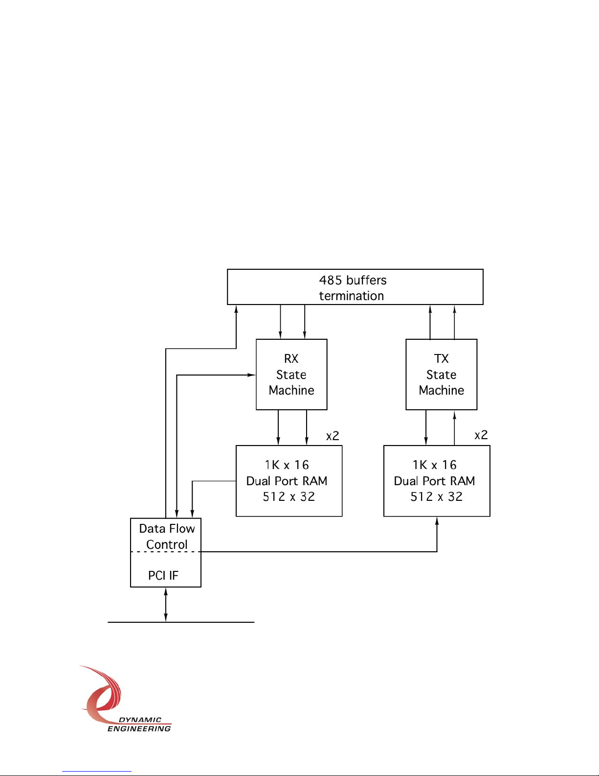
The remaining 24 channels are divided into six four-channel blocks that can each be
configured as either one full-duplex SDLC interface or two full-duplex asynchronous
interfaces.
The SDLC interface uses programmable PLL clock A as its reference frequency with
clock and data in and out comprising the four I/O lines of the channel block. The four
DPRs are partitioned into two blocks each for transmit and receive circular buffers that
have independently specified start and stop addresses and separate tr ansmit and
receive interrupts.
FIGURE 3 PMC BISERIAL-III-HW2 SDLC BLOCK DIAGRAM
Embedded Solutions Page 8 of 50
Page 9
Each asynchronous interface uses either programmable PLL clock B or a fixed 5 MHz
as its 16x reference frequency with data in and out using two of the four I/O lines of the
channel block. Two DPRs are used for each asynchronous interface, one each for
transmit and receive circular buffers that have independently specified start and stop
addresses.
FIGURE 4 PMC BISERIAL-III-HW2 ASYNC BLOCK DIAGRAM
The two asynchronous interfaces in a channel block are independently configurable
and each have separate receive and transmit interrupts.
All the data I/O lines on the HW2 are programmable to be register controlled or statemachine controlled. Any or all of the bits can be used as a parallel port instead of being
dedicated to a specific I/O protocol. Thirty-four differential I/O are provided at the front
bezel (32 of the 34 at Pn4) for the serial signals. The drivers and receivers conform to
the RS-485 specification (exceeds RS-422 specification). The RS-485 input signals are
selectively terminated with 100Ω. The termination resistors are in two-element
Embedded Solutions Page 9 of 50
Page 10

packages to allow flexible termination options for custom formats and protocols.
Optional pullup/pulldown resistor packs can also be installed to provide a logic ‘1’ on
undriven lines. The terminations and transceiv er s ar e pr ogr ammable t h r ough t he Xilinx
device to provide the proper mix of outputs and inputs and terminations needed for a
specific protocol implementation. The terminations are programmable for all I/O.
All configuration registers support read and write operations for maximum software
convenience, and all addresses are long word aligned.
The PMC BiSerial-III conforms to the PMC and CMC draft standards. This guarantees
compatibility with multiple PM C Car r ier boar ds. Because the PMC may be mounted on
different form factors, while maintaining plug and software compatibility, system
prototyping may be done on one PMC Carrier board, with final sy st em implementation
uses a different one.
The PMC BiSerial-III uses a 10 mm inter-board spacing for the front panel, standoffs,
and PMC connectors. The 10 mm height is the "st andar d" height and w ill work in most
systems with most carriers. If your carrier has non-standard connectors (height) to
mate with the PMC BiSerial-III, please let us know. We may be able to do a special
build with a different height connector to compensate.
Interrupts are supported by the PMC BiSerial-III-HW2. An interrupt can be configured to
occur at the end of a transmitted packet or message. An int er r upt will be set at the end
of a received packet or message. All interrupts are individually maskable, and a master
interrupt enable is also provided to disable all interrupts simultaneously. The current
status is available for the state-machines making it possible to operat e in a polled
mode. I2O interrupt processing is also available.
Embedded Solutions Page 10 of 50
Page 11

Theory of Operation
The PMC BiSerial-III-HW2 is designed for transferring data from one point to another
with three simple serial protocols.
The PMC BiSerial-III-HW2 features a Xilinx FPGA. The FPGA contains all of the
registers and protocol controlling elements of the BiSerial I II design. O nly the PLL,
transceivers, and switches are external to the Xilinx device.
The PMC BiSerial-III is a part of the PMC Module family of modular I/O products. It
meets the PMC and CMC draft Standards. In standard configuration, the PMC
BiSerial-III is a Type 1 mechanical with only low-profile components on the back of the
board and one slot wide, with 10 mm inter-board height. Contact Dy namic Engineering
for a copy of this specification. It is assumed t hat the reader is at least casually familiar
with this document and basic logic design.
The PCI interface to the host CPU is cont r olled by a logic block within the Xilinx. The
BiSerial III design requires one wait state for read or write cycles to any address. The
PMC BiSerial-III is capable of supporting 40 MBytes per second into and out of the
DPR. With a Windows® read/write loop better than 20 MB/sec is attained on most
computers. The wait states refer to the number of clocks after the PCI core decode
before the “terminate with data” state is reached. Two additional clock periods account
for the 1 clock delay to decode the signals from the PCI bus and to convert the
terminate with data state into the TRDY signal.
The BiSerial III can support many protocols. The PMC BiSerial-III-HW2 uses
Manchester serial encoded data and clock for its point-to-point interface. Data is sent
in 16-bit words; concatenated for multiple word transfers. The Manchester timing is
shown in the next diagram.
State machines within the FPGA control all transfers to and from the internal RAM and
I/O logic. The TX state machine reads from the transmit memory and loads the shift
registers before sending the data. The RX state machine receives data from the data
buffers and takes care of moving data from the shift register into the RX memory.
Data is read from the TX memory. The first two locations are control words. The
control words are stored for state-machine use. The first data word is then read and
loaded into the output shift register and the CRC generator. The Shift register is
enabled to shift the data out. As the bits are shifted out of the shift register the data is
encoded for Manchester compatibility. When the last data word has been loaded into
the CRC and shift register, the hardwar e completes the CRC processing to be prepared
for the last load to the shift register . O nce the CRC has been transmitted the hardware
checks to see if more data is to be sent or if this was the last packet in the message.
There are several options including using a softwar e CRC instead of the hardware
Embedded Solutions Page 11 of 50
Page 12

generated one, adding a post amble pattern etc. Please refer to the register bit
definitions for more details.
DATA IN/OUT
MANCHESTER ENCODING
0
10
0
011
0
11 0
10
FIGURE 5 PMC BISERIAL III HW2 MANCHESTER TIMING DIAGRAM
The receive function uses a free running shift register coupled with the receive statemachine to capture the data. When the receiver detects the idle pattern followed by 4
Manchester ‘0’s the receiver starts to capture data. The dat a is read in and st ored int o
the DPR. The embedded length is used to determine where t he CRC should be. The
CRC is calculated as the data is received and checked against the CRC received with
the packet. An error bit is set if the two do not match. Manchester errors within the
packet are detected, and used to abort processing of the message. After a packet has
been received the Post Amble is tested to see that it follows the proper protocol. The
Manchester and Post Amble errors are also latched in status bits.
This document is somewhat restricted as to the technical content allow ed in describing
the electrical interface. The document “Point-to-Point Data Bus Protocol Specification –
C72-1199-069” provides a more complete description of the interface.
The PMC BiSerial-III-HW2 also supports an SDLC interface. This is a synchronous
interface with separate clock and data inputs and outputs. Each message is delimited
by start/stop flag characters consisting of an eight-bit (0x7E) pattern. In order t o avoid
false flag detection from the data pattern, if five consecutive ones appear anyw here in
the data stream, an additional zero is inserted to avoid having six consecutiv e one bit s.
On the receive side, when five ones are received the sixth bit is monitored. I f it is a
zero, it is removed from the data stream, if it is a one then either a start/stop flag or an
abort character (0xFE) has been detected.
To send a message, write the message data to the transmit DPRs, specify the start and
stop addresses and configuration control bits, then enable the transmitter. The st at e-
Embedded Solutions Page 12 of 50
Page 13

machine will load the start address, send the opening flag charact er and begin sending
data sequentially LSB first until the end address is reached and the closing flag is sent.
If the TX clear is enabled, the transmitter will be automatically disabled when the
transmission is complete. Otherwise , t he transmitter will wait , pointing at the next
address after the end address. If additional data has been or is later written to t he
DPR, a new message can be started by entering a new end address. The tr ansmit
state-machine will then start a new message and cont inue sending data until the new
end address has been reached. If the end of the second DPR block is reached before
the end address, the transmitter will proceed to the beginning of the first DPR block and
continue until the end address is reached. Likewise when the end of the first DPR is
reached, the transmitter continues with the beginning of the second DPR.
To receive a message the receiver must be enabled, but only the st art ing address of
the receive buffer needs to be specified. Data w ill be stored sequentially starting at that
address until the closing flag is detected. This will latch an RX interrupt status and can
cause an interrupt if enabled. The last address that data (16-bit words) is st ored in is
latched and can be read from the control register as a read-only field.
The transmit interrupt is mapped to the first interrupt line of the channel block and the
receive interrupt is mapped to the second interrupt line. The remaining two int errupt
lines are not used in SDLC mode.
An asynchronous interface is also available on the PMC BiSerial-III-HW2. This protocol
uses one start-bit (low) eight data-bits no parity and one st op-bit (high). The marking
(idle) state of the line is high and eleven bit-periods of this high stat e w ill be interpreted
as the end-of-message condition.
The clock reference is supplied by either PLL clock B or 5 MHz derived from the onboard oscillator. This frequency is sixteen t imes the bit rate of the interface. The
transmit clock is derived by a straight divide-by sixteen circuit, while the receive statemachine uses the higher frequency to detect dat a bit s and will re-sync its clock counter
when detected data transitions are close but not exact ly on sixteen clock boundaries.
This allows for greater flexibility in matching transmitter and receiver clock frequencies.
Each asynchronous interface uses two DPR blocks, one for the transmitter and one for
the receiver. The process of sending and receiving messages is similar to the SDLC
interface except that only half as much memory is available for the receive and transmit
buffers. Also the receiver end address that is latched when a received message
completes is a byte address. That is the lower tw o bit s of the address specify which
byte was the last to be wr it t en, while the remaining address bits specify the 32-bit word
that contains that byte e.g. an end address of 0x3ff would indicate t hat all four bytes of
the 255
th
word of the receive DPR were written.
The transmit interrupt is mapped to the first or third interrupt line of the channel block
and the receive interrupt is mapped to the second or fourth interrupt line.
Embedded Solutions Page 13 of 50
Page 14

Address Map
BIS3_BASE 0x0000 0 Base control register
BIS3_ID 0x0004 1 ID register
BIS3_START_SET 0x0008 2 Start-bit set register
BIS3_START_CLR 0x000C 3 Start-bit clear register
BIS3_START_RDBK 0x0008 2 Start-bit read-back
BIS3_IO_DATA 0x0010 4 Data register 31 - 0
BIS3_IO_DIR 0x0014 5 Direction register 31 - 0
BIS3_IO_TERM 0x0018 6 Termination register 31 - 0
BIS3_IO_MUX 0x001C 6 Mux register 31 - 0
BIS3_IO_UCNTL 0x0020 8 Upper control register 33, 32
BIS3_STAT_FIFO 0x0024 9 User switch value
BIS3_PLL_CMD 0x0028 10 PLL control register and read-back of PLL data
BIS3_PLL_RDBK 0x002C 11 PLL control register read-back
BIS3_SM_CNTL_0 0x0040 16 Chan 0 state-machine control read-write port
BIS3_SM_CNTL_1 0x0044 17 Chan 1 state-machine control read-write port
BIS3_SM_CNTL_2 0x0048 18 Chan 2 state-machine control read-write port
BIS3_SM_CNTL_3 0x004C 19 Chan 3 state-machine control read-write port
BIS3_SM_CNTL_4 0x0050 20 Chan 4 state-machine control read-write port
BIS3_SM_CNTL_5 0x0054 21 Chan 5 state-machine control read-write port
BIS3_SM_CNTL_6 0x0058 22 Chan 6 state-machine control read-write port
BIS3_SM_CNTL_7 0x005C 23 Chan 7 state-machine control read-write port
BIS3_SDLC_CNTL_0 0x0060 24 Chan 8 SDLC control read-write port
BIS3_ASYNC_CNTL_0 0x0060 24 Chan 8 asynchronous control read-write port
BIS3_ASYNC_CNTL_1 0x0068 26 Chan 10 asynchronous control read-write port
BIS3_SDLC_CNTL_1 0x0060 28 Chan 12 SDLC control read-write port
BIS3_ASYNC_CNTL_2 0x0060 28 Chan 12 asynchronous control read-write port
BIS3_ASYNC_CNTL_3 0x0068 30 Chan 14 asynchronous control read-write port
BIS3_SDLC_CNTL_2 0x0070 32 Chan 16 SDLC control read-write port
BIS3_ASYNC_CNTL_4 0x0070 32 Chan 16 asynchronous control read-write port
BIS3_ASYNC_CNTL_5 0x0078 34 Chan 18 asynchronous control read-write port
BIS3_SDLC_CNTL_3 0x0080 36 Chan 20 SDLC control read-write port
BIS3_ASYNC_CNTL_6 0x0080 36 Chan 20 asynchronous control read-write port
BIS3_ASYNC_CNTL_7 0x0088 38 Chan 22 asynchronous control read-write port
BIS3_SDLC_CNTL_4 0x00A0 40 Chan 24 SDLC control read-write port
BIS3_ASYNC_CNTL_8 0x00A0 40 Chan 24 asynchronous control read-write port
BIS3_ASYNC_CNTL_9 0x00A8 42 Chan 26 asynchronous control read-write port
BIS3_SDLC_CNTL_5 0x00B0 44 Chan 28 SDLC control read-write port
BIS3_ASYNC_CNTL_10 0x00B0 44 Chan 28 asynchronous control read-write port
BIS3_ASYNC_CNTL_11 0x00B8 46 Chan 30 asynchronous control read-write port
Embedded Solutions Page 14 of 50
Page 15

BIS3_IO_RDBK 0x00C0 48 External I/O read register
BIS3_IO_RDBKUPR 0x00C4 49 External I/O upper bits read register
BIS3_CHAN_MODE 0x00C8 50 Channel mode control register
BIS3_INT_STAT 0x00CC 51 Interrupt status and clear register
BIS3_I2OAR 0x00D4 53 I2O address storage register
BIS3_SM_MEM_0 0x00800 Dual-port RAM 0 read/write port
BIS3_SM_MEM_1 0x01000 Dual-port RAM 1 read/write port
BIS3_SM_MEM_2 0x01800 Dual-port RAM 2 read/write port
BIS3_SM_MEM_3 0x02000 Dual-port RAM 3 read/write port
BIS3_SM_MEM_4 0x02800 Dual-port RAM 4 read/write port
BIS3_SM_MEM_5 0x03000 Dual-port RAM 5 read/write port
BIS3_SM_MEM_6 0x03800 Dual-port RAM 6 read/write port
BIS3_SM_MEM_7 0x04000 Dual-port RAM 7 read/write port
BIS3_SM_MEM_8 0x04800 Dual-port RAM 8 read/write port
BIS3_SM_MEM_9 0x05000 Dual-port RAM 9 read/write port
BIS3_SM_MEM_10 0x05800 Dual-port RAM 10read/write port
BIS3_SM_MEM_11 0x06000 Dual-port RAM 11 read/write port
BIS3_SM_MEM_12 0x06800 Dual-port RAM 12 read/write port
BIS3_SM_MEM_13 0x07000 Dual-port RAM 13 read/write port
BIS3_SM_MEM_14 0x07800 Dual-port RAM 14 read/write port
BIS3_SM_MEM_15 0x08000 Dual-port RAM 15 read/write port
BIS3_SM_MEM_16 0x08800 Dual-port RAM 16 read/write port
BIS3_SM_MEM_17 0x09000 Dual-port RAM 17 read/write port
BIS3_SM_MEM_18 0x09800 Dual-port RAM 18 read/write port
BIS3_SM_MEM_19 0x0A000 Dual-port RAM 19 read/write port
BIS3_SM_MEM_20 0x0A800 Dual-port RAM 20 read/write port
BIS3_SM_MEM_21 0x0B000 Dual-port RAM 21 read/write port
BIS3_SM_MEM_22 0x0B800 Dual-port RAM 22 read/write port
BIS3_SM_MEM_23 0x0C000 Dual-port RAM 23 read/write port
BIS3_SM_MEM_24 0x0C800 Dual-port RAM 24 read/write port
BIS3_SM_MEM_25 0x0D000 Dual-port RAM 25 read/write port
BIS3_SM_MEM_26 0x0D800 Dual-port RAM 26 read/write port
BIS3_SM_MEM_27 0x0E000 Dual-port RAM 27 read/write port
BIS3_SM_MEM_28 0x0E800 Dual-port RAM 28 read/write port
BIS3_SM_MEM_29 0x0F000 Dual-port RAM 29 read/write port
BIS3_SM_MEM_30 0x0F800 Dual-port RAM 30 read/write port
BIS3_SM_MEM_31 0x10000 Dual-port RAM 31 read/write port
FIGURE 6 PMC BISERIAL-II
I-HW2 INTERNAL ADDRESS MAP
The address map provided is for the local decoding performed within the PMC BiSerialIII. The addresses are all offsets from a base address, which is assigned by the system
when the PCI bus is configured.
Embedded Solutions Page 15 of 50
Page 16

Programming
Programming the PMC BiSerial-III-HW2 requires only the ability to read and w r it e data
from the host. The base address of the module refers to the first user address for the
slot in which the PMC is installed. This address is determined during system
configuration of the PCI bus.
Depending on the software environment it may be necessary to set - up t he system
software with the PMC BiSerial-III "registration" data. For example in WindowsNT there
is a system registry, which is used to identify t he resident hardware.
In order to receive data the software is only required to enable t he Rx channel and set
the frequency parameters. To transmit the software will need to load t he message int o
the appropriate Dual Port RAM, set the frequency and mode and enable the transmitter.
The interrupt service routine should be loaded and the interrupt mask set. The interrupt
service routine can be configured to respond to the channel interrupts on an individual
basis. After the interrupt is received, the dat a can be ret r ieved. An efficient loop can
then be implemented to fetch the data. New messages can be received even as t he
current one is read from the Dual Port RAM.
The TX interrupt indicates to the software that a message has been sent and t hat t he
message has completed. If more than one interrupt is enabled, then the interrupt
service routine (ISR) needs to read the status to see w hich source caused the interrupt.
The status bits are latched, and are explicitly cleared by writing a one to the
corresponding bit. It is a good idea to read the status register and write that value back
to clear all the latched interrupt status bit s befor e st ar ting a transfer. This will insure
that the interrupt status values read by the ISR came from the current transfer.
Refer to the Theory of Operation section above and the Interrupt s sect ion below for
more information regarding the exact sequencing and interrupt definitions.
The VendorId = 0x10EE. The CardId = 0x002E.
Flash design ID = 0x0002, Current Flash revision = 0x0002
Embedded Solutions Page 16 of 50
Page 17

Register Definitions
BIS3_BASE
[$00] BiSerial III Base Control Register Port read/write
Base Control Register
DATA BIT DESCRIPTION
31-4 Spare
3 I2O CLR
2 I2O EN
1 Interrupt Set
0 Interrupt Enable Master
FIGURE 7 PMC BISERIAL-III BASE CONTROL REGISTER BIT MAP
All bits are active high and are reset on power-up or reset command.
Interrupt Enable Master : When '1' allows interrupts generated by the
PMC-BiSerial-III-HW2 to be driven onto the carrier (INTA). When '0' the interrupts can
be individually enabled and used for status without driving the backplane. Polled
operation can be performed in this mode.
Interrupt Set : When '1' and the Master is enabled, this bit forces an interrupt request.
This feature is useful for testing and software development.
I2O EN : When ‘1’ allows the I2O interrupts to be activated. I nt errupt request s are
routed to the address stored in the I2O Address Register (I2O AR). When ‘0’ the I2O
function is disabled.
I2O CLR : When ‘1’ this bit will cause the current data stored in the I 2O collect ion
register to be cleared. It is recommended that this register clear bit be used
immediately before enabling I2O operation to prevent previously stored events from
causing interrupts.
Embedded Solutions Page 17 of 50
Page 18

BIS3_ID
[$04] BiSerial III FLASH status/Driver Status Port read only
Design Number / FLA SH Revision
DATA BIT DESCRIPTION
31-16 Design/Driver ID
15-0 FLASH revision
FIGURE 8 PMC BISERIAL-III DESIGN ID REGISTER BIT MAP
The Design / Driver ID for the HW2 project is 0x0002. The FLASH ID will be updated
as features are added or revisions made. See the programming section for the current
FLASH revision.
BIS3_START_SET
BIS3_START_RDBK
[$08] BiSerial III Start Set Control Register Port read/write
Start Set Register
DATA BIT DESCRIPTION
7-0 Channels to activate (write only)
7-0 Channels that are active (read only)
FIGURE 9 PMC BISERIAL-III START SET REGISTER
To start a channel, write a ‘1’ to the corres ponding bit . To clear a channel use t he St art
Clear register. Read back from this port reflects the channels which are active. Please
note that channel these bits can be cleared by the channel stat e-machines.
Embedded Solutions Page 18 of 50
Page 19

BIS3_START_CLR
[$0C] BiSerial III Start Clear Control Register Port write only
Start Clear Register
DATA BIT DESCRIPTION
7-0 Clear the active Start Bits
FIGURE 10 PMC BISERIAL-III START CLEAR REGISTER
Writ ing a ‘1’ t o a channel clear bit will cause that channels Start Bit to be clear ed. The
Channel will complete the current operation and t hen abor t pr ocessing. Reading fr om
the RDBK register will show the active channels. The state-machine may be running at
a significantly slower rate than the PCI bus. There may be some delay in sensing that
the start abort has been set for a particular channel.
The delay can be estimated to be the period of the clock in use and 12 periods. For
transmit the clock rate is 2x the data rate. For receive the clock rate is 8x the data rate.
At low speed in transmit mode the delay would be 12x (1/800 Khz ) = > 15 uS or so.
These are worst case delays.
Please note that the “ready_busy” bit can be used t o check when an aborted channel is
ready for a new start command. Please refer to the channel control registers.
Embedded Solutions Page 19 of 50
Page 20

BIS3_IO_DATA
[$10] BiSerial III Parallel Data Output Register read/write
Parallel Data Output Register
DATA BIT DESCRIPTION
31-0 parallel output data
FIGURE 11 PMC BISERIAL-III PARALLEL OUTPUT DATA BIT MAP
There are 32 potential output bits in the parallel port. The Direction, Termination, and
Mux Control registers are also involved. When the direction is set to output, and the
Mux control set to parallel port the bit definitions from this register are driven onto the
corresponding parallel port lines.
This port is direct read-write of the register. The I/O side is read-back from the
BIS3_IO_RDBK port. It is possible that t he output data does not match the I/O data in
the case of the Direction bits being set to input or the Mux control set t o st at e-machine.
BIS3_IO_DIR
[$14] BiSerial III Direction Port read/write
Direction Control Port
DATA BIT DESCRIPTION
31-0 Parallel Port Direction Control bits
FIGURE 12 PMC BISERIAL-III DIRECTION CONTROL PORT
When set (‘1’) the corresponding bit in the parallel port is a transmitter. When cleared
(‘0’) the corresponding bit is a receiver. The corresponding Mux control bits must also
be configured for parallel port.
Embedded Solutions Page 20 of 50
Page 21

BIS3_IO_TERM
[$18] BiSerial III Termination Port read/write
Direction Control Port
DATA BIT DESCRIPTION
31-0 Parallel Port Terminat ion Control bit s
FIGURE 13 PMC BISERIAL-III TERMINATION CONTROL PORT
When set (‘1’) the corresponding I/O line will be terminated. When cleared (‘0’) the
corresponding I/O line is not terminated. These bits are independent of the Mux control
definitions. When a bit is set to be terminated; the analog switch associated with that
bit is closed to create a parallel termination of approximately 100 Ω. In most systems
the receiving side is terminated, and the transmitting side is not. The drivers can
handle termination on both ends.
BIS3_IO_MUX
[$1C] BiSerial III Mux Port read/write
Direction Control Port
DATA BIT DESCRIPTION
31-0 Parallel Port Mux Control bits
FIGURE 14 PMC BISERIAL-III MUX CONTROL PORT
When set (‘1’) the corresponding bit is set to State-Machine control. When cleared (‘0’)
the corresponding bit is set to parallel port operation. The Mux cont rol definition along
with the Data, Direction and Termination registers allows for a bit-by-bit selection of
operation under software control.
Embedded Solutions Page 21 of 50
Page 22

BIS3_IO_UCNTL
[$20] BiSerial III Upper Control Port read/write
Upper Bits Control Port
DATA BIT DESCRIPTION
25-24 Mux 33,32
17-16 Termination 33,32
9-8 Direction 33,32
1-0 Data 32,32
FIGURE 15 PMC BISERIAL-III UPPER CONTROL PORT
The BiSerial III has 34 transceivers. The upper control bits are concentrated within this
register to cover the top 2 bits not controlled wit hin t he ot her cont rol regist ers. The
upper bits are only useable on the Bezel I/O connect or. Pn4 has only 64 connections
and doesn’t support the upper lines. The definitions are the same as the Data, Term,
Dir and Mux port definitions for bit operation.
Data = Data transmitted when the Mux is set to ‘0’ and the direction is set to ‘1’.
Termination when set to ‘1’ causes the parallel termination to be engaged. Sett ing the
Mux control bits to ‘0’ creates a parallel port for those bits. Sett ing t he Mux cont rol bit s
to ‘1’ enables the state-machine to control the direction and data lines. The termination
control is independent.
BIS3_IO_RDBK
[$C0] BiSerial III I/O Read-Back Port read only
I/O Read-Back Port
DATA BIT DESCRIPTION
31-0 I/O Data 31-0
FIGURE 16 PMC BISERIAL-III I/O READBACK PORT
The I/O lines can be read at any time. The value is not filtered in any way. If the
transceivers are set to TX by the parallel port or st at e-machine then the read-back
value will be the transmitted value. If t he t r ansceivers are set to receive then t he por t
values will be those received by the t r ans ce ivers from the external I/O.
Embedded Solutions Page 22 of 50
Page 23

BIS3_IO_RDBKUPR
[$C4] BiSerial III I/O Upper Read-Back Port read only
I/O Upper Read-Back Port
DATA BIT DESCRIPTION
1-0 I/O Data 33-32
FIGURE 17 PMC BISERIAL-III I/O READBACK PORT
The I/O lines can be read at any time. The value is not filtered in any way. If the
transceivers are set to TX by the parallel port or st at e-machine then the read-back
value will be the transmitted value. If t he t r ansceivers are set to receive then t he por t
values will be those received by the t r ans ce ivers from the external I/O. The upper bits
are presented on this port.
BIS3_STAT_FIFO
[$24] BiSerial III Switch Port read only
User Switch Port
DATA BIT DESCRIPTION
31-24 Spare
23-16 sw7-0
15-0 Spare
FIGURE 18 PMC BISERIAL-III SWITCH PORT
The Switch Read Port has the user bits. The user bits are connected t o the eight dipswitch positions. The switches allow custom configurations to be defined by t he user
and for the software to identify a particular board by its swit ch set t ings and t o configure
it accordingly.
1
0
The Dip-switch is marked on the silk-screen with the positions of
the digits and the '1' and '0' definitions. The numbers are hex
coded. The example shown would produce 0x12 when read (and
70
shifted down).
Embedded Solutions Page 23 of 50
Page 24

BIS3_PLL_CMD, PLL_RDBK
[$28, 2C] BiSerial III PLL Control
PLL Command Register, PLL CMD Read-ba ck
DATA BIT DESCRIPTION
3 PLL Enable
2 PLL S2
1 PLL SCLK
0 PLL SDAT
FIGURE 19 PMC BISERIAL-III PLL CONTROL
The register bits for PLL Enable, PLL S2, PLL SCLK are unidirectional from t he Xilinx to
the PLL – always driven. SDAT is open drain. The SDAT regist er bit when written low
and enabled will be reflected with a low on the SDAT signal to t he PLL. When SDAT is
taken high or disabled the SDAT signal will be tri-stated by the Xilinx, and can be dr iven
by the PLL. The SDAT register bit when read reflects the stat e of the SDAT signal
between the Xilinx and PLL and can be in a different state than the written SDAT bit.
To read back the contents of the CMD port use the RDBK port.
PLL Enable : When this bit is set to a one, SDAT is enabled. When set to ‘0’ SDAT is
tri-stated by the Xilinx.
SCLK/SDAT : These signals are used to program the PLL over the I2C serial
PLL
interface. SCLK is always an output whereas
SDAT is bi-directional. When SDAT is to
be read from the
PLL S2 : This is an additional control line to the PLL that can be used to select
alternative pre-programmed frequencies.
The PLL is a separate device controlled by t he Xilinx. The PLL has a fairly complex
programming requirement which is simplified by using the Cypress® CyberClocks
utility, and then programming t he r esulting control words into the PLL using this PLL
Control port. The interface can be further simplified by using the Dynamic Engineering
driver to take care of the low-level bit manipulation requirements.
Embedded Solutions Page 24 of 50
Page 25

BIS3_SM_CNTL7-0
[$5C, 58, 54, 50, 4C, 48, 44, 40] BiSerial III HW2 Control Registers (Active when mode = “10”)
State Machine Control Registers
DATA BIT DESCRIPTION
31 Ready_Busy (read only)
30 Manchester Error Status / CLR
29-20 Address Pointer (read only)
19 Post Amble Status / CLR
18 CRC Error Status / CLR
17-8 End of Message
5 INTEN
4 CLREN
3 Bi_Uni
2 IDLE Pattern Transmit
1 HI_LOW Speed
0 TX/RX Operation
FIGURE 20 PMC BISERIAL-III STATE MACHINE CONTROL REGISTERS
Each state-machine has a separate control register to govern the operation of the
channel. In addition, the TX channels have control via the data in the Dual Port RAM
associated with that channel.
TX/RX when set ‘1’ indicates transmit operation. When cleared ‘0’ indicates receiver
operation.
HI_LOW when set ‘1’ indicates operation at t he “high speed” = 5 MHz nominal. In Low
speed mode ‘0’ the system operates at 400 Khz.
Bi_Uni when set ‘1’ indicates that bidirect ional operation is request ed. When cleared
‘0’ unidirectional operation is selected. In Bidirectional operation the memory is set to
operate with the lower half allocated to TX and the upper half to RX. The counter will
roll over to the correct boundaries (end of memory to 1/2, and 1/2 – 1 to start or end of
memory to start) based on the mode of operation. Continuous operation is possible.
In BiDirectional mode the transmitter is only enabled when transmitting. When the
transmission is completed the hardware automatically clears the TX bit and restarts in
RX mode (BiDir only) without clear ing t he start bit. This allows a response, and w ait for
data without software intervention.
In Unidirectional mode the transmitter is enabled whenever there is data to send or the
idle pattern is sent (if enabled). The tr ansmit t e r w ill send as many packets as the
Embedded Solutions Page 25 of 50
Page 26

hardware is programmed to send, and at the end of the message clear the start bit.
The hardware will remain in transmit or receive mode until changed by softwa r e.
IDLE when ‘1’ and in transmit mode commands the state-machine to insert the idle
pattern when not sending data from the Dual Por t RAM . In receive or BiDirectional
mode this bit should be set to zero.. When in transmit mode, and this bit is cleared the
transmitter is tri-stated between messages sent.
CLREN when set, and in transmit mode allows the start bit t o be cleared at t he end of a
message sent. Note that the start bit is not cleared unt il t he last packet of the message
is sent. For Rx this bit has no effect.
Please note that in BiDirectional mode this bit should be set and t he packet and end of
message addresses should be the same to cause a single packet to be sent and the TX
bit to be reset.
INTEN when set in RX or TX mode allows the channel to create an interrupt request.
The INTEN signal is applied after the holding register and before the interrupt request
to the PCI bus.
In TX mode there is a control bit in the DPR command that controls the interrupt to t he
packet level. In RX mode the interrupt is set for each packet received. In either case
the interrupt is generated by the state machine, and capt ured by the interrupt holding
register. By reading BIS3_INT_STAT the interrupt source(s) can be checked.
If INTEN is not set then the Interrupt status register can be used to poll for status. With
individual INTEN bits each channel can be operated in polled or interrupt driven modes.
To use the interrupt method the master interrupt enable must also be enabled.
End of Message is the address to test the address pointer against for the end of
message. A message is a group of packets. The packet length is embedded in the
message. Please refer to the Memory section for more details on the packet length
control. As each packet is sent the hardware tests the end of message address to
determine if there are more packets to send.
The end of packet address includes the command word through the CRC. St ar t ing w ith
‘0’ at the lower command word, and count ing n 16 bit dat a words plus the CRC plus 1 =
the end of packet address. When the end of message address matches the end of
packet address the hardware recognizes that the last packet processing should occur.
The command word is 32 bits and takes 2 locations. The offset (for post increment),
label, length, and CRC take 1 each for a total of 6 –1 = 5 ( count from zero) plus the
data length. For a message with 8 locations the end of packet address would be “D”.
Embedded Solutions Page 26 of 50
Page 27

The Address Pointer is stored w hen an interrupt condition happens during a read.
The address location stored is the address on the State-machine side of the Dual Port
RAM. In receive mode an interrupt is generated each time a packet is received or a
Manchester error is found. If the length is not incrementing to match the packet length
received then a Manchester error has occurred cutting the packet short. The hardware
will recover and look for the next packet. The address stored is t he next address where
data would be stored independent of LW boundaries. The next address used will be on
a long word boundary. The value will be valid until the next interrupt condit ion occur s.
Manchester Error, CRC Err or, Post Amble Error bit are set when the associat ed er r or is
detected.
The Manchester error is set when an illegal Manchester encoding happens w hen
properly coded data is expected. For example if a message is programmed to be of
one length and a shorter length is received the M anchest e r bit will be set because the
data will become the idle pattern ( t oo w ide bit per iods) or fix ed at 0 or 1.
The CRC error is set when the r eceived CRC does not match the calculated CRC.
The Post Amble error is set when the Post Amble pattern is not detected at the end of
a packet.
All three bits are cleared by writing w ith a ‘1’ in t he respect ive bit positions.
Ready_Busy when set indicates that the hardware is ready for a new start command.
When cleared the hardware is executing a command. For example: in tx mode with the
idle pattern turned on and unidirectional mode, the hardware will be ready while
sending the idle pattern. The transmitt er is active, but filling time and can accept a new
start command. Once start is set , the hardware will begin transmission the st at us will
change to Busy.
Embedded Solutions Page 27 of 50
Page 28

BIS3_SDLC_CNTL5-0
[$B0, A0, 90, 80, 70, 60] BiSerial III HW2 SDLC Control Registers (Active when mode = “00”)
SDLC Control Registers
DATA BIT DESCRIPTION
30 Abort Detected/Clear
29-19 Receive End Address (read only)
19 Send an Abort (write only)
18-8 Address Input
7 Load Transmit End Address
6 Load Transmit Start Address
5 Load Receive Start Address
4 Receive Interrupt Enable
3 Transmit Interrupt Enable
2 Transmit Clear Enable
1 Receive Enable
0 Transmit Enable
FIGURE 21 PMC BISERIAL-III SDLC CONTROL REGISTERS
Transmit Enable : When this bit is a one the transmitter is enabled to send data
starting with the address stored in the transmitter start-address regist er and cont inuing
until the data at the address in the transmitter end-address register has been sent.
When this bit is a zero the transmitter is disabled.
Receive Enable : When this bit is a one the receiver is enabled to receive data and
store it in the dual-port RAM starting with the address stored in the receiver startaddress register if it is the first message since the receiver was enabled, or in the next
16-bit address after the end-address of the last message if it is not. When this bit is a
zero the receiver is disabled.
Transmit Clear Enable : When this bit is a one the transmit enable bit will be cleared
when the transmitted message completes. When this bit is a zero the transmitter will
remain enabled, but no more data will be sent unless a new end address is loaded.
Transmit Interrupt Enable : When this bit is a one the transmitter interrupt is enabled.
The interrupt will occur at when t he t r ansmit st ate-machine reaches the end address
stored in the transmitter end-address register. When this bit is a zero the interrupt
status will still be latched, but w ill not cause an interrupt to occur. The tr ansmit interrupt
is mapped to the first interrupt line in its channel block.
Embedded Solutions Page 28 of 50
Page 29

Receive Interrupt Enable : When this bit is a one the receiver interrupt is enabled.
The interrupt will occur at the end of a message t r ansmission, which is determined by
the detection of a SDLC flag character (0x7e) after the message has started. When
this bit is a zero the interrupt status will still be latched, but will not cause an int e r r upt t o
occur. The receive interrupt is mapped to the second interrupt line in its channel block;
the remaining two interrupt lines are not used in SDLC mode.
Load Receive Start Address : When this bit is a one the value in the address input
field is loaded into the receiver start-address register. When this bit is a zero no action
is taken.
Load Transmit Start Address : When this bit is a one the value in the address input
field is loaded into the transmitter start-address register. When this bit is a zero no
action is taken.
Load Transmit End Addr ess : When this bit is a one the value in the address input
field is loaded into the transmitter end-address register. When this bit is a zero no
action is taken.
Address Input : This field is used with the t hree load address bit s t o specify address
boundaries for the transmit and receive state machines.
Send an Abort : When this bit is set to a one the transmit state-machine will send an
abort character (0xfe) provided a transmission is currently in progress. When this bit is
a zero normal operation will continue.
Receive End Address : This field represents the address that the last received data
word is stored in. Note that this is a 16-bit address, bit 0 indicat es which half of the
appropriate long-word the last 16-bit word was stored (0 -> lower half, 1 -> upper half).
Abort Detected : When an abort character is detected by the receiver, this status bit
will be latched and can be cleared by writing a one back in this bit posit ion.
Embedded Solutions Page 29 of 50
Page 30

BIS3_ASYNC_CNTL11-0
[$B8, B0, A8, A0, 98, 90, 88, 80, 78, 70, 68, 60] BiSerial III HW2 Asynchronous Control
Registers (Active when mode = “01”)
Asynchronous Control Registers
DATA BIT DESCRIPTION
30 Framing Error/Clear
29-19 Receive End Address (read only)
18-9 Address Input
8 Clock Select
7 Load Transmit End Address
6 Load Transmit Start Address
5 Load Receive Start Address
4 Receive Interrupt Enable
3 Transmit Interrupt Enable
2 Transmit Clear Enable
1 Receive Enable
0 Transmit Enable
FIGURE 22 PMC BISERIAL-III SDLC CONTROL REGISTERS
Transmit Enable : When this bit is a one the transmitter is enabled to send characters
starting with the address stored in the transmitter start-address regist er and cont inuing
until the data in the transmitter end-address register has been sent. When this bit is a
zero the transmitter is disabled.
Receive Enable : When this bit is a one the receiver is enabled to receive characters
and store them in the dual-port RAM starting with the address stored in the receiver
start-address register if it is the first message since the receiver was enabled, or in the
next 16-bit address after the end-address of the last message if it is not. When this bit
is a zero the receiver is disabled.
Transmit Clear Enable : When this bit is a one the transmit enable bit will be cleared
when the transmitted message completes. When this bit is a zero t he t r ansmit ter will
remain enabled, but no more data will be sent unless a new end address is loaded.
Transmit Interrupt Enable : When this bit is a one the transmitter interrupt is enabled.
The interrupt will occur at when t he t r ansmit st ate-machine reaches the end address
stored in the transmitter end address register. When this bit is a zero the interrupt
status will still be latched, but w ill not cause an interrupt to occur. The tr ansmit interrupt
is mapped to the first or third interrupt line in its channel block depending on whether it
is the first or second asynchronous interface in that block.
Embedded Solutions Page 30 of 50
Page 31

Receive Interrupt Enable : When this bit is a one the receiver interrupt is enabled.
The interrupt will occur at the end of a message t r ansmission, which is determined by
the detection of at least eleven bit-periods of a high level on the input line after a
message has started. When this bit is a zero the interrupt stat us will still be latched, but
will not cause an interrupt to occur. The r e ceive interrupt is mapped to the second or
fourth interrupt line in its channel block depending on whether it is the first or second
asynchronous interface in that block.
Load Receive Start Address : When this bit is a one the value in the address input
field is loaded into the receiver start-address register. When this bit is a zero no action
is taken.
Load Transmit Start Address : When this bit is a one the value in the address input
field is loaded into the transmitter start-address register. When this bit is a zero no
action is taken.
Load Transmit End Addr ess : When this bit is a one the value in the address input
field is loaded into the transmitter end-address register. When this bit is a zero no
action is taken.
Clock Select : When this bit is a one the PLL B clock input is selected as the 16x clock
for asynchronous character decoding. When this bit is a zero the 5 MHz clock is used
(312.5 Kbps). The clock is divided by sixteen to create the transmit bit clock.
Address Input : This field is used with the t hree load address bit s t o specify address
boundaries for the transmit and receive state machines.
Receive End Address : This field represents the address t hat t he last received
character is stored in. Note that this is a byt e address, t he lower two bits indicate the
byte (0 – 3) in the appropriate long-word where the last character w as st ored
Framing Error : When a one is read in this bit position, it indicates that a framing error
has been detected. This will occur if the stop bit for a r eceived character is not a one.
This bit is latched and is cleared by writing a one back in this bit posit ion.
Embedded Solutions Page 31 of 50
Page 32

BIS3_CHAN_MODE
[$C8] BiSerial III HW2 Channel Mode Control Register
Channel Mode Control Register
DATA BIT DESCRIPTION
31-16 Spare
15-14 Channel 31-28 mode (bit 15 = ‘0’)
13-12 Channel 27-24 mode (bit 13 = ‘0’)
11-10 Channel 23-20 mode (bit 11 = ‘0’)
9-8 Channel 19-16 mode (bit 9 = ‘0’)
7-6 Channel 15-12 mode (bit 7 = ‘0’)
5-4 Channel 11-8 mode (bit 5 = ‘0’)
3-2 Channel 7-4 mode = “10”
1-0 Channel 3-0 mode = “10”
FIGURE 23 PMC BISERIAL-III CHANNEL MODE CONTROL REGISTER
The first two channel blocks (channels 0 - 7) are “hard-wired” to HW1 mode. The
remaining six channel blocks can each be configured to be one full-duplex SDLC
channel using four I/O lines and four DPR blocks (2 each for transmit and receive) or
two full-duplex asynchronous channels each using two I/O lines and two DPR blocks (1
each for transmit and receive).
The mode definitions for each channel block are as follows:
One SDLC channel = “00”
Two ASYNC channels = “01”
Four HW1 channels = “10”
Embedded Solutions Page 32 of 50
Page 33

BIS3_INT_STAT
[$CC] BiSerial III Interrupt Status and Clear Register
Interrupt Status and Clear Register
DATA BIT DESCRIPTION
31-0 Channel Interrupt or Clear bit
FIGURE 24 PMC BISERIAL-III INTERRUPT STATUS REGISTER
Each bit is set when an interrupt occurs on the associated channel. Each bit can be
cleared by writing to the register w ith t he same bit position set (‘1’). You do not need to
rewrite with a ‘0’ – the clearing action happens during the wr it e.
This register is in parallel with the I2O interrupts. Usually only one or t he ot her will be in
use at a time. Both can be used if desired. Interrupt conditions are captured and
processed in both places.
BIS3_I2OAR
[$D4] BiSerial III I20 Address Register
I2O Address Register
DATA BIT DESCRIPTION
31-0 Address
FIGURE 25 PMC BISERIAL-III I2O ADDRESS REGISTER
The physical address where the I2O interrupt status should be written to is stored in this
register. When active interrupts are detected the I2O sequence is started. The PCI bus
is requested, the hardware waits for the grant and then wr it es t he capt ured status to the
stored address. Please note that this is the direct hardw are address, and not an
indirect (translated) address.
The active bits are auto cleared and the process re-enabled for new active interrupts.
Interrupts that occur during an I2O cycle are stored until the hardware is re-enabled and
cause a second immediate processing cycle. The receiving hardware must be able to
handle multiple interrupt status writes in close succession. A FIFO is ideal for the
receiving hardware implementation.
Embedded Solutions Page 33 of 50
Page 34

BIS3_SM_MEM31-0
[$0x800 – 0x10000] BiSerial III HW2 Dual Port RAM address space
The following discussion applies to the HW1 operating mode only. In SDLC or
asynchronous mode the DPRs are used to store I/O data only and each DPR is always
used as either a receive buffer or a transmit buffer, but never both.
Each channel has Dual Port RAM (DPR) associated with it. The DPR is configured to
have a 32-bit port on the PCI side and a 16-bit port on the I/O side. Each DPR is 1K x
16 on the I/O side and 512 x 32 on the PCI side.
When using BiDirectional mode the memory is further divided with an upper half and a
lower half. The lower half is used for transmit and the upper half for receive data. The
first 256 locations are used for TX and the upper 256 for r eceive in BiDirectional mode.
In Unidirectional Mode the memory is all allocated to either RX or TX, and starts at
offset 0x00.
The DPR is used to store the packet or packets of data to be transmitted or that have
been received. When transmitting the data should be loaded prior to starting. It is
possible to load additional data while transmitting if the software has tight cont rol over
the system timing.
In transmit the first 32 bits are the control word. The packet follows: Label, length, data,
CRC. The CRC will normally be Set to 0x00 and t he har dw ar e instructed to create and
insert the CRC.
Location I/O Value
0 lower command
1 upper command
2 label
3 length
4 First data
…
N last data
N+1 CRC or zero data
Location PCI
0 upper lower command
1 length label
2 data 1 data 0
…
N CRC data last or data last data last –1
XXXX CRC
Embedded Solutions Page 34 of 50
Page 35

When the CRC falls on a non 32-bit boundary; the last location is padded, and the
hardware will automatically skip that location to start on the new LW boundary.
The upper and lower command words are used to provide control on a packet-bypacket basis.
31 spare
30 Interrupt Enable
29 Post Amble Generation
28 CRC in Hardware
27-26 spare
25-16 spare
15-10 spare
9-0 End of Packet Address
The end of packet address and the end of message address are the word addresses on
the I/O side. The address is relative to the start of each DPR section – always starts at
0x00 and ends at 0x3ff for the 1K space.
The hardware will transmit until t he end of packet address is det ected. The hardware
will then either stop or start a new packet based on t he end of message address. The
end of message address is not checked until the end of packet, and is checked as an
absolute rather than a >= to allow roll over addressing t o be used.
At the end of the packet if the Interrupt Enable bit is set an interrupt request will be
generated. Each packet can have a different setting for this bit. Once at the end of
message, interrupt on every packet, alternat e packets etc.
At the end of the packet the hardware can append the post amble as defined in the
specification. If the bit is set the post amble will be added to the packet befor e going t o
tristate, or to the idle pattern if completed, or sending the next packet if more packets
are queued. If the bit is not set the post amble is ignored and the next process start ed
earlier.
If the CRC in hardware bit is set then the CRC is generated by t he har dware and
appended to the message. If the bit is not set t hen t he CRC is loaded fr om t he location
in memory immediately following the data. In either case a CRC is sent. To create a
CRC error on a given packet set the bit to “ memory supplied” and provide a bogus CRC
value for the data. With the per packet control one packet can be made bad and the
rest good to test error detection and response. Due to the processing required the
Hardware option will be the “nor mal” option.
Due to preprocessing and hardware timing constraints the address the hardware is
working with leads the data currently being sent. The following example w ill help t o
Embedded Solutions Page 35 of 50
Page 36

define the End of packet and end of message address as well as the CRC processing.
i = 0x00;
*pmcbis3SM_mem_0 = 0x7000000d; // stop after 1 pkt enable interrupt, post amble
generation, crc hardware generation, 1 packet stopping at address d
i = 0x01;
*(pmcbis3SM_mem_0 + i) = 0x00080400; // length label 0008 0400
i = 0x02;
*(pmcbis3SM_mem_0 + i) = 0x5555aaaa; // data 2 data 1
i = 0x03;
*(pmcbis3SM_mem_0 + i) = 0x0000ffff; // data 4 data 3
i = 0x04;
*(pmcbis3SM_mem_0 + i) = 0xaaaa1234; // data 6 data 5
i = 0x05;
*(pmcbis3SM_mem_0 + i) = 0x5555aaaa; // data 8 data 7
i = 0x06;
*(pmcbis3SM_mem_0 + i) = 0x00000000; // XXXX CRC
The message length is 8. The length is the number of 16 bit words to be sent within the
packet. The length does not include the command words, label, length or CRC – data
1->data 8 are included in the length.
The end of packet address does include everything including the command word.
Starting with 0 at the lower command word and counting 16 bit words address 0x0d” is
one past the CRC. In this case the End of Message is also set t o addr ess 0x0D
(control register for channel); so this would be a 1 packet case.
The CRC is calculated by a slightly non-standar d pr ocess. The CRC is calculated on
the message not including the CRC and the command words. The hardw ar e has a
parallel CRC calculation allowing each 16 bit word to be tr ansmitted to be added to the
CRC in one clock. At the end of the message having the CRC available t o t r ansmit in 1
clock is helpful in meeting the timing requirements of the transmission.
At the start of a packet the CRC is clear ed. The bitwise (1’s complement) inver s ion of
the label is then added. The length and data are added in without inv ersion. Then a
word of 0x0000 is added. The remaining value is then transmitted immediately
following the data. The hardware loads the CRC in par allel w it h t he shift register used
to transmit the data. The CRC is available one clock after the last data parallel load.
The additional 0x0000 calculation is performed and then the data loaded at the
appropriate transmit clock edge.
Using the example above the CRC is defined to be 0xDA8B.
The data from the shift register is then Manchester encoded and transmitted.
Embedded Solutions Page 36 of 50
Page 37

In the example the CRC falls onto a non long word boundary. The hardware will
increment past the odd word and look for the next command on the next long word
boundary. Please note that the memory locations are counting as long words – 0, 4, 8,
C etc. The compiler will convert “ i” to a long word count in the example above. The
next command will be located at the 8th long wor d.
When receiving the data is loaded into the DPR. There is no equivalent to the
command word on the receive side. When doing loop-back testing the data will be
offset in the receive channel compared to the transmit channel.
In Bidirectional mode the receive data is loaded starting from the half way point of the
memory. In Unidirectional mode the receiver loads dat a st art ing at 0x00. Each packet
is loaded starting on a long word boundary. If a packet ends on a non long word
boundary one location is skipped.
In receive mode the receiver stays enabled until the softw are disables t he receiver. In
receive mode an interrupt request is generated on each packet received. The interrupt
enable can be used to disable a channels interrupt request capabilities.
The Manchester decoder has some range of operation. The difference between the
high and low speed mode is too great for the decoder to handle without selecting the
proper speed of operation.
The receiver will look for a valid pre- amble before accepting dat a. When a valid preamble is found the data is captured and stored into the DPR. The CRC is calculat ed in
hardware based on the data received and then compar ed against the CRC received
with the message. If the CRC’s do not match then the CRC error bit is set.
The receiver restarts by looking for a new pre-amble. The idle pattern or a trist at ed bus
will be detected and not stored. When a new message is detected and received it will
be stored starting at the next LW location. The messages will continue to increment up
the memory. Eventually roll over causing part of the message to be written to low
memory or high memory (depending on mode). As long as the data has been read by
the time the roll over occurs no data will be lost.
Messages are at least 4 words long with the label, length, 1 dat a word plus the CRC.
At 5 MHz the minimum time between messages is 12.8 uS (discounting the pre and
post amble time). An additional 3.2 uS is added for each additional word in the
message. The specification allows for up to 62 words. The hardware can handle
longer messages than allowed for by the specification. The length field is 16 bits and
the size of the memory is 1K.
The receiver uses the length embedded in the message to determine how much data to
expect and when to expect the CRC to be receiv ed. The host software can read the
length and determine the end address of the packet. The host software can also read
Embedded Solutions Page 37 of 50
Page 38

the CRC status to determine if the message is v a lid. I t is important that the host keep
up with the hardware on an interr upt basis t o make sure the CRC is checked for each
message before the next packet is received. Once set, the CRC stays set until
explicitly cleared by the softw ar e . I f t he CRC is bad, and t he host does not keep up
then more than one message will have to be considered bad. The M anchest er er r or
and Post Amble error bits have the same restrictions. The three bits are located in the
same register and can be checked in one operation.
Embedded Solutions Page 38 of 50
Page 39

Mode Resource Mapping
Mode-Dependent I/O Mapping for a Four-Channel Block
I/O line SDLC Mode Async Mode HW1 Mode
I/O 0 Transmit Data Transmit Data 0 Transmit/Receive Data 0
I/O 1 Receive Data Receive Data 0 Transmit/Receive Data 1
I/O 2 Transmit Clock Transmit Data 1 Transmit/Receive Data 2
I/O 3 Receive Clock Receive Data 1 Transmit/Receive Data 3
Mode-Dependent Interrupt Mapping for a Four-Channel Block
Int line SDLC Mode Async Mode HW1 Mode
Int 0 Transmit Interrupt Transmit 0 Interrupt Channel 0 Interrupt
Int 1 Receive Interrupt Receive 0 Interrupt Channel 1 Interrupt
Int 2 unused Transmit 1 Interrupt Channel 2 Interrupt
Int 3 unused Receive 1 Interrupt Channel 3 Interrupt
Mode-Dependent Dual-Port RAM Mapping for a Four-Channel Block
DPR SDLC Mode Async Mode HW1 Mode
DPR 0 Lo Transmit Buffer Transmit 0 Buffer Channel 0 Buffer
DPR 1 Hi Transmit Buffer Receive 0 Buffer Channel 1 Buffer
DPR 2 Lo Receive Buffer Transmit 1 Buffer Channel 2 Buffer
DPR 3 Hi Receive Buffer Receive 1 Buffer Channel 3 Buffer
Note that all number designations are relative to the number of the first channel in the
referenced channel block.
Embedded Solutions Page 39 of 50
Page 40

Interrupts
PMC BiSerial-III interrupts are treated as auto-vectored. When the software enters into
an exception handler to deal with a PMC BiSerial-III interrupt the software must read
the status register to determine the cause(s) of the interrupt, clear the interrupt
request(s) and process accordingly. Pow e r - on init ialization will provide a cleared
interrupt request and interrupts disabled.
For example, the PMC BiSerial-III TX state machine(s) generates an interrupt request
when a transmission is complete, and the TX int enable and Master interrupt enable
bits are set. The transmission is considered complete when the last bit is output from
the output shift register.
The interrupt is mapped to INTA on the PMC connector, which is mapped to a syst em
interrupt when the PCI bus configures. The source of the interrupt is obtained by
reading BIS3_INT_STAT. The status remains valid until that bit in the status register is
explicitly cleared.
When an interrupt occurs, the Master interrupt enable should be cleared, and the status
register read to determine the cause of the interrupt. Next perform any processing
needed to remove the interrupting condition, clear the latched bit and set t he Master
interrupt enable bit high again.
The individual enables operate after the interrupt holding latches, which store the
interrupt conditions for the CPU. This allows for operating in polled mode simply by
monitoring the BIS3_INT_STAT register. If one of the enabled conditions occurs, the
interrupt status bit will be set , but unless t he M a st er int er r upt , and the channel interrupt
enable is set, a system interrupt will not occur.
I2O interrupts are also available. Program the Address where the interrupt status
should be written to in the I2OAR. Clear any stored interrupts in the I2O register, and
then program the I2O enable to be set. The har dw ar e will collect interrupt conditions,
and write them to the address stor ed in t he I2OAR. The interrupts will still need t o be
processed at the hardware level.
Embedded Solutions Page 40 of 50
Page 41

Loop-back
The Engineering kit has reference software, which includes an external loop-back test.
The HW2 version of the PMC-BiSerial III utilizes a 68 pin SCSI II front panel connector .
The test requires an external cable with the following pins connected.
SIGNAL
Ch 0,1 1 35 2 36
Ch 2,3 3 37 4 38
Ch 4,5 5 39 6 40
Ch 6,7 7 41 8 42
Ch 8,9 9 43 10 44
Ch 10,11 11 45 12 46
Ch 12,13 13 47 14 48
Ch 14,15 15 49 16 50
Ch 16,17 17 51 18 52
Ch 18,19 19 53 20 54
Ch 20,21 21 55 22 56
Ch 22,23 23 57 24 58
Ch 24,25 25 59 26 60
Ch 26,27 27 61 28 62
Ch 28,29 29 63 30 64
Ch 30,31 31 65 32 66
Additional Channels used for parallel Port
Ch 32, 33 33 67 34 68
+ - + -
Embedded Solutions Page 41 of 50
Page 42

PMC PCI Pn1 Interface Pin Assignment
The figure below gives the pin assignments for the PMC Module PCI Pn1 Interface on
the PMC BiSerial-III. See the User Manual for your carrier board for more information.
Unused pins may be assigned by the specification and not needed by this design.
-12V(unused) 1 2
GND INTA# 3 4
5 6
BUSMODE1# +5V 7 8
9 10
GND - 11 12
CLK GND 13 14
GND - 15 16
+5V 17 18
AD31 19 20
AD28- AD27 21 22
AD25- GND 23 24
GND - C/BE3# 25 26
AD22- AD21 27 28
AD19 +5V 29 30
AD17 31 32
FRAME#- GND 33 34
GND IRDY# 35 36
DEVSEL# +5V 37 38
GND LOCK# 39 40
41 42
PAR GND 43 44
AD15 45 46
AD12- AD11 47 48
AD9- +5V 49 50
GND - C/BE0# 51 52
AD6- AD5 53 54
AD4 GND 55 56
AD3 57 58
AD2- AD1 59 60
+5V 61 62
GND 63 64
FIGURE 26 PMC BISERIAL-III PN1 INTERFACE
Embedded Solutions Page 42 of 50
Page 43

PMC PCI Pn2 Interface Pin Assignment
The figure below gives the pin assignments for the PMC Module PCI Pn2 Interface on
the PMC BiSerial-III. See the User Manual for your carrier board for more information.
Unused pins may be assigned by the specification and not needed by this design.
+12V(unused) 1 2
3 4
GND 5 6
GND 7 8
9 10
11 12
RST# BUSMODE3# 13 14
BUSMODE4# 15 16
GND 17 18
AD30 AD29 19 20
GND AD26 21 22
AD24 23 24
IDSEL AD23 25 26
AD20 27 28
AD18 29 30
AD16 C/BE2# 31 32
GND 33 34
TRDY# 35 36
GND STOP# 37 38
PERR# GND 39 40
SERR# 41 42
C/BE1# GND 43 44
AD14 AD13 45 46
GND AD10 47 48
AD8 49 50
AD7 51 52
53 54
GND 55 56
57 58
GND 59 60
61 62
GND 63 64
FIGURE 27 PMC BISERIAL-III PN2 INTERFACE
Embedded Solutions Page 43 of 50
Page 44

BiSerial III Front Panel I/O Pin Assignment
The figure below gives the pin assignments for the PMC Module I/O Interface on the
PMC BiSerial-III. Also, see the User Manual for your carrier board for more information.
For customized version, or other options, contact Dynamic Engineering.
IO_0p IO_0m 1 35
IO_1p IO_1m 2 36
IO_2p IO_2m 3 37
IO_3p IO_3m 4 38
IO_4p IO_4m 5 39
IO_5p IO_5m 6 40
IO_6p IO_6m 7 41
IO_7p IO_7m 8 42
IO_8p IO_8m 9 43
IO_9p IO_9m 10 44
IO_10p IO_10m 11 45
IO_11p IO_11m 12 46
IO_12p IO_12m 13 47
IO_13p IO_13m 14 48
IO_14p IO_14m 15 49
IO_15p IO_15m 16 50
IO_16p IO_16m 17 51
IO_17p IO_17m 18 52
IO_18p IO_18m 19 53
IO_19p IO_19m 20 54
IO_20p IO_20m 21 55
IO_21p IO_21m 22 56
IO_22p IO_22m 23 57
IO_23p IO_23m 24 58
IO_24p IO_24m 25 59
IO_25p IO_25m 26 60
IO_26p IO_26m 27 61
IO_27p IO_27m 28 62
IO_28p IO_28m 29 63
IO_29p IO_29m 30 64
IO_30p IO_30m 31 65
IO_31p IO_31m 32 66
IO_32p IO_32m 33 67
IO_33p IO_33m 34 68
FIGURE 28 PMC BISERIAL-III FRONT PANEL INTERFACE
Embedded Solutions Page 44 of 50
Page 45

Applications Guide
Interfacing
The pin-out tables are displayed with the pins in the same relative order as the actual
connectors. The pin definitions are defined with noise immunity in mind. The pairs are
chosen to match standard SCSI II/III cable pairing to allow a low cost commercial cable
to be used for the interface.
Some general interfacing guidelines are presented below. Do not hesitate to contact the
factory if you need more assistance.
Watch the system grounds. All elect r ically connected equipment should have a failsafe common ground that is large enough to handle all current loads without affecting
noise immunity. Power supplies and power-consuming loads should all have their own
ground wires back to a common point.
Power all system power supplies from one switch. Connecting external voltage to
the PMC BiSerial-III when it is not powered can damage it, as well as the rest of the
host system. This problem may be avoided by turning all power supplies on and off at
the same time. Alternatively, the use of OPTO -22 isolat ion panels is recommended.
Keep cables short. Flat cables, even with alternat e ground lines, are not suitable for
long distances. The PMC BiSerial-III does not contain special input protection. The
connector is pinned out for a standard SCSI II/III cable to be used. The twisted pairs are
defined to match up with the BiSerial III pin definitions. It is suggested that this standard
cable be used for most of the cable run.
Terminal Block. We offer a high quality 68-screw terminal block that directly connects
to the SCSI II/III cable. The terminal block can mount on standard DIN rails.
HDEterm68
http://www.dyneng.com/HDEterm68.html
We provide the components. You pr ovide the system. Safety and reliability can be
achieved only by careful planning and practice. Inputs can be damaged by st at ic
discharge, or by applying voltage outside of the RS-485 devices rated voltages.
Embedded Solutions Page 45 of 50
Page 46

Construction and Reliability
PMC Modules are conceived and engineered for rugged industrial environments. The
PMC BiSerial-III is constructed out of 0.062 inch thick High Temp FR4 material. The
PC Boards are ROHS compliant. Dynamic Engineering has selected gold immersion
processing to provide superior performance, and reliability. (not be subject to tin
whisker issues).
Through hole and surface mounting of components are used. IC sockets use screw
machine pins. High insertion and removal forces are required, which assists in the
retention of components. If the application requires unusually high reliability or is in an
environment subject to high vibration, the user may solder t he corner pins of each
socketed IC into the socket, using a grounded soldering iron.
The PMC connectors are rated at 1 Amp per pin, 100 insertion cycles minimum. These
connectors make consistent, correct insertion easy and reliable.
The PMC is secured against the carrier with four screws attached to the 2 stand-offs
and 2 locations on the front panel. The four screws provide significant protection
against shock, vibration, and incomplete insertion.
The PMC Module provides a low temperature coefficient of 2.17 W/oC for uniform heat.
This is based upon the temperature coefficient of the base FR4 material of 0.31 W/mo
C, and taking into account the thickness and area of the PMC. The coefficient means
that if 2.17 Watts are applied uniformly on the component side, then the temperature
difference between the component side and solder side is one degree Celsius.
Thermal Considerations
The BiSerial III design consists of CMOS circuits. The power dissipation due to internal
circuitry is very low . I t is possible t o create a higher power dissipation with the externally
connected logic. If more than one Watt is required to be dissipated due to external
loading then forced air cooling is recommended. With the one degree differential
temperature to the solder side of the board external cooling is easily accomplished.
Embedded Solutions Page 46 of 50
Page 47

Warranty and Repair
Please refer to the warranty page on our website for the current warranty offered and
options.
http://www.dyneng.com/warranty.html
Service Policy
Before returning a product for repair, verify as well as possible that the suspected unit is
at fault. Then call the Customer Service Department for a RETURN MATERIAL
AUTHORIZATION (RMA) number. Carefully package the unit, in the original shipping
carton if this is available, and ship prepaid and insured with the RMA number clearly
written on the outside of the package. Include a return address and the telephone
number of a technical contact. For out-of-warranty repairs, a purchase order for repair
charges must accompany the return. Dynamic Engineering will not be responsible for
damages due to improper packaging of returned items. For service on Dynamic
Engineering Products not purchased directly from Dynamic Engineering, contact your
reseller. Products returned to Dynamic Engineering for repair by other than the original
customer will be treated as out-of- warranty.
Out of Warranty Repairs
Out of warranty repairs will be billed on a mat e r ial and labor basis. The cur rent
minimum repair charge is $100. Customer approval w ill be obtained before repairing
any item if the repair charges will exceed one half of t he quant ity one list price for that
unit. Return transportat ion and insur ance will be billed as part of the repair and is in
addition to the minimum charge.
For Service Contact:
Customer Service Department
Dynamic Engineering
150 DuBois, Suite 3
Santa Cruz, CA 95060
(831) 457-8891 - Fax (831) 457-4793
support@dyneng.com
Embedded Solutions Page 47 of 50
Page 48

Specifications
Host Interface: (PMC) PCI Mezzanine Card - 32 bit, 33 MHz
Serial Interface: Up to 8 manchester encoded serial interfaces. 16-bit word size, MSB first,
multiple words, CRC, embedded length, label.
Up to 6 Full Duplex SDLC serial interfaces. 16-bit word size, LSB first.
Up to 12 Full Duplex Asynchronous serial interfaces. 16-bit word size, 8
data bits, 1 start-bit, 1 stop-bit, no parity LSB first.
TX Data rates generated: 40 MHz oscillator used to generate 80 MHz. 800 Khz, 3.2 MHz, 10 MHz
and 40 Mhz are generated to provide TX and RX reference rates. 5 MHz
and 400 KHz I/O frequencies supported via software selection.
SDLC – PLL clock A for custom frequencies.
Asynchronous – 312.5 Kbps or PLL clock B (16x data rate) for custom
frequencies.
TX Options Tristate or transmit IDLE pattern between messages, append post amble
pattern, calculate and append CRC in hardware, interrupt on a packet
basis.
RX Data rates accep ted: Continuous at 5 MHz. or 400 KHz for HW1 interface. SDLC and
asynchronous rates programmable
Software Interface: Control Registers, Status Ports, Dual Port RAM, Driver Available
Initialization: Hardware Rese t forces all registers to 0.
Access Modes: LW boundary Space (see memory map)
Wait States: 1 for all addresses
Interrupt: TX interrupt at end of packet or message transmission
RX interrupt at end of packet or message reception
Software interrupt
I2O interrupts
DMA: No DMA Support implemented at this time
Onboard Options: All Options are Software Programmable
Interface Options: 68 pin twisted pair cable
68 screw terminal block interface
Dimensions: Standard Single PMC Module.
Construction: FR4 Multi-Layer Printed Circuit, Through Hole and Surface Mount
Components. Programmable parts are socketed.
Embedded Solutions Page 48 of 50
Page 49

Temperature Coefficient: 2.17 W/oC for uniform heat across PMC
Power: Max. TBD mA @ 5V
Temperature range 0-70 standard, Extended Temperature available (-40 + 85)
Embedded Solutions Page 49 of 50
Page 50

Order Information
PMC BiSerial-III-HW2 PMC Module with up to 32 serial channels, 34 bit parallel port
(overlaps with serial channels) RS-485 I/O. 32-bit data interface
Eng Kit–PMC BiSerial-III HDEterm68 - 68 position screw terminal adapter
http://www.dyneng.com/HDEterm68.html
HDEcabl68 - 68 I/O twisted pair cable
http://www.dyneng.com/HDEcabl68.html
Technical Documentation,
1. PMC BiSerial-III Schematic
2. PMC BiSerial-III-HW2 Driver software and user
application.
Data sheet reprints ar e available from the m anufacturer’s web
site
Note: The Engineering Kit is st rongly recommended for first tim e PMC BiSerial-III purchases.
Schematics
Schematics are provided as part of the engineering kit for customer reference only. This
information was current at the time the printed circuit board was last revised. This
revision letter is shown on the front of this manual as “Corresponding Hardware
Revision.” This information is not necessarily current or complete manufacturing data,
nor is it part of the product specification.
All information provided is Copyright Dynamic Engineering
Embedded Solutions Page 50 of 50
 Loading...