

Page 1
Embedded Solutions Page 1
DYNAMIC ENGINEERING
150 DuBois St. Suite C, Santa Cruz, CA 95060
831-457-8891 Fax 831-457-4793
http://www.dyneng.com
sales@dyneng.com
Est. 1988
User Manual
PCIeBiSerialDb37-BA22
Image Data Transmit & Receive Port
2 bit serial with clock and sync
PCIe 4 lane Module
LVDS
Revision C
Corresponding Hardware: Revision 1
10-2009-0402
FLASH 0303
Page 2

Embedded Solutions Page 2
PCIeBiSerialDb37BA22
Image Data Interface
PCIe Module
Dynamic Engineering
150 DuBois St. Suite C, Santa Cruz CA 95060
831-457-8891 831-457-4793 FAX
This document contains information of proprietary interest to Dynamic
Engineering. It has been supplied in confidence and the recipient, by accepting
this material, agrees that the subject matter will not be copied or reproduced, in
whole or in part, nor its contents revealed in any manner or to any person except
to meet the purpose for which it was delivered.
Dynamic Engineering has made every effort to ensure that this manual is
accurate and complete. Still, the company reserves the right to make
improvements or changes in the product described in this document at any time
and without notice. Furthermore, Dynamic Engineering assumes no liability
arising out of the application or use of the device described herein.
The electronic equipment described herein generates, uses, and can radiate
radio frequency energy. Operation of this equipment in a residential area is likely
to cause radio interference, in which case the user, at his own expense, will be
required to take whatever measures may be required to correct the interference.
Dynamic Engineering’s products are not authorized for use as critical
components in life support devices or systems without the express written
approval of the president of Dynamic Engineering.
This product has been designed to operate with PCIe motherboards and
compatible user-provided equipment. Connection of incompatible hardware is
likely to cause serious damage.
©2009-2014 by Dynamic Engineering.
Other trademarks and registered trademarks are owned by their respective
manufacturers.
Manual Revision C. Revised 11/14/14
Page 3

Embedded Solutions Page 3
PRODUCT DESCRIPTION 6!
ADDRESS MAP 14!
Base Address Map 14!
Channel Address Map 15!
Programming 16!
Base Register Definitions 18!
BA22_BASE_BASE 18!
BA22_BASE_ID 19!
BA22_BASE_STATUS 20!
BA22_BASE_PLL_WRITE BA22_BASE_PLL_READ 21!
Channel Bit Maps 22!
BA22_CHAN_CNTRL 22!
BA22_CHAN_STATUS 25!
BA22_CHAN_WR_DMA_PNTR 29!
BA22_CHAN_TX_FIFO_COUNT 30!
BA22_CHAN_RD_DMA_PNTR 30!
BA22_CHAN_RX_FIFO_COUNT 31!
BA22_CHAN_FIFO 31!
BA22_CHAN_TX_AMT_LVL 32!
BA22_CHAN_RX_AFL_LVL 32!
BA22_CHAN_READY_CNT 33!
BA22_CHAN_FRAME_REF 33!
BA22_CHAN_LINE_LENGTH 34!
BA22_CHAN_IDLE_LENGTH 34!
BA22_CHAN_FRAME_LENGTH 35!
CHAN_TX_PreAmblePat 35!
CHAN_TX_PreAmbleLen 35!
CHAN_TX_SyncPat 36!
CHAN_TX_SyncLen 36!
CHAN_TX_IdlePat 36!
CHAN_TX_DataPat 37!
LOOP-BACK 38!
PCIE MODULE FRONT PANEL IO INTERFACE PIN ASSIGNMENT 39!
Table of Contents
Page 4

Embedded Solutions Page 4
APPLICATIONS GUIDE 40!
Interfacing 40!
Construction and Reliability 41!
Thermal Considerations 41!
Warranty and Repair 42!
Service Policy 42!
Out of Warranty Repairs 42!
SPECIFICATIONS 43!
ORDER INFORMATION 44!
Page 5

Embedded Solutions Page 5
FIGURE 1 PCIEBISERIALDB37BA22 BLOCK DIAGRAM 8!
FIGURE 2 PCIEBISERIALDB37BA22 TIMING DIAGRAM 11!
FIGURE 3 PCIEBISERIALDB37BA22 IMAGE DIAGRAM 12!
FIGURE 4 PCIEBISERIALDB37BA22 INTERNAL ADDRESS MAP BASE FUNCTIONS 14!
FIGURE 5 PCIEBISERIALDB37BA22 CHANNEL ADDRESS MAP 15!
FIGURE 6 PCIEBISERIALDB37BA22 CONTROL BASE REGISTER BIT MAP 18!
FIGURE 7 PCIEBISERIALDB37BA22 ID AND SWITCH BIT MAP 19!
FIGURE 8 PCIEBISERIALDB37BA22 STATUS PORT BIT MAP 20!
FIGURE 9 PCIEBISERIALDB37BA22 PLL FIFO PORT BIT MAP 21!
FIGURE 10 PCIEBISERIALDB37BA22 CHANNEL CONTROL REGISTER 22!
FIGURE 11 PCIEBISERIALDB37BA22 CHANNEL STATUS PORT 25!
FIGURE 12 PCIEBISERIALDB37BA22 WRITE DMA POINTER REGISTER 29!
FIGURE 13 PCIEBISERIALDB37BA22 TX FIFO DATA COUNT PORT 30!
FIGURE 14 PCIEBISERIALDB37BA22 READ DMA POINTER REGISTER 30!
FIGURE 15 PCIEBISERIALDB37BA22 RX FIFO DATA COUNT PORT 31!
FIGURE 16 PCIEBISERIALDB37BA22 RX/TX FIFO PORT 31!
FIGURE 17 PCIEBISERIALDB37BA22 TX ALMOST EMPTY LEVEL REGISTER 32!
FIGURE 18 PCIEBISERIALDB37BA22 RX ALMOST FULL LEVEL REGISTER 32!
FIGURE 19 PCIEBISERIALDB37BA22 TX READY COUNT REGISTER 33!
FIGURE 20 PCIEBISERIALDB37BA22 TX FRAME REFERENCE REGISTER 33!
FIGURE 21 PCIEBISERIALDB37BA22 TX LINE LENGTH REGISTER 34!
FIGURE 22 PCIEBISERIALDB37BA22 TX IDLE LENGTH REGISTER 34!
FIGURE 23 PCIEBISERIALDB37BA22 TX FRAME LENGTH REGISTER 35!
FIGURE 24 PCIEBISERIALDB37BA22 TX PREAMBLE PATTERN REGISTER 35!
FIGURE 25 PCIEBISERIALDB37BA22 TX PREAMBLE LENGTH REGISTER 35!
FIGURE 26 PCIEBISERIALDB37BA22 TX SYNC PATTERN REGISTER 36!
FIGURE 27 PCIEBISERIALDB37BA22 TX SYNC LENGTH REGISTER 36!
FIGURE 28 PCIEBISERIALDB37BA22 TX IDLE PATTERN REGISTER 36!
FIGURE 29 PCIEBISERIALDB37BA22 TX DATA PATTERN REGISTER 37!
FIGURE 24 PCIEBISERIALDB37BA22 LOOP-BACK WIRING DIAGRAM 38!
FIGURE 25 PCIEBISERIALDB37BA22 FRONT PANEL INTERFACE 39!
List of Figures
Page 6

Embedded Solutions Page 6
Product Description
In embedded systems many of the interconnections are made with differential [RS422/485 or LVDS] signals. Depending on the system architecture an IP, PMC or native
bus card will be the right choice to make the connection. You have choices with carriers
for cPCI, PCI, PCIe, VME, PC/104p and other buses for both PMC and IP mezzanine
modules.
The BiSerial family includes IP, PMC, PCI-104 and PCIe versions, each with multiple
“clientized” design implementations.
Usually the choice of format is based on other system constraints. Dynamic
Engineering is happy to assist in your decision regarding architecture and other tradeoffs with the form factor decision. Dynamic Engineering has carriers for IP and PMC
modules for most systems, and is adding more as new solutions are requested by our
clients.
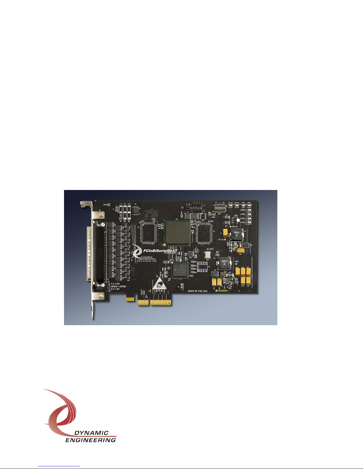
The PCIe compatible PCIeBiSerialDb37 has 18 independent differential IO available. A
DB-37 connector is mounted through the bezel to carry the signals. Each of the IO has
independent direction and termination controls. Each of the IO is matched length and
routed with 100 Ω differential impedance.
The IO’s are buffered from the FPGA with differential transceivers. The transceivers
can be populated with LVDS or RS-485 compatible devices. The power plane for the
transceivers is isolated to allow selectable 3.3 or 5V references for the IO. The LVDS
IO requires 3.3, and 40 MHz capable RS-485 requires 5V. When mixed LVDS and
RS485 are used the reference is set to 3.3 and lower speed [20 MHz] RS-485 parts are
used that are compatible with the 3.3V.
Each IO has pull-up and pull-down options to allow half duplex lines to be set to a
“marking” state when no device is on the line. The P is is ganged and the M side is too.
Each side can be set to GND or VCC to allow a ‘1’ or a ‘0’ to be set on the lines. The
resistors are in resistor packs and can be implemented with many values.
The terminations utilize analog switches to selectively parallel terminate the differential
pair with approximately 100 ohms. It is recommended that the receiver side provide the
termination.
The analog switches are protected with a diode on the input side of the power supply.
The switches can back-feed voltage into the rest of the circuit when powered down and
the system connected to it is not. The diodes allow for more flexible operation and
power sequencing.
PcieBiSerialDb37BA22 is a “clientized” version of the standard PCIeBiSerialDb37
Page 7

Embedded Solutions Page 7
board. “BA22” is set to use the LVDS standard, and supports one Transmit and one
Receive channel. The transmitter and receiver are designed to interface with a 2 bit
serial data stream with reference sync and clk. The base frequency is 73.636 MHz.
The transmit frequency is programmable using the A output from the PLL.
The receive side auto-bauds to the incoming rate. The data is deserialized and when
the synchronization pattern indicates, captured into a FIFO. The captured data is
available for DMA transfer to the host memory.
The Transmitter is supported with a combination of discrete 128Kx32 and BRAM based
FIFO’s for a total of 268,285 x 32 FIFO. Using DMA transfers the transmit side can
provide a continuous flow of data at the output. The transmitter has a programmable
frame start reference as well as programmable Line, Idle, Frame, Sync and PreAmble
lengths. In addition the control pattern for IDLEs, DATA, SYNC, and PreAmble are
programmable. The rate of transmission, and the dimensions of the transmission are
programmable.
Since the data is serialized as 2 -7 bit streams from 1 -14 bit word data is packed 2
pixels per LW. With the standard transmission rate of 73.636 MHz the effective unload
rate is (73.636/7)*2 or 5.259 MLW/S. The input side capability with DMA is 33 MLW/S
before overhead and perhaps 20 MLW/S with overhead.
The transmitter has an additional programmable feature of a minimum FIFO count
before starting transmission. By setting the count to be fairly large, the FIFO can be
effectively used as a timing buffer to insure a constant flow of data . With the large
multiplier (DMA vs Transmission) the “fill side” will always be able to keep up with the
transmitter on an overall basis. The FIFO will insure short term delays in processing do
not cause under-run issues. 268,285 x 2 * 3/4 * 7 * 13.58 => 38 mS of storage. [total
TX FIFO (LW) * 2 Pixels/LW * fraction filled when OS system delay happens* effective
bits per pixel [14 but 2 streams] * period of transmission clock]
The Receiver and Transmitter are separately supported with scatter gather capable
DMA engines.
Page 8
Embedded Solutions Page 8
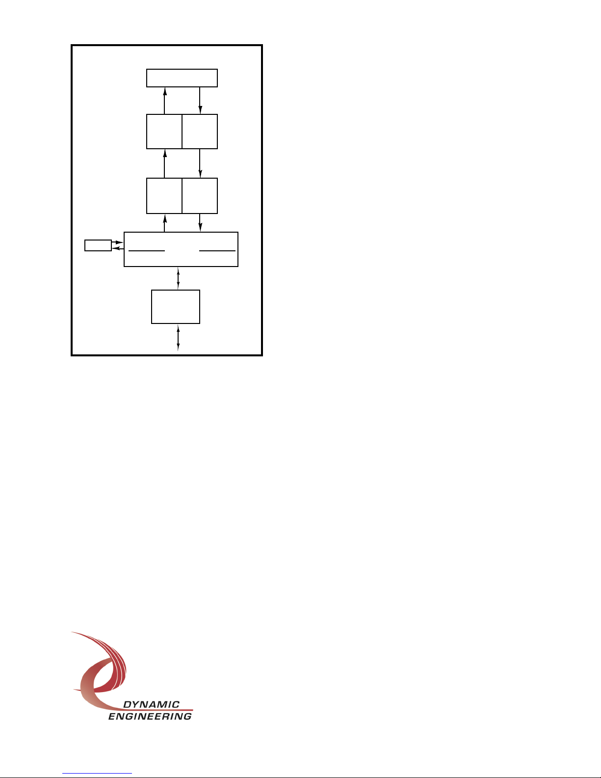
Figure 1 PcieBiSerialDb37BA22 Block Diagram
BA22 supports transmission and reception of serialized 2 bit wide data. The Data
transfer is controlled with a continuous clock plus sync pattern. The transmitter uses
the rising edge of the clock. The receiver uses the falling edge of the clock. The
serialized data is deserialized and stored as pixels, two per LW. The upper two bits per
stored pixel are used to mark frames and lines to allow for SW synchronization.
The PLL can be used to create a Tx clock reference. The control is via SW. The PLL is
referenced to 25 MHz. and can be programmed with new .JED files using the driver.
The hardware supports programming the PLL with an I2C bus , 2-256x32 FIFO’s and a
state-machine. The UserAp and driver provide a reference for programming the PLL.
The .JED file is the output from the Cypress 22393 programming tool. The Dynamic
Engineering SW “cracks” the .JED and loads the appropriate portions into the storage
elements for the state-machine to transfer to the PLL.
The transmitter hardware waits until the SW enable is set, the programmed minimum
data in the TX FIFO has been met, and the sync pulse is received [from the local timer].
Once in transmission the sync pulse and a non empty FIFO are the requirements to
(2 x 4 x LVDS)
termination
PCI IF
Data Flow
Control
PLL
TX FIFO
~262K x 32
TX State
Machine
RX FIFO
5K x 32
RX State
Machine
BA22
PCIe x4
PCI
Bridge
Page 9

Embedded Solutions Page 9
start sending the second, third…. frames. Once started if the data FIFO is empty when
the transmitter is ready to read the next data set, an error for underflow is flagged. The
error can cause an interrupt if desired.
An additional feature is programmable IDLE pattern output. When IDLEs are enabled in
the control register the transmitter will begin transmitting IDLEs whenever the statemachine is enabled. When IDLEs are not enabled, IDLEs are still transmitted between
lines and frames, but not when the transmitter is not active.
The receiver uses the received clock to capture data with a small state-machine that
loads the data into 2 parallel shift registers. Data from the shift registers is combined to
form pixels. In addition the upper bit [D15] is set when a frame boundary is
encountered. D14 is set for each line received. Frame detection is based on either the
Sync or PreAmble patterns being detected – next data pixel is then marked. Lines are
marked when Idles are detected, again on the next data pixel. If the IDLE pattern is the
same as the SYNC pattern all lines will be marked as having both Frame and Line.
Two pixels are stored to make a 32 bit quantity before moving to the first storage FIFO.
The reference rate of the input to the FIFO is the receive clock.
The read side of the first receive FIFO is tied to the input side of a 1Kx32 FIFO. The
second FIFO is used to support the receive DMA action.
The second FIFO has two sources. The transmit data chain can be looped back from a
point between the second discrete FIFO and the final transmission FIFO to the DMA
FIFO. With the Bypass bit set data loaded into the TX side can be read from the RX
side for an internal BIT. The first receive and last transmit stages are the only missing
pieces.
Both the transmitter and receiver allow for pixel reversal. The data is stored as 32 bit
words into the transmit FIFO from the system or the receive FIFO from the interface.
The pixel stored into the D15-0 or D31-16 can be transmitted first depending on the
selection of the transmit data order. Similarly the receive side data order can be
reversed if needed.
Custom cables can be manufactured to your requirements. The loop-back IO
definitions are toward the end of this manual. Please contact Dynamic Engineering with
your specifications.
In the “BA22” design the Termination and Direction controls are set in the VHDL for the
IO. The received signals are terminated and the transmitted signals are not.
All of the IO is routed through the FPGA to allow for custom applications. Larger
external and internal FIFO’s and Dual Ported memories are implemented for this
Page 10

Embedded Solutions Page 10
version by FPGA selection, and adding the 128K x 32 FIFO’s to the board.
The registers are mapped as 32 bit words and support 32 bit access. Most registers are
read-writeable. Windows® , Linux and other OS can be used to interface with this
design. For Dynamic Engineering drivers please check the DDS [Dynamic Data Sheet
on-line] . Custom drivers can be written for your situation. Existing drivers are “free” to
BA22 clients. Support programs are available based on the client’s level of expertise
and need. Use standard C/C++ to control your hardware or use the Hardware manual
to make your own software interface. The software manuals are also available on-line.
PcieBiserialDb37 can be used for multiple purposes with applications in
telecommunications, control, sensors, IO, test; anywhere multiple independent or
coordinated IO are useful.
PcieBiserialDb37 features a Xilinx FPGA, and high-speed differential devices. The
FPGA contains the PCI interface and control required for the IO interface.
The Xilinx design incorporates the “PCI Core” and additional modules for DMA in
parallel with a direct register decoded programming model. The design model has a
“base” level with the basic board level functions and “channels” which contain IO
oriented functions. In the BA22 design the IO functions are designed into the channel
and the PLL programming, switch, and other common or basic functions are in the base
design.
From a software perspective the design can be treated as “Flat” or as a hierarchy. The
Dynamic Engineering Windows® driver uses the hierarchical approach to allow for more
consistent software with common bit maps and offsets. This implementation has only
one channel. The channel function was kept to allow for future expansion with more
than 1 IO interface or a secondary function in added channels. The user software can
control the Channels with the same calls and use the channel number to distinguish.
This makes for consistent and easier to implement user level software.
The hardware is designed with each of the channels on a common address map – each
channel has the same memory allocated to it and as much as possible the offsets within
each space are defined in the same way or similar way. Again this make understanding
each port easier to accomplish and less likely to have errors.
The transceivers are initialized to the receive state. Once a channel is defined via
software to be a transmitter the IO are enabled and driven to the appropriate levels.
Terminations are activated for ports defined to be receivers.
PcieBiserialDb37 is part of the PCIe Module family of modular I/O components. The
PcieBiserialDb37 conforms to the PCIe standard. This guarantees compatibility with
your PCIe system. The base is 4 lane operation. The design can handle 1-4 lanes
Page 11
Embedded Solutions Page 11
being available. LED’s are provided to show the active PCIe lanes.
Designs implemented on PC104p, PMC, IP and PCIe versions of the BiSerial family can
in large part be ported between platforms. If you see what you need in one version and
prefer it on another please contact Dynamic Engineering about porting the design. In
most cases it will require a recompile of the VHDL and not much more. We do a lot of
“just like but different “ adaptations for our clients. Please contact us to help you with a
successful special adaptation of off- the-shelf hardware.
The DMA programmable length is 32 bits => longer than most computer OS will allow in
one segment of memory. The DMA is scatter gather capable for longer lengths than the
OS max and for OS situations where the memory is not contiguous. With Windows®
lengths of 4K are common while Linux can provide much larger spaces. Larger spaces
are more efficient as there are fewer initialization reads and reduced overhead on the
bus. A single interrupt can control the entire transfer. Head to tail operation can also be
programmed with two memory spaces with two interrupts per loop.
The hardware is organized with the IO function in channel 0 and the card level functions
in the “base”. The driver provides the ability to find the hardware and to allocate
resources to use the base and channel functions.
The basic use of the interface is to facilitate data transfer between the host and the
remote target.
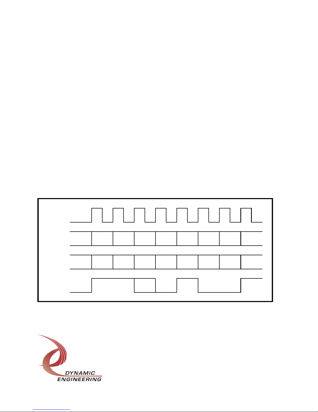
Figure 2 PCIEBISERIALDB37BA22 Timing Diagram
The clock is free running. The transmitter provides data with close to 50% duty cycle –
CLK
DATAL 6 5 4 3 2 1 0
DATAU 13 12 11 10 9 8 7
SYNC
F
6
13
Page 12
Embedded Solutions Page 12
changing on the rising edge, and stable on the falling edge.
The transmit rate is programmable for the BA22. PLL channel A is programmed to
73.636 MHz for a 73.636 MHz. output rate.
Sync programmable both for pattern and number of pixels. In addition a PreAmble is
provided again with programmable pattern and number of pixels. Master Frame Sync
=> PreAmble => Sync => Data/IDLE… complete Frame. If the number of PreAmble
Pixels is zero the HW will automatically skip to the Sync unless that is also zero pixels in
which case it starts with the Data Control pattern.
Some camera interfaces use a 1 pixel sync followed by some number of IDLE
characters to form a sync pattern. In this case the PreAmble is programmed as the
SYNC, the SYNC as the IDLE pattern and then DATA and IDLE as normal. The
PreAmble length would be 1 and the Sync length 3 or whatever the camera interface
requires.
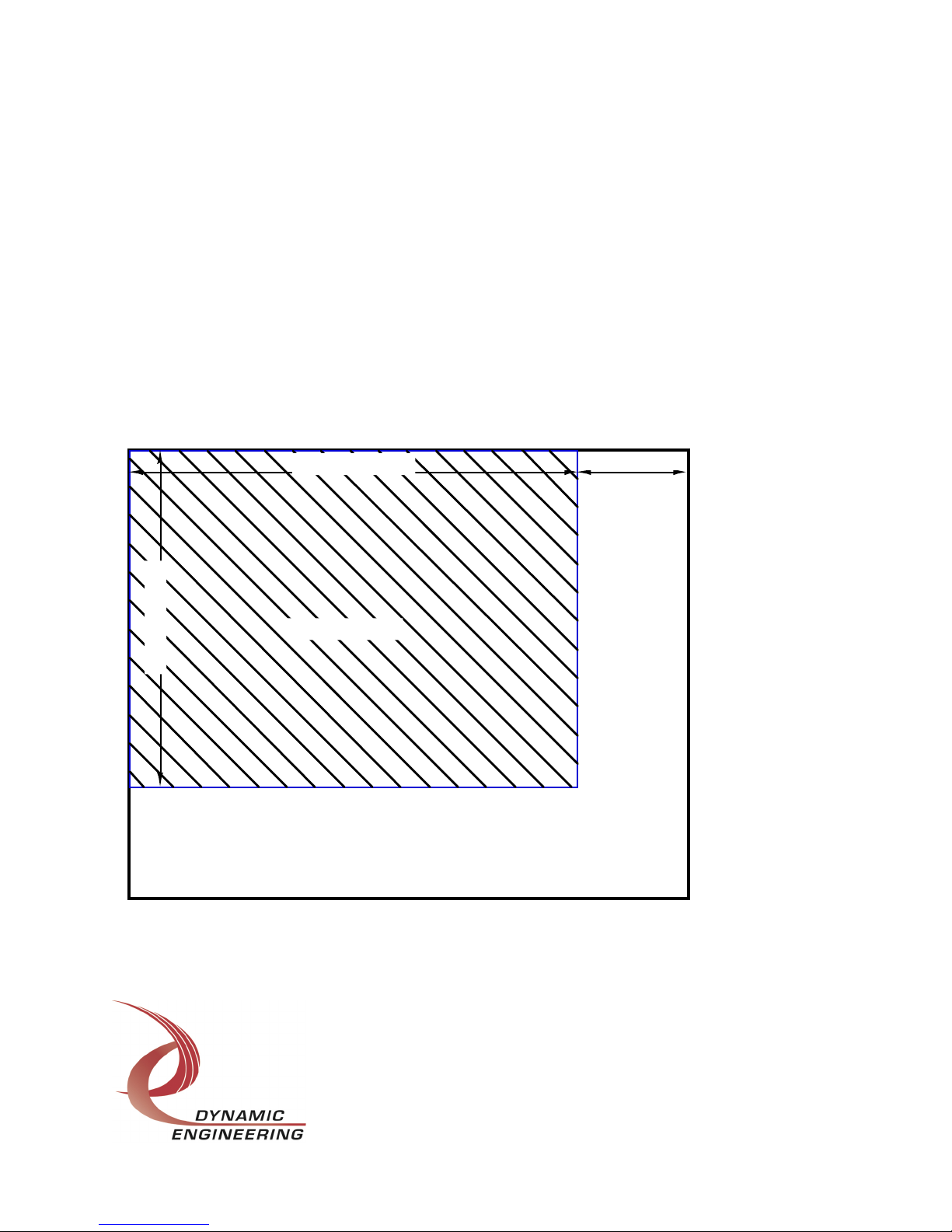
Figure 3 PCIEBISERIALDB37BA22 Image Diagram
The Image Transfer Area is controlled by programming the number of pixels per line
[Line Length], the number of pixel times at the end of a line [Idle Length], the number of
IDLE
IMAGE AREA
BLANKING
LINE LENGTH
LINE COUNT
Page 13

Embedded Solutions Page 13
lines per frame [Frame Length], and the repetition rate. The Blanking time is the
difference in the frame repetition rate and the size of the image and idle time. It is
programmed in terms of the reference rate clock. The time does not have to be an
integer number of pixels. Please see the register definitions for more detail.
Page 14

Embedded Solutions Page 14
Address Map
Base Address Map
Function Offset
// PCIeBiSerialDb37BA22 BASE definitions
#define BA22_BASE_BASE 0x0000 // 0 BA22Base Base control register
#define BA22_BASE_USER_SWITCH 0x0004 // 1 BA22Base User DIP switch read
#define BA22_BASE_XILINX_REV 0x0004 // 1 BA22Base Xilinx revision read port
#define BA22_BASE_XILINX_DES 0x0004 // 1 BA22Base Xilinx design read port
#define BA22_BASE_STATUS 0x0008 // 2 BA22Base status Register offset
#define BA22_BASE_PLL_WRITE 0x0000 // 4 BA22Base PLL FIFO write port
#define BA22_BASE_PLL_READ 0x0000 // 4 BA22Base PLL FIFO read port
Figure 4 PCIeBiSerialDb37BA22 Internal Address Map Base Functions
The address map provided is for the local decoding performed within
PcieBiserialDb37BA22. The addresses are all offsets from a base address. Dynamic
Engineering prefers a long-word oriented approach because it is more consistent across
platforms.
The map is presented with the #define style to allow cutting and pasting into many
compilers “include” files.
The host system will search the PCI bus to find the assets installed during power-on
initialization. The VendorId = 0xDCBA and the CardId = 0x0052 for the
PcieBiSerialDb37BA22.
The BA22 design has 1 channel implemented at this time. The BASE contains the
common elements of the design, while the Channels have the IO specific interfaces.
The BASE starts at the card offset. Channel 0 starts at register 20
Section Register Address Range COM name
(starting Hex address)
Base 0-19 (0x0000) PLL, Switch, Status
Channel 0 20-39 (0x0050) BA22 Transmitter & Receiver
Page 15

Embedded Solutions Page 15
Channel Address Map
Function Offset from Channel Base Address
#define CHAN_CNTRL 0x00000000 // 0 General control register
#define CHAN_STATUS 0x00000004 // 1 Interrupt status port
#define CHAN_INT_CLEAR 0x00000004 // 1 Interrupt clear port
#define CHAN_WR_DMA_PNTR 0x00000008 // 2 Write DMA dpr physical PCI address register
#define CHAN_TX_FIFO_COUNT 0x00000008 // 2 Tx FIFO count read port
#define CHAN_RD_DMA_PNTR 0x0000000C // 3 Read DMA dpr physical PCI address register
#define CHAN_RX_FIFO_COUNT 0x0000000C // 3 Rx FIFO count read port
#define CHAN_FIFO 0x00000010 // 4 FIFO offset for single word access R/W
#define CHAN_TX_AMT 0x00000014 // 5 Tx almost empty count register - used for Urgent
and pulsed interrupt
#define CHAN_RX_AFL 0x00000018 // 6 Rx almost full count register
#define CHAN_READY_CNT 0x00000024 // 9 Amount of data in pipeline before Tx can start
#define CHAN_FRAME_REF 0x00000028 // 10 Count representing time between frame start
triggers
#define CHAN_LINE_LENGTH 0x0000002C // 11 Number of pixels in a line
#define CHAN_IDLE_LENGTH 0x00000030 // 12 Number of idles at end of line
#define CHAN_FRAME_LENGTH 0x00000034 // 13 Number of lines in a frame
#define CHAN_TX_PreAmblePat 0x00000038 // 14 PreAmble Control Word
#define CHAN_TX_PreAmbleLen 0x0000003C // 15 PreAmble number of Pixels
#define CHAN_TX_SyncPat 0x00000040 // 16 Sync Control Word
#define CHAN_TX_SyncLen 0x00000044 // 17 Sync Number of Pixels
#define CHAN_TX_IdlePat 0x00000048 // 18 Idle Control Word
#define CHAN_TX_DataPat 0x0000004C // 19 Data Control Word
Figure 5 PcieBiSerialDb37BA22 Channel Address Map
Page 16

Embedded Solutions Page 16
Programming
Programming the PcieBiSerialDb37BA22 requires only the ability to read and write data
in the host's PCIe space.
Once the initialization process has occurred, and the system has assigned addresses to
the PcieBiSerialDb37BA22 card the software will need to determine what the address
space is for the PCI interface [BAR0]. The offsets in the address tables are relative to
the system assigned BAR0 base address.
The next step is to initialize the PcieBiSerialDb37BA22. The PLL will need to be
programmed to use the loop-back function or to transmit in the system. The Cypress
CyberClocks software can be used to create new .JED files if desired. PLLA should be
set to the transmit reference frequency output by the transmitter.
The driver comes with a .JED file prepared. The driver has a utility to load the PLL and
read back. The reference application software has an example of the use of PLL
programming. The reference application software also includes XLATE.c which
converts the .JED file from the CyberClocks tool to an array that can be programmed
into the PLL.
The IO for the BA22 direction and termination are hardwired in this design. The ports
are unidirectional and initialization is simplified with this approach.
The control bits for the BA22 will select how the data is transmitted – ordering, size of
transfer etc.
For Windows XP™ systems the Dynamic Driver can be used. The driver will take care
of finding the hardware and provide an easy to use mechanism to program the
hardware. The Driver comes with reference software showing how to use the card and
reference frequency files to allow the user to duplicate the test set-up used in
manufacturing at Dynamic Engineering. Using simple, known to work routines is a good
way to get acquainted with new hardware.
To use the BA22 specific functions the Channel Control, and PLL interface plus DMA
will need to be programmed. To use DMA, memory space from the system should be
allocated and the link list stored into memory. The location of the link list is written to
the BA22 to start the DMA. Please refer to the Burst IN and Burst Out register
discussions.
DMA should be set-up before starting the channel port function. For transmission this
will result in the FIFO being full or close to it when the transfer is started or at least the
Page 17

Embedded Solutions Page 17
Packet loaded if shorter than the FIFO size. For reception it means that the FIFO is
under HW control and the delay from starting reception to starting DMA won’t cause an
overflow condition.
DMA can be programmed with a specific length. The length can be as long as you want
within standard memory limitations. At the end of the DMA transfer the Host will receive
an interrupt. The Transmitter can be stopped, and the FIFO reset to clear out any
untransmitted data. For on-the-fly processing multiple shorter DMA segments can be
programmed; at the interrupt restart DMA to point at the alternate segment to allow
processing on the previous one. This technique is sometimes referred to as “pingpong”.
Please see the channel control register bit maps for more information.
Page 18

Embedded Solutions Page 18
Base Register Definitions
BA22_BASE_BASE
[$00 Base Control Register Port read/write]
DATA BIT DESCRIPTION
31-2 spare
1 ClrPll
0 PllProgEn
Figure 6 PcieBiSerialDb37BA22 Control Base Register Bit Map
This is the base control register for the BA22. The features common to all channels are
controlled from this port. Unused bits are reserved for additional new features. Unused
bits should be programmed ‘0’ to allow for future commonality.
PllProgEn: When this bit is set to a one, the state-machine used to program the PLL is
enabled to operate.
ClrPll: when set the PLL and associated memories are cleared. Must be returned to
cleared for normal operation.
The PLL is programmed with the output file generated by the Cypress PLL
programming tool. [CY3672 R3.01 Programming Kit or CyberClocks R3.20.00 Cypress
may update the revision from time to time.] The .JED file is used by the Dynamic Driver
to program the PLL. Programming the PLL is fairly involved and beyond the scope of
this manual. For clients writing their own drivers it is suggested to get the Engineering
Kit for this board including software, and to use the translation and programming files
ported to your environment. This procedure will save you a lot of time. For those who
want to do it themselves the Cypress PLL in use is the 22393. The output file from the
Cypress tool can be passed directly to the Dynamic Driver [Linux or Windows] and used
to program the PLL without user intervention.
The reference frequency for the PLL is 25 MHz.
Page 19

Embedded Solutions Page 19
BA22_BASE_ID
[$04 Switch and Design number port read only]
DATA BIT DESCRIPTION
31-24 spare
23-8 Design ID and Revision
7-0 DIP switch
Figure 7 PcieBiSerialDb37BA22 ID and Switch Bit Map
The DIP Switch is labeled for bit number, and ‘1’ ‘0’ in the silk screen. The DIP Switch
can be read from this port and used to determine which PcieBiserialDb37BA22 physical
card matches each PCI address assigned in a system with multiple cards installed.
The DIPswitch can also be used for other purposes – software revision etc. The switch
shown would read back 0x12.
The Design ID and Revision are defined by a 16 bit field allowing for 256 designs and
256 revisions of each. The BA22 design is 0x03 the current revision is 0x01.
The PCI revision is updated in HW to match the design revision. The board ID will be
updated for major changes to allow drivers to differentiate between revisions and
applications.
1
7 0
0
Page 20

Embedded Solutions Page 20
BA22_BASE_STATUS
[$08 Board level Status Port read only]
DATA BIT DESCRIPTION
31-19 set to ‘0
18-16 PllPckDnCnt
15-13 set to ‘0’
12 PllNakLat
11 PllPacketDoneLat
10 PllRdFifoMt
9 PllWrFifoMt
8 Pll Idle
7-1 set to ‘0’, reserved for additional channels
0 Unmasked Ch0 Interrupt
Figure 8 PcieBiSerialDb37BA22 Status Port Bit Map
Channel Interrupt – The local interrupt status from the channel. Each channel can have
different interrupt sources. DMA Write or DMA Read or IntForce or TX/RX request are
typical sources. Polling can be accomplished using the channel status register and
leaving the channel interrupt disabled.
Pll Idle when set indicates the PLL State-Machine is in the IDLE state.
PllWrFifoMt when set indicates the FIFO associated with writing data to the PLL is
empty. When cleared at least 1 location is filled.
PllRdFifoMt when set indicates the FIFO associated with reading data from the PLL is
empty. When cleared at least 1 location is filled.
PllPacketDoneLat is set and held when the PLL completes an operation. For example a
write to the PLL when completed will set this bit. This is a sticky bit. Cleared by writing
to the same address with this bit set.
PllNakLat when set indicates an operation to the PLL was not acknowledged. Usually
this is due to an improper address being used to communicate with the PLL. This is a
sticky bit. Clear by writing back with this bit position set.
PllPckDnCnt is a 3 bit count indicating how many operations have completed. Each
write operation takes 1 and each read takes 2 since the address is first written and then
the data read. The count can be used as a condition to know when a transfer is
completed. Count is cleared when the PllPacketDoneLat bit is cleared.
Page 21

Embedded Solutions Page 21
BA22_BASE_PLL_WRITE
BA22_BASE_PLL_READ
[$10 Board level PLL FIFO Port]
DATA BIT DESCRIPTION
31-0 LW written to / read from PLL
Figure 9 PcieBiSerialDb37BA22 PLL FIFO Port Bit Map
The transmit FIFO is monitored by the PLL state-machine. When the FIFO is written to
the first word is read by the state-machine and parsed. The first word contains the
mode on bit 0, address on 7-1, length on 15-8 [1-255], and the first byte or two to
transfer. If multiple bytes – 3 or more are to be transferred the SW will need to make
sure the data is in the FIFO for the 2nd LW before the end of the processing of the 2nd
byte or an underflow condition will be detected. If your system timing is tough to
manage it is suggested to disable the SM, load the FIFO and then enable the SM. A
status bit for the idle condition is available to allow SW to know when the SM has
responded to the disable.
The Length is the number of bytes in the data portion of the message + 1.
Please note: The PLL’s have two data sets written to two address offsets per PLL
programmed. The UserAp automatically converts the .jed file from the Cypress tool
and generates the local buffers with the hex data to load to the PLL. The application
software loads the FIFO with the correct address, length and data x2 for a complete
programming operation.
The State-machine will parse the message and write or read based on bit 0. In either
case the address and R/W are transmitted. An ACK is looked for from the Target. If a
Write the data is then transmitted with the ACK being checked after each byte.
Clocking is continuous until the message is completed. If a read is implemented, clocks
are generated without data after the address. Data is captured during the high portion
of the clock cycle, and the Master asserts the ACK until the last byte where a NAK is
asserted. Data is stored into the receive FIFO in this case.
The reference software has examples of working with the PLL’s and controlling HW.
Page 22

Embedded Solutions Page 22
Channel Bit Maps
The BA22 design has 1 channel. The basic control signals are the same for the
channel base, channel status, FIFO and DMA interfaces across multiple designs.
Notes:
The offsets shown are relative to the channel base address not the card base address.
BA22_CHAN_CNTRL
[0x0] Channel Control Register (read/write)
Channel Control Register
Data Bit Description
31-25 spare
24 TxInitialIdle
23 spare
22 RxDataOrder
21 CaptureAll
20 RxStart
19 RxOflInt
18 TxFrameCntLd
17 TxFrameCntEn
16 TxDataOrder
15 TxUflInt
14 TxFifoAmtInt
13 TxInt
12 TxStart
11-10 spare
9 External FIFO Reset
8 OutUrgent
7 InUrgent
6 Read DMA Interrupt Enable
5 Write DMA Interrupt Enable
4 Force Interrupt
3 Channel Interrupt Enable
2 Bypass
1 Receive FIFO Reset
0 Transmit FIFO Reset
Figure 10 PcieBiSerialDb37BA22 Channel Control Register
Page 23

Embedded Solutions Page 23
FIFO Transmitter/Receiver Reset: When set to a one, the transmit and/or receive FIFOs
will be reset. When these bits are zero, normal FIFO operation is enabled. In addition
the Transmit and Receive State Machines are also reset.
Write/Read DMA Interrupt Enable: These two bits, when set to one, enable the
interrupts for DMA writes and reads respectively.
Channel Interrupt Enable: When this bit is set to a one, all enabled interrupts (except
the DMA interrupts) will be gated through to the PCI interface level of the design; when
this bit is a zero, the interrupts can be used for status without interrupting the host. The
channel interrupt enable is for the channel level interrupt sources only.
Force Interrupt: When this bit is set to a one, a system interrupt will occur provided the
Channel Interrupt enable is set. This is useful for interrupt testing.
InUrgent / OutUrgent when set causes the DMA request to have higher priority under
certain circumstances. Basically when the TX FIFO is almost empty and InUrgent is set
the TX DMA will have higher priority than it would otherwise get. Similarly if the RX
FIFO is almost full and OutUrgent is set the read DMA will have higher priority. The
purpose is to allow software some control over how DMA requests are processed and to
allow for a higher rate channel to have a higher priority over other lower rate channels.
ByPass when set allows the FIFO to be used in a loop-back mode internal to the device.
A separate state-machine is enabled when ByPass is set and the TX and RX are not
enabled. The state-machine checks the TX and RX FIFO’s and when not empty on the
TX side and not Full on the RX side moves data between them. Writing to the TX FIFO
allows reading back from the RX side. An example of this is included in the Driver
reference software.
FIFO External Reset: When set to ‘1’, the External FIFO’s will be reset. When cleared
the External FIFO is enabled.
TxStart when set to ‘1’ provides the SW enable to the Tx state-machine to begin data
transfer. The state-machine waits for the combination of SW enable, Data Ready, and
Sync Pulse. Data Ready occurs when the Tx FIFO chain has enough data loaded.
The Sync Pulse re-occurs on the basis programmed with SW. Please see the other
register definitions for more detail. When disabled the state-machine will return to the
Idle state. The state-machine will complete the current task before returning. Reset
can be used to abort if the SW wants to force back to the Idle state.
TxInt when set to ‘1’ enables the transmitter to cause an interrupt for each frame
completed. Depending on the system this can provide a heartbeat, trigger more data to
be loaded etc.
Page 24

Embedded Solutions Page 24
TxFifoAmtInt when set enables the programmable interrupt based on the Transmit FIFO
level. Set the level to provide enough time to load more data. Since a programmed
level the amount of room [minimum] is already known. Alternatively use DMA for
automatic data transfer.
TxUflInt when set enables the Transmitter UnderFlow interrupt. If the last stage FIFO
is ever empty when the State-Machine needs another data point this status bit is set. If
this bit is enabled the status becomes an interrupt.
TxDataOrder, RxDataOrder can be used to swap the pixel order within each LW. On a
Windows system setting the bit will cause the lower pixel to be transmitted/received first.
X76543210 comes out x3210 x7654. Since endianness is affected by the CPU and the
OS and the driver you may need to experiment to get the data into the order you prefer.
Please note in the example, the “7” would be clipped since 14 bits of the 16 are actually
transmitted. The “3” would be ok since both of the upper bits are 0’s.
TxFrameCntEn when set allows the synchronization counter to run. The counter runs
from 0 to the programmed end count and repeats. A pulse is output at the end of each
counting cycle. TxFrameCntLd loads the Counter to a fixed value of 0x00 [basically a
clear in our application]. If the counter is disabled and a standard time base for restart
is required the counter should be cleared before being re-enabled.
RxOflInt when set enables the Receiver OverFlow Interrupt. If the Receiver FIFO is full
when it is time to load another LW the status is set. If the interrupt is enabled the
status becomes and interrupt request.
RxStart when set enables the receiver to capture data. Data is received, deserialized
and loaded into the receive FIFO. In standard operation the receiver waits for frame
sync to start capture.
CaptureAll when set causes the Receiver to capture all sync patterns and not wait for
frame sync to occur.
TxInitialIdle : Tx Initial Idle when set ‘1’ will cause the transmitter to use the IDLE
pattern to broadcast as soon as the transmitter is enabled. When not transmitting data
IDLEs are sent. When cleared, the IDLE pattern is only sent during “live”
transmissions. Not sent until the first frame is sent and stop once last frame is sent.
Page 25

Embedded Solutions Page 25
BA22_CHAN_STATUS
[0x4] Channel Status Read/Clear Latch Write Port
Channel Status Register
Data Bit Description
31 Interrupt Status
30 LocalInt
29 Transmitter Idle
28-27 spare
26 Tx DMA FIFO AFL
25 Tx DMA FIFO AMT
24 spare
23 BurstInIdle
22 BurstOutIdle
21 Ext FIFO 1 FULL
20 Ext FIFO 0 FULL
19 spare
18 RxFifoOvFlLat
17 TxFifoUnFlLat
16 TX FRAME DONE LAT
15 Read DMA Interrupt Occurred
14 Write DMA Interrupt Occurred
13 Read DMA Error Occurred
12 Write DMA Error Occurred
11 RxAFLvlIntLat
10 TxAELvlIntLat
9 EXT FIFO 1 MT
8 EXT FIFO 0 MT
7 spare
6 Rx FIFO Full
5 Rx FIFO Almost Full – complete chain
4 Rx FIFO Empty
3 Spare
2 Tx FIFO Full
1 Tx FIFO Almost Empty – complete chain
0 Tx FIFO Empty
Figure 11 PcieBiSerialDb37BA22 Channel STATUS PORT
BA22 FIFO: A 4K x 32 FIFO’s and a 1Kx32 FIFO are used to create the internal Rx
memory. The Tx side uses a combination of internal block RAM FIFO and two discrete
128Kx32 FIFO’s. The status for the Tx FIFO and Rx FIFO refer to these FIFO’s. The
Page 26

Embedded Solutions Page 26
status is active high. The Full and Empty status come from the “DMA” FIFO’s while
the Almost Full and Almost Empty status reflects the state of the total FIFO. 0x13 would
correspond to empty Rx and empty Tx DMA FIFO’s. The DMA FIFO’s are the pair of
internal FIFO’s which interact with the DMA engine. First in pipeline for TX and last in
pipeline for RX.
Please note with the Rx side status; the status reflects the state of the FIFO and does
not take the 4 deep pipeline into account. For example the FIFO may be empty and
there may be valid data within the pipeline. The data count with the combined FIFO and
pipeline value and can also be used for read size control. [see later in register
descriptions]
Rx FIFO Empty: When a one is read, the FIFO contains no data; when a zero is read,
there is at least one data word in the FIFO.
Rx FIFO Almost Full: When a one is read, the number of data words in the data FIFO is
greater than the value written to the corresponding RX_AFL_LVL register; when a zero
is read, the FIFO level is <= that value.
Rx FIFO Full: When a one is read, the receive data FIFO is full; when a zero is read,
there is room for at least one more data-word in the FIFO. If the FIFO is full when time
to write received data to the FIFO an overflow error is declared.
Tx FIFO Empty: When a one is read, the FIFO contains no data; when a zero is read,
there is at least one data word in the FIFO. If the FIFO is empty when time to read
transmitted data from the FIFO an underflow error is declared.
Tx FIFO Almost Empty: When a one is read, the number of data words in the data FIFO
is less than the value written to the corresponding TX_AMT_LVL register; when a zero
is read, the FIFO level is >= that value.
Tx FIFO Full: When a one is read, the transmit data FIFO is full; when a zero is read,
there is room for at least one more data-word in the FIFO.
RxFifoOvFlLat: When a one is read, an error has been detected. This will occur if FIFO
is full when the loader function tries to write to it. A zero indicates that no error has
occurred. This bit is latched and can be cleared by writing back to the Status register
with a one in the appropriate bit position.
TxFifoUnFlLat: When a one is read, an error has been detected. This will occur if FIFO
is empty when the state machine tries to read from it. A zero indicates that no error
has occurred. This bit is latched and can be cleared by writing back to the Status
register with a one in the appropriate bit position.
Page 27

Embedded Solutions Page 27
Write/Read DMA Error Occurred: When a one is read, a write or read DMA error has
been detected. This will occur if there is a target or master abort or if the direction bit in
the next pointer of one of the chaining descriptors is incorrect. A zero indicates that no
write or read DMA error has occurred. These bits are latched and can be cleared by
writing back to the Status register with a one in the appropriate bit position.
Write/Read DMA Interrupt Occurred: When a one is read, a write/read DMA interrupt is
latched. This indicates that the scatter-gather list for the current write or read DMA has
completed, but the associated interrupt has yet to be processed. A zero indicates that
no write or read DMA interrupt is pending.
Tx IDLE is set when the state-machine is in the idle state. When lower clock rates are
used it may take a while to clean-up and return to the idle state. If SW has cleared the
start bit to terminate the data transfer; SW can use the IDLE bit to determine when the
HW has completed its task and returned.
BO and BI Idle are Burst Out and Burst In IDLE state status for the Receive and
Transmit DMA actions. The bits will be 1 when in the IDLE state and 0 when
processing a DMA. A new DMA should not be launched until the State machine is back
in the IDLE state. Please note that the direction implied in the name has to do with the
DMA direction – Burst data into the card for Transmit and burst data out of the card for
Receive.
Local Interrupt is the masked combined interrupt status for the channel not including
DMA. The status is before the master interrupt enable for the channel.
Interrupt Status is the combined Local Interrupt with DMA and the master interrupt
enable. If this bit is set this channel has a pending interrupt request.
EXT FIFO Empty: When a one is read, the discrete FIFO(s) contains no data, when a
zero is read, there is at least one word in the FIFO.
EXT FIFO Full: When a one is read, the discrete FIFO(s) is full; when a zero is read,
there is room for at least one more word in the FIFO.
Please note: the EXT FIFO’s have a separate reset bit to clear those devices. Since
there is a pipeline involved, the resets should be applied together for best results.
Transmitter Idle is set when the Transmit State-Machine is in the Idle state. The statemachine operates at the PLLA rate and may take a few states to return to Idle from a
disable condition. The Idle state can be used to determine when the State-machine is
ready to be recommanded.
TxAELvlIntLat: When set the Tx Data FIFO has become almost Empty based on the
Page 28

Embedded Solutions Page 28
programmed count. The software can do a looped write or use DMA to load the
programmed count amount of data to the storage FIFO. The signal is latched and can
be cleared via write back with this bit set. The signal can be used to generate an
interrupt if desired.
RxAFLvlIntLat: When set the Rx Data FIFO has become almost Full based on the
programmed count. The software can do a looped read or use DMA to unload the
programmed count amount of data to the system memory. The signal is latched and
can be cleared via write back with this bit set. The signal can be used to generate an
interrupt if desired.
TX FRAME DONE LAT: is set at the end of each frame completed. The bit is latched
and cleared by writing back to this bit position. If enabled this status can cause an
interrupt. The status and interrupt can be used for a heart-beat, trigger another DMA
transfer etc.
Page 29

Embedded Solutions Page 29
BA22_CHAN_WR_DMA_PNTR
[0x8] Write DMA Pointer (write only)
BurstIn DMA Pointer Address Register
Data Bit Description
31-2 First Chaining Descriptor Physical Address
1 direction [0]
0 end of chain
Figure 12 PcieBiSerialDb37BA22 Write DMA pointer register
This write-only port is used to initiate a scatter-gather write [TX] DMA. When the
address of the first chaining descriptor is written to this port, the DMA engine reads
three successive long words beginning at that address. Essentially this data acts like a
chaining descriptor value pointing to the next value in the chain.
The first is the address of the first memory block of the DMA buffer containing the data
to read into the device, the second is the length in bytes of that block, and the third is
the address of the next chaining descriptor in the list of buffer memory blocks. This
process is continued until the end-of-chain bit in one of the next pointer values read
indicates that it is the last chaining descriptor in the list.
All three values are on LW boundaries and are LW in size. Addresses for successive
parameters are incremented. The addresses are physical addresses the HW will use
on the PCI bus to access the Host memory for the next descriptor or to read the data to
be transmitted. In most OS you will need to convert from virtual to physical. The length
parameter is a number of bytes, and must be on a LW divisible number of bytes.
Status for the DMA activity can be found in the channel control register and channel
status register.
Notes:
1. Writing a zero to this port will abort a write DMA in progress.
2. End of chain should not be set for the address written to the DMA Pointer
Address Register. End of chain should be set when the descriptor follows the
last length parameter.
3. The Direction should be set to ‘0’ for Burst In DMA in all chaining descriptor
locations.
Page 30

Embedded Solutions Page 30
BA22_CHAN_TX_FIFO_COUNT
[0x8] TX [Target] FIFO data count (read only)
TX FIFO Data Count Port
Data Bit Description
31-0 TX Data Words Stored
Figure 13 PcieBiSerialDb37BA22 TX FIFO data count Port
This read-only register port reports the number of 32-bit data words in the Transmit
FIFO.
BA22_CHAN_RD_DMA_PNTR
[0xC] Read DMA Pointer (write only)
BurstIn DMA Pointer Address Register
Data Bit Description
31-2 First Chaining Descriptor Physical Address
1 direction [1]
0 end of chain
Figure 14 PcieBiSerialDb37BA22 Read DMA pointer register
This write-only port is used to initiate a scatter-gather read [RX] DMA. When the
address of the first chaining descriptor is written to this port, the DMA engine reads
three successive long words beginning at that address. Essentially this data acts like a
chaining descriptor value pointing to the next value in the chain.
The first is the address of the first memory block of the DMA buffer to write data from
the device to, the second is the length in bytes of that block, and the third is the address
of the next chaining descriptor in the list of buffer memory blocks. This process is
continued until the end-of-chain bit in one of the next pointer values read indicates that it
is the last chaining descriptor in the list.
All three values are on LW boundaries and are LW in size. Addresses for successive
parameters are incremented. The addresses are physical addresses the HW will use
on the PCI bus to access the Host memory for the next descriptor or to read the data to
be transmitted. In most OS you will need to convert from virtual to physical. The length
parameter is a number of bytes, and must be on a LW divisible number of bytes.
Status for the DMA activity can be found in the channel control register and channel
status register.
Page 31

Embedded Solutions Page 31
Notes:
1. Writing a zero to this port will abort a write DMA in progress.
2. End of chain should not be set for the address written to the DMA Pointer
Address Register. End of chain should be set when the descriptor follows the
last length parameter.
3. The Direction should be set to ‘1’ for Burst Out DMA in all chaining descriptor
locations.
BA22_CHAN_RX_FIFO_COUNT
[0xC] RX [Master] FIFO data count (read only)
RX FIFO Data Count Port
Data Bit Description
31-0 RX Data Words Stored
Figure 15 PcieBiSerialDb37BA22 RX FIFO data count Port
This read-only register port reports the number of 32-bit data words in the Receive FIFO
plus pipeline. The maximum count is the FIFO size plus 4.
BA22_CHAN_FIFO
[0x10] Write TX/Read RX FIFO Port
RX and TX FIFO Port
Data Bit Description
31-0 FIFO data word
Figure 16 PcieBiSerialDb37BA22 RX/TX FIFO Port
This port is used to make single-word accesses to and from the FIFO. Data read from
this port will no longer be available for DMA transfers. Writing to the port loads the Tx
FIFO, Reading unloads the Rx FIFO.
Two pixels are stored per LW. Pixels are 14 bits. Upper two bits per pixel for transmit
are ignored. Upper two bits per pixel for Rx are reserved.
D31,D30, D29-D16, D15, D14 D13-0 The data transmitted and received for the D29-16
and D13-0 can be reversed orderwise to match your system memory situation. See the
Data_Order control bits. The receive data has an extra feature. Bit 15/31 is set for the
pixel corresponding to one having the frame bit set.
Page 32

Embedded Solutions Page 32
BA22_CHAN_TX_AMT_LVL
[0x14] Tx almost-empty level (read/write)
Tx Almost-Full Level Register
Data Bit Description
31-0 Tx FIFO Almost-Empty Level
Figure 17 PcieBiSerialDb37BA22 TX ALMOST EMPTY LEVEL register
This read/write port accesses the almost-empty level register. When the number of
data words in the transmit data FIFO is less than this value, the almost-empty status bit
will be set. The register is R/W for 32 bits. The mask is valid for a size matching the
depth of the FIFO.
BA22_CHAN_RX_AFL_LVL
[0x18] Rx almost-full (read/write)
Rx Almost-Full Level Register
Data Bit Description
31-0 Rx FIFO Almost-Full Level
Figure 18 PcieBiSerialDb37BA22 RX ALMOST FULL LEVEL register
This read/write port accesses the almost-full level register. When the number of data
words in the receive data FIFO is equal or greater than this value, the almost-full status
bit will be set. The mask is valid for a size matching the depth of the FIFO. The level
includes the pipeline for an additional 4 locations.
Page 33

Embedded Solutions Page 33
BA22_CHAN_READY_CNT
[0x24] Tx Ready Count(read/write)
Tx Ready Count Register
Data Bit Description
31-0 Amount of data required to start transmission
Figure 19 PcieBiSerialDb37BA22 TX Ready Count Register
This read/write port accesses the Ready Count register. When the number of data
words in the transmit data FIFO is greater or equal to this value, the FIFO READY
signal to the TX State Machine will be set.
BA22_CHAN_FRAME_REF
[0x28] Tx Frame Ref(read/write)
Tx Frame Period Register
Data Bit Description
31-0 Set Frame Period
Figure 20 PcieBiSerialDb37BA22 TX Frame Reference Register
This read/write port accesses the Frame Reference register. PLLA clock is the time
base. 73.636 MHz for BA22. This corresponds to 13.58 nS per period. The Frame
repetition rate is the number set in the reference * the period. Please note: There is a
SW hazard if the frame period is set shorter than the transmission time of the
programmed frame. The State Machine will send the programmed frame and then wait
for the next Frame Start pulse [comes at the start of each programmed frame time]. If
the value is programmed too small / too much data the HW will miss the frame start and
wait for the next one.
Also the period is in terms of the clock rather than pixels so it is possible to create
frames that are on pixel time or something non-integer.
Page 34

Embedded Solutions Page 34
BA22_CHAN_LINE_LENGTH
[0x2C] Tx Line Length(read/write)
Tx Line Length Register
Data Bit Description
31-0 Amount of data required to start transmission
Figure 21 PcieBiSerialDb37BA22 TX Line Length Register
This read/write port accesses the Line Length register. Set the number of pixels per line
to be transmitted with this register. For each pixel, 7 clock periods will be used to
transmit the 14 bits.
BA22_CHAN_IDLE_LENGTH
[0x30] Tx Idle Length(read/write)
Tx Idle Length Register
Data Bit Description
31-0 Amount of data required to start transmission
Figure 22 PcieBiSerialDb37BA22 TX Idle Length Register
This read/write port accesses the Idle Length register. Set the number of pixels times
per line to be transmitted with this register. For each pixel, 7 clock periods will be used
to transmit the 14 bits. Data is set to ‘0’ for each bit location and the sync is also set to
the IDLE pattern [all ‘0’].
Page 35

Embedded Solutions Page 35
BA22_CHAN_FRAME_LENGTH
[0x34] Tx Frame Length(read/write)
Tx Frame Length Register
Data Bit Description
31-0 Amount of data required to start transmission
Figure 23 PcieBiSerialDb37BA22 TX Frame Length Register
This read/write port accesses the Frame Length register. Set the number of Lines per
Frame to be transmitted with this register.
(Line Length + Idle Length) * 7 * Frame Length = the period in clocks for the transmitted
portion of the Frame. The FRAME REF is also in clocks and should be larger than this
number for standard operation.
CHAN_TX_PreAmblePat
[0x38] Tx PreAmble (read/write)
Tx PreAmble Pattern Register
Data Bit Description
7-0 Control Pattern to send during PreAmble
Figure 24 PcieBiSerialDb37BA22 TX PreAmble Pattern Register
This read/write port accesses the PreAmble Pattern register. Set the control data to
send during PreAmble time. PreAmble will be sent when the Master Sync has been
detected for PreAmbleLen pixels. If programmed to 0 length the PreAmble is skipped.
CHAN_TX_PreAmbleLen
[0x3C] Tx PreAmble Length(read/write)
Tx PreAmble Length Register
Data Bit Description
15-0 Number of PreAmble pixels to send
Figure 25 PcieBiSerialDb37BA22 TX PreAmble Length Register
This read/write port accesses the PreAmble Length register. If programmed to 0 length
the PreAmble is skipped. If set to a non-zero length, that number of PreAmble pixels is
Page 36

Embedded Solutions Page 36
transmitted. Data is held as “00” during transmission.
CHAN_TX_SyncPat
[0x40] Tx Sync (read/write)
Tx Sync Pattern Register
Data Bit Description
7-0 Control Pattern to send during Sync
Figure 26 PcieBiSerialDb37BA22 TX Sync Pattern Register
This read/write port accesses the Sync Pattern register. Set the control data to send
during Sync time. Sync will be sent when the Master Sync has been detected for
SyncLen pixels. If programmed to 0 length the Sync is skipped.
CHAN_TX_SyncLen
[0x44] Tx Sync Length(read/write)
Tx Sync Length Register
Data Bit Description
15-0 Number of Sync pixels to send
Figure 27 PcieBiSerialDb37BA22 TX Sync Length Register
This read/write port accesses the Sync Length register. If programmed to 0 length the
Sync is skipped. If set to a non-zero length, that number of PreAmble pixels is
transmitted. Data is held as “00” during transmission.
CHAN_TX_IdlePat
[0x48] Tx Idle Pattern(read/write)
Tx IDLE Pattern Register
Data Bit Description
7-0 Control Pattern to send during IDLE
Figure 28 PcieBiSerialDb37BA22 TX Idle Pattern Register
This read/write port accesses the Idle Pattern register. Set the control data to send
Page 37

Embedded Solutions Page 37
during Idle time. Idle will be sent for the programmed length between lines [Idle Time]
and between frames as programmed with the difference in frame time and the master
sync period.
CHAN_TX_DataPat
[0x4C] Tx Data Pattern (read/write)
Tx Data Pattern Register
Data Bit Description
7-0 Control Pattern to send during Data
Figure 29 PcieBiSerialDb37BA22 TX Data Pattern Register
This read/write port accesses the Data Pattern register. Set the control data to send
during Data transmission time. The Data control word will be sent on the control line in
parallel with the transmitted data.
Page 38

Embedded Solutions Page 38
Loop-back
The Engineering kit includes reference software, utilizing external loop-back tests.
The test set-up included PcieBiSerialDb37BA22 and loop-back plug. The Pin numbers
are for the interconnections on the Loop-back plug. The IO names can be used to
accommodate a different set-up. The loop-back plug is a DB37 connector with the
interconnections protected with a connector shell. Twisted Pair wiring is used. For
short cables Cat5e can be used.
Signal From To Signal
TxPSync+ 1 5 RxPSync+
TxPSync- 2 6 RxPSyncTxPDataU+ 20 24 RxPDataU+
TxPDataU- 21 25 RxPDataUTxPDataL+ 3 7 RxPDataL+
TxPDataL- 4 8 RxPDataLTxPClk+ 22 26 RxPClk+
TxPClk- 23 27 RxPClk-
Figure 24 PcieBiSerialDb37BA22 Loop-Back wiring diagram
Page 39

Embedded Solutions Page 39
PCIe Module Front Panel IO Interface Pin Assignment
The figure below gives the pin assignments for the IO Interface on the
PcieBiSerialDb37BA22.
IO_0p (TxPSync+) IO_0m (TxSync-) 1 2
IO_1p (TxPDataU+) IO_1m (TxDataU-) 20 21
IO_2p (TxPDataL+) IO_2m (TxDataL-) 3 4
IO_3p (TxPClk+) IO_3m (TxClk-) 22 23
IO_4p (RxPSync+) IO_4m (RxPSync-) 5 6
IO_5p (RxPDataU+) IO_5m (RxPDataU-) 24 25
IO_6p (RxPDataL+) IO_6m (RxPDataL-) 7 8
IO_7p (RxPClk+) IO_7m (RxPClk-) 26 27
IO_8p (unused) IO_8m (unused) 9 10
IO_9p (unused) IO_9m (unused) 28 29
IO_10p (unused) IO_10m (unused) 11 12
IO_11p (unused) IO_11m (unused) 30 31
IO_12p (unused) IO_12m (unused) 13 14
IO_13p (unused) IO_13m (unused) 32 33
IO_14p (unused) IO_14m (unused) 15 16
IO_15p (unused) IO_15m (unused) 34 35
IO_16p (unused) IO_16m (unused) 17 18
IO_17p (unused) IO_17m (unused) 36 37
GND* 19
Figure 25 PcieBiSerialDb37BA22 FRONT PANEL Interface
GND is shunt selectable for DC, AC and open configurations. Jumper is located near
lower edge of DB37 connector. Options labeled in silk-screen
Page 40

Embedded Solutions Page 40
Applications Guide
Interfacing
The pin-out tables are displayed with the pins in the same relative order as the actual
connectors. Some general interfacing guidelines are presented below. Do not hesitate
to contact the factory if you need more assistance.
Watch the system grounds. All electrically connected equipment should have a fail-safe
common ground that is large enough to handle all current loads without affecting noise
immunity. Power supplies and power-consuming loads should all have their own ground
wires back to a common point.
Power all system power supplies from one switch. Differential interface devices provide
some immunity from, and allow operation when part of the circuit is powered on and
part is not. It is better to avoid the issue of going past the safe operating areas by
powering the equipment together and by having a good ground reference.
Keep cables short. Flat cables, even with alternate ground lines, are not suitable for
long distances. In addition series resistors are used and can be specified to be
something other than the 0 ohm standard value. The connector is pinned out for a
standard DB37 cable to be used. It is suggested that this standard cable be used for
most of the cable run or an equivalent with proper twisted pairs and shielding.
Coming Soon. Terminal Block. We offer a high quality 37 screw terminal block that
directly connects to the DB37. The terminal block can mount on standard DIN rails.
DBterm37 has an associated twisted pair cable compatible with the PCIeBiSerialDB37.
[ http://www.dyneng.com/DBterm68.html ]
We provide the components. You provide the system. Safety and reliability can be
achieved only by careful planning and practice. Inputs can be damaged by static
discharge, or by applying voltage outside of the particular device’s rated voltages.
Page 41

Embedded Solutions Page 41
Construction and Reliability
PCIe Modules were conceived and engineered for rugged industrial environments. The
PcieBiSerialDb37BA22 is constructed out of 0.062 inch thick high temperature ROHS
compliant material.
The traces are matched length from the FPGA ball to the IO pin. The analog switches
and termination resistors are located directly under the transceivers and connected with
“zero stub” routing to eliminate unwanted effects from unused options.
Surface mounted components are used. The components are available with
commercial and Industrial temperature ranges. Please order the “ET” version for more
demanding environments. Conformal coating is an option for condensing environments
or for another measure of board protection. Please order the “CC” version.
The PCIe is secured against the chassis with the connectors and front panel. If more
security against vibration is required a chassis with top side support can be used. The
PCIeBiSerialDb37 has a wider keep out than required by PCIe specification to allow use
in industrial chassis and horizontal mount situations.
The power and ground planes are implemented with relatively heavy copper to help with
heat spreading in chassis with limited air flow. The components are spaced to allow for
efficient cooling and power dispersion.
Thermal Considerations
The PcieBiSerialDb37BA22 design consists of CMOS and similar circuits. The power
dissipation due to internal circuitry is very low. It is possible to create higher power
dissipation with the externally connected logic. If more than one Watt is required to be
dissipated due to external loading; cooling with forced air is recommended. With the one
degree differential temperature to the solder side of the board external cooling is easily
accomplished.
Page 42

Embedded Solutions Page 42
Warranty and Repair
Please refer to the warranty page on our website for the current warranty offered and
options. http://www.dyneng.com/warranty.html
Service Policy
Before returning a product for repair, verify as well as possible that the suspected unit is
at fault. Then call the Customer Service Department for a RETURN MATERIAL
AUTHORIZATION (RMA) number. Carefully package the unit, in the original shipping
carton if this is available, and ship prepaid and insured with the RMA number clearly
written on the outside of the package. Include a return address and the telephone
number of a technical contact. For out-of-warranty repairs, a purchase order for repair
charges must accompany the return. Dynamic Engineering will not be responsible for
damages due to improper packaging of returned items. For service on Dynamic
Engineering Products not purchased directly from Dynamic Engineering contact your
reseller. Products returned to Dynamic Engineering for repair by other than the original
customer will be treated as out-of-warranty.
Out of Warranty Repairs
Out of warranty repairs will be billed on a material and labor basis. Customer approval
will be obtained before repairing any item if the repair charges will exceed one half of
the quantity one list price for that unit. Return transportation and insurance will be billed
as part of the repair and is in addition to the minimum charge.
For Service Contact:
Customer Service Department
Dynamic Engineering
150 DuBois St. Suite C
Santa Cruz, CA 95060
831-457-8891
831-457-4793 fax
support@dyneng.com
Page 43

Embedded Solutions Page 43
Specifications
Logic Interface: PCIe 1-4 lanes. 4 lanes recommended
Digital Parallel IO: LVDS IO
Digital Serial IO: 2 bit serial with sync and reference clock.. Data
valid on falling edge of clock. 76.636 MHz for initial
target design.
DIP Switch: DipSwitch supplied for board identification and
other user purposes.
CLK rates supported: PLLA is programmed to select Transmit Clock rate.
For loop-back and alternate HW implementations.
PLLB, C, D reserved for new applications.
Software Interface: Control Registers, IO registers, IO Read-Back
registers, FIFO. R/W, 32 bit boundaries.
Initialization: Programming procedure documented in this
manual
Access Modes: LW to registers, read-write to most registers
Access Time: Frame to TRDY 121 nS [4 PCI clocks] or burst
mode DMA – 1 word per PCI clock transferred.
Interrupt: Each port has independently programmable
interrupt sources, DMA interrupts included.
Onboard Options: All Options are Software Programmable
Interface Options: 37 Pin DB connector at front bezel.
Dimensions: Standard 1/2 length PCIe module.
Construction: Multi-Layer Printed Circuit, Through Hole and
Surface Mount Components.
Power: +12 and +3.3 used from PCIe interface. No
secondary power supply connections required. 1.2,
2.5 and 5V developed locally.
Weight: TBD oz
Page 44

Embedded Solutions Page 44
Order Information
standard temperature range Industrial
PcieBiSerialDb37BA22 PCIe Module with Transmitter and Receiver .
[2 bit serial image data plus sync and clock]
http://www.dyneng.com/pciebiserialdb37.html
Order Options:
Pick any combination to go with IO
-CC to add conformal coating
-ET to change to industrial Temp [-40 - +85C]
Dbterm37: 37 position terminal block with DB37
connector.
http://www.dyneng.com/DBterm37.html
Dbcabl37: DB37 cable compatible with
PCIeBiSerialDB37. Twisted pairs on correct
pin pairs.
http://www.dyneng.com/DBcabl37.html
PCIe BiSerial DB37 BA22 Eng Kit : Windows Driver software, Loop-Back Plug,
reference schematics. Recommended for first
time purchases.
http://www.dyneng.com/pciebiserialdb37.html
All information provided is Copyright Dynamic Engineering
 Loading...