

Page 1
DYNAMIC ENGINEERING
150 Dubois St. Suite C, Santa Cruz, CA 95060
831-457-8891 Fax 831-457-4793
http://www.dyneng.com
sales@dyneng.com
Est. 1988
User Manual
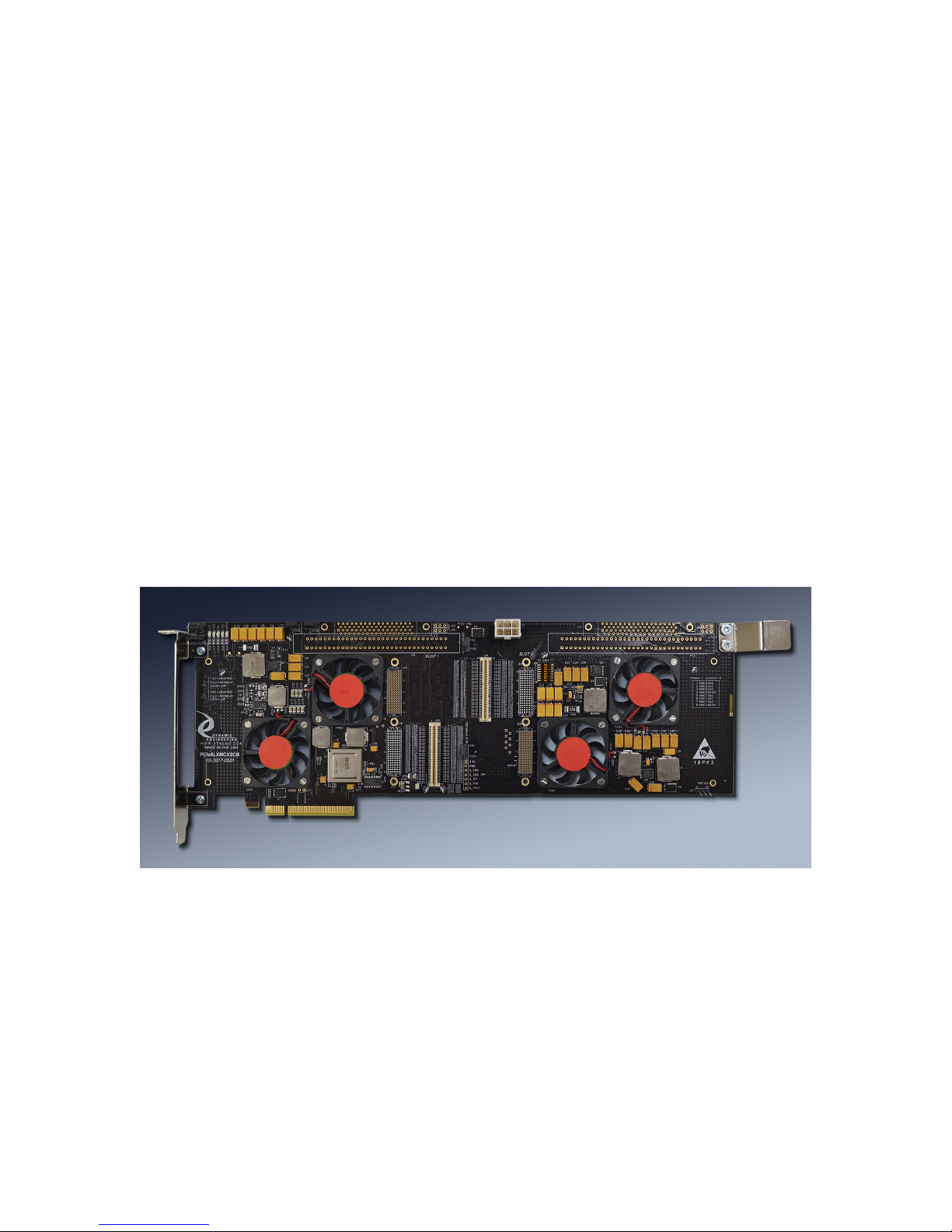
PCIe8LXMCX2CB
PCIe 8 Lane 2 Position XMC Compatible Carrier
Connector Bus Version
Shown With JN4 full CB, 4 fans installed, AP power connector
Revision A2 9/6/17
Corresponding Hardware: Revision A
Fab number 10-2017-0501
Page 2

Embedded Solutions Page 2
PCIe8LXMCX2CB
PCIe and XMC Compatible Carrier
Dynamic Engineering
150 Dubois St. Suite C
Santa Cruz, CA 95060
831457-8891
831457-4793 FAX
This document contains information of
proprietary interest to Dynamic Engineering. It
has been supplied in confidence and the
recipient, by accepting this material, agrees that
the subject matter will not be copied or
reproduced, in whole or in part, nor its contents
revealed in any manner or to any person except
to meet the purpose for which it was delivered.
Dynamic Engineering has made every effort to
ensure that this manual is accurate and
complete. Still, the company reserves the right
to make improvements or changes in the
product described in this document at any time
and without notice. Furthermore, Dynamic
Engineering assumes no liability arising out of
the application or use of the device described
herein.
The electronic equipment described herein
generates, uses, and can radiate radio
frequency energy. Operation of this equipment
in a residential area is likely to cause radio
interference, in which case the user, at his own
expense, will be required to take whatever
measures may be required to correct the
interference.
Dynamic Engineering’s products are not
authorized for use as critical components in life
support devices or systems without the express
written approval of the president of Dynamic
Engineering.
Connection of incompatible hardware is likely to
cause serious damage.
©2012-2017 by Dynamic Engineering.
Other trademarks and registered trademarks are owned by their
respective manufactures.
Page 3

Embedded Solutions Page 3
PRODUCT DESCRIPTION 4!
Headers and TestPoints 6!
DipSwitch Settings 7!
Options 8!
XMC Module Backplane IO Interface Pin Assignment 10!
XMC Module IO Resistor Selection 11!
XMC Module Connector Resistor Selection 13!
APPLICATIONS GUIDE 15!
Interfacing 15!
Construction and Reliability 16!
Thermal Considerations 16!
WARRANTY AND REPAIR 17!
Service Policy 17!
Out of Warranty Repairs 17!
For Service Contact: 17!
SPECIFICATIONS 18!
ORDER INFORMATION 19!
Table of Contents
Page 4

Embedded Solutions Page 4
FIGURE 1! PCIE8LXMCX2CB JN4/JN6 INTERFACE STANDARD 10!
FIGURE 2! PCIE8LXMCX2CB RESISTOR SELECTION IO 12!
FIGURE 3! PCIE8LXMCX2CB RESISTOR SELECTION CONNECTOR 14!
Product Description
PCIe8LXMCX2CB is part of the Dynamic Engineering PCIe and XMC Compatible family
of modular I/O components. PCIe8LXMCX2CB adapts 2 XMC’s to one PCIe slot.
Embedded applications frequently require real time processing coupled with special
purpose IO. With PCIe8LXMCX2CB’s two XMC positions; a PrXMC can be matched
with another XMC to make a high bandwidth processing node. The PrXMC can
communicate with the host for set-up, and then use the local bus to control and transfer
data with the special purpose IO card.
The CB model has a Connector Bus between the two XMC rear IO connectors. 0 ohm
resistors are used to select which lines are cross-connected and which go to the
standard IO options. The resistors are located front and back with almost “0” stub
length for the unused feature. The connections are impedance controlled and matched
length routed as differential pairs. 100 ohms.
A selection table is provided to help with resistor stuffing selection. Both of the
corresponding CB resistors will need to be installed to make the CB connection. For
example IO0_0P can be connected to IO1_0P by selection of both CB resistors for that
line. The standard IO connections will normally not be selected in this case, and can
be if it makes sense for your system.
Since there are 64 rear IO lines per XMC and each need 4 resistors; a total of 512
resistors are available. Too many to have a standardized table of options. Contact
Dynamic Engineering with your requirement. We will create a new -# to cover your
configuration. A small charge is required to cover the cost of an updated programming
file for the PnP and test program.
1st select which connector is tied to the IO. This can be on a signal by signal basis.
Either, neither, both. 2nd select which IO to connect the selected connections. See
List of Figures
Page 5
Embedded Solutions Page 5
figures 2 & 3 at the rear of this manual.
Install the RP/RX resistors to tie the XMC signal to the selection point – to distribute to
the SCSI or DIN connector and or other XMC position. Use RCB and/or RIO to select
the IO side of the connection. This “I” form made of 4 0402 resistors allows for selection
with almost no signal stub. Selectable on a signal by signal basis.
Special features:
• 24 lane Gen1/2 compliant Switch
• 8 lanes allocated to PCIe “gold finger” interface. 8 lanes each to the XMC’s
• Switch can store and forward locally to communicate directly between the XMC’s
• Voltage monitors, each with LED’s on plus 12V, minus 12V, plus 5V, plus 3.3V, and
switch power [1.0V]
• 10A regulator for XMC 3.3V and 5V supplies. Shunts for Delayed, not Delayed, Off
• Selection switch for VPWR [12V or 5V] per XMC. Option for hardwired 5V or 12V
• Front panel connector access through PCI bracket
• User IO [Jn4 and/or Jn6] available through one of two cable connectors (DIN IDC or
SCSI II compatible) Spare pins on SCSI connector can be shunt selected to power
or ground.
• Connector Bus available to cross connect XMC rear IO between modules
• Cooling cutout for increased airflow to XMC’s
• Optional Fan(s) for increased airflow
• JTAG programming support
• DIP switch to select global addressing on XMC’s
The PCIe8LXMCX2CB is ready to use with the default settings. Just install the XMC(s)
onto PCIe8LXMCX2CB and then into the system.
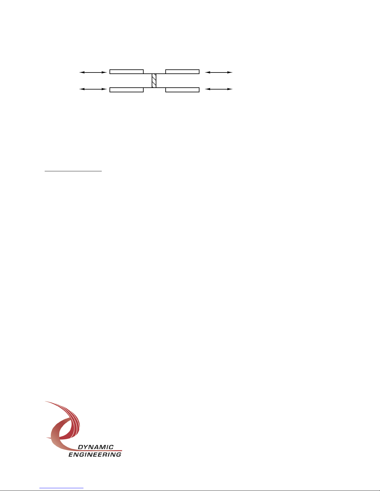
RP RX
RIO RCB
SCSI/DIN XMC
JN6
JN4
Page 6

Embedded Solutions Page 6
Headers and TestPoints
J6 and J11 are used to select the VPWR source for position 0 and 1 respectively.
When the Shunt closes 1-2 – 12V is selected. With 2-3 closed 5V is selected. FET’s
are used to provide a low impedance path from the power supplies to VPWR for each
position. Options are in place on the PCB to allow hardwired selections for clients who
prefer a fixed voltage. The headers are not installed when the fixed voltage option is in
place. With pin 2 open VPWR will be open.
J12, 13, and 23 are used to select the bezel grounding option. 1-2 selects AC coupled,
2-3 selects DC coupled and open is open. J12 = PCIe Bezel. J13 = Slot 0. J23 = Slot
1.
J1 is an optional header for SMB connection. Pin 1 is data and pin 2 is clock. Both are
pulled up. 3rd party tools can be used to see the “innards” of the switch. Usually not
needed but handy if you are doing development or want to talk through the switch to the
XMC positions.
TP1 is an optional JTAG header used to connect to XMC 0. The pin definitions are in
the silk. 1: 3.3V, 2: GND, 3: TMS, 4: TDO, 5: TDI, 6: TCK, 7: TRST
J2 & J19 control the voltage on 33,67 of P2 and P7 respectively when the SCSI
connector options are selected. 1-2 selects 3.3V and 2-3 selects ground on those pins.
The shunt and traces are rated for 1A. Not fuse protected.
J3 & J20 control the voltage on 34,68 of P2 and P7 respectively when the SCSI
connector options are selected. 1-2 selects 3.3V and 2-3 selects ground on those pins.
The shunt and traces are rated for 1A. Not fuse protected.
P3, 4, 6 are optional power connectors to allow for added 12V power to be used by the
PCIe8LXMCX2. The PCIe gold fingers allow for about 60W of power to be consumed
by the board across all XMC voltages including power supply losses. In many cases
the power budget is more than sufficient. If your XMC’s require more power please
request one of the optional power connectors [discrete wire, 4 wire standard PC vert or
horizontal] to increase the 12V available. Both 12V entry points are diode coupled to
prevent the current back-feeding when an external or other supply is added.
P3: 1-2 = gnd, 3-4 = 12V. P4,6: 1= 12V, 2-3 = gnd.
Page 7

Embedded Solutions Page 7
J4, J5 control the power sequencing for 3.3V and 5V respectively. 1-2 selects a
delayed start-up of the power supply, 2-3 for immediate start-up [based on 12V
available] and open is off [used for power savings when a supply is not required. Added
with Rev 03 boards. Resistor options are available to hardwire the selection.
DipSwitch Settings
Switch 1: Global Address Settings
Position 1-3 corresponds to XMC0 GA0-2. When closed the signal is ‘0’. When open
the signal is ‘1’.
Position 4 corresponds to XMC0-MVR0. When closed the signal is ‘0’. When open the
signal is ‘1’.
Position 5-7 corresponds to XMC1 GA0-2. When closed the signal is ‘0’. When open
the signal is ‘1’.
Position 8 corresponds to XMC1-MVR0. When closed the signal is ‘0’. When open the
signal is ‘1’.
Page 8

Embedded Solutions Page 8
Options
Dynamic Engineering offers multiple versions of the PCIe8LXMCX2CB design.
PCIe8LXMCX2CB features cooling cutouts designed to support the addition of a fan in
one or two positions for each XMC. On PrXMC's and other XMC’s with high thermal
loads the fan option is a good idea. On cards with a lower thermal profile the fan is not
needed. The fan produces 5 CFM in a small area to create a high LFM rating suitable
for most cooling requirements. The fan used has a relatively low noise rating for quiet
operation. Position 1 is closest to the PCI bezel and position 2 is closer to the XMC
connectors. For position 3 and position 4 locations continue counting left to right.
In addition PCIe8LXMCX2CB has options for Jn4/Jn6 signal routing. VME style 2x32
pin header or a SCSI style connector for IO and the CB bus for interconnecting the two
XMC positions.
Please mix and match options, as you need them.
Page 9

Embedded Solutions Page 9
The DIN connectors are oriented as shown by the pads under the SCSI connectors in
the picture and the diagram. Pin A1 is the lower left corner pin. Pin C1 corresponds to
the cable wire number 1 for a standard header inserted into the connector on the
PCIe8LXMCX2CB. The mating parts are available from a number of manufacturers.
Cables and breakouts are available from Dynamic Engineering – Please see DINterm64
and DINribn64 or HDEcabl68 and HDEterm68 products from the Dynamic Engineering
website.
Page 10

Embedded Solutions Page 10
XMC Module Backplane IO Interface Pin Assignment
The figure below gives the pin assignments for the XMC Module IO Interface – from Jn4
and/or Jn6 to the PCIe8LXMCX2CB connectors. Also see the User Manual for your
XMC board for more information. Please note that P2 or P13, P7 or P5 are installed not
both.
DIN IDC [P13,P5] SCSI II [P2,P7] Sig/Sig Jn4 Jn6
A1 C1 1 35 0N/0P 3 1 B1 A1
A2 C2 2 36 1N/1P 4 2 E1 D1
A3 C3 3 37 2N/2P 7 5 C2 C1
A4 C4 4 38 3N/3P 8 6 F2 F1
A5 C5 5 39 4N/4P 11 9 B3 A3
A6 C6 6 40 5N/5P 12 10 E3 D3
A7 C7 7 41 6N/6P 15 13 C4 C3
A8 C8 8 42 7N/7P 16 14 F4 F3
A9 C9 9 43 8N/8P 19 17 B5 A5
A10 C10 10 44 9N/9P 20 18 E5 D5
A11 C11 11 45 10N/10P 23 21 C6 C5
A12 C12 12 46 11N/11P 24 22 F6 F5
A13 C13 13 47 12N/12P 27 25 B7 A7
A14 C14 14 48 13N/13P 28 26 E7 D7
A15 C15 15 49 14N/14P 31 29 C8 C7
A16 C16 16 50 15N/15P 32 30 F8 F7
A17 C17 17 51 16N/16P 35 33 B9 A9
A18 C18 18 52 17N/17P 36 34 E9 D9
A19 C19 19 53 18N/18P 39 37 C10 C9
A20 C20 20 54 19N/19P 40 38 F10 F9
A21 C21 21 55 20N/20P 43 41 B11 A11
A22 C22 22 56 21N/21P 44 42 E11 D11
A23 C23 23 57 22N/22P 47 45 C12 C11
A24 C24 24 58 23N/23P 48 46 F12 F11
A25 C25 25 59 24N/24P 51 49 B13 A13
A26 C26 26 60 25N/25P 52 50 E13 D13
A27 C27 27 61 26N/26P 55 53 B15 A15
A28 C28 28 62 27N/27P 56 54 E15 D15
A29 C29 29 63 28N/28P 59 57 B17 A17
A30 C30 30 64 29N/29P 60 58 E17 D17
A31 C31 31 65 30N/30P 63 61 B19 A19
A32 C32 32 66 31N/31P 64 62 E19 D19
33 67 Open, +3 or GND via J2,19 silk screen defined
34 68 Open, +3 or GND via J3,20
FIGURE 1 PCIE8LXMCX2CB JN4/JN6 INTERFACE STANDARD
Read table:
P13-C1 = P2-35 = Pn4-1 P13-A1 = P2-1 = Pn4-3 etc.
With Jn6: Pins: A, B, D, E of rows 2, 4, 6, 8, 10, 12 ,14, 16, 18 are grounded
Effective connections with RIO column of resistors installed and both connector
selectors.
Page 11

Embedded Solutions Page 11
XMC Module IO Resistor Selection
XMC0
XMC1
Signal
R IO
R CB
R CB
R IO
Signal
IO0_0P
157
285
349
221
IO1_0P
IO0_0N
156
284
348
220
IO1_0N
IO0_1P
159
287
351
223
IO1_1P
IO0_1N
158
286
350
222
IO1_1N
IO0_2P
161
289
353
225
IO1_2P
IO0_2N
160
288
352
224
IO1_2N
IO0_3P
163
291
355
227
IO1_3P
IO0_3N
162
290
354
226
IO1_3N
IO0_4P
165
293
357
229
IO1_4P
IO0_4N
164
292
356
228
IO1_4N
IO0_5P
167
295
359
231
IO1_5P
IO0_5N
166
294
358
230
IO1_5N
IO0_6P
169
297
361
233
IO1_6P
IO0_6N
168
296
360
232
IO1_6N
IO0_7P
171
299
363
235
IO1_7P
IO0_7N
170
298
362
234
IO1_7N
IO0_8P
173
301
365
237
IO1_8P
IO0_8N
172
300
364
236
IO1_8N
IO0_9P
175
303
367
239
IO1_9P
IO0_9N
174
302
366
238
IO1_9N
IO0_10P
177
305
369
241
IO1_10P
IO0_10N
176
304
368
240
IO1_10N
IO0_11P
179
307
371
243
IO1_11P
IO0_11N
178
306
370
242
IO1_11N
IO0_12P
181
309
373
245
IO1_12P
IO0_12N
180
308
372
244
IO1_12N
IO0_13P
183
311
375
247
IO1_13P
IO0_13N
182
310
374
246
IO1_13N
IO0_14P
185
313
377
249
IO1_14P
IO0_14N
184
312
376
248
IO1_14N
IO0_15P
187
315
379
251
IO1_15P
IO0_15N
186
314
378
250
IO1_15N
IO0_16P
189
317
381
253
IO1_16P
IO0_16N
188
316
380
252
IO1_16N
IO0_17P
191
319
383
255
IO1_17P
IO0_17N
190
318
382
254
IO1_17N
IO0_18P
193
321
385
257
IO1_18P
IO0_18N
192
320
384
256
IO1_18N
IO0_19P
195
323
387
259
IO1_19P
IO0_19N
194
322
386
258
IO1_19N
Page 12

Embedded Solutions Page 12
IO0_20P
197
325
389
261
IO1_20P
IO0_20N
196
324
388
260
IO1_20N
IO0_21P
199
327
391
263
IO1_21P
IO0_21N
198
326
390
262
IO1_21N
IO0_22P
201
329
393
265
IO1_22P
IO0_22N
200
328
392
264
IO1_22N
IO0_23P
203
331
395
267
IO1_23P
IO0_23N
202
330
394
266
IO1_23N
IO0_24P
205
333
397
269
IO1_24P
IO0_24N
204
332
396
268
IO1_24N
IO0_25P
207
335
399
271
IO1_25P
IO0_25N
206
334
398
270
IO1_25N
IO0_26P
209
337
401
273
IO1_26P
IO0_26N
208
336
400
272
IO1_26N
IO0_27P
211
339
403
275
IO1_27P
IO0_27N
210
338
402
274
IO1_27N
IO0_28P
213
341
405
277
IO1_28P
IO0_28N
212
340
404
276
IO1_28N
IO0_29P
215
343
407
279
IO1_29P
IO0_29N
214
342
406
278
IO1_29N
IO0_30P
217
345
409
281
IO1_30P
IO0_30N
216
344
408
280
IO1_30N
IO0_31P
219
347
411
283
IO1_31P
IO0_31N
218
346
410
282
IO1_31N
FIGURE 2 PCIE8LXMCX2CB RESISTOR SELECTION IO
IO0 refers to XMC 0 and IO1 refers to XMC1. Resistors are numbered with the “R”
implied (not shown in table). The first and fourth resistor columns are for the standard
IO – SCSI or DIN connector for IO0/IO1. The second and third resistor columns are for
the Connector Bus between XMC0 and XMC1. Both need to be installed to make a
connection on any particular signal.
Convert from signal name to connector pin number with Figure 1. The previous table is
for both XMC positions. Prepend with IO0_ or IO1_ to get the signal name in this table.
The next table is to select which connector Jn4 or Jn6 is tied to each IO defined in the
table able.
Page 13

Embedded Solutions Page 13
XMC Module Connector Resistor Selection
XMC0
XMC1
Signal
R P
R X
R P
R X
Signal
IO0_0P
413
476
541
604
IO1_0P
IO0_0N
412
477
540
605
IO1_0N
IO0_1P
415
478
543
606
IO1_1P
IO0_1N
414
479
542
607
IO1_1N
IO0_2P
417
480
545
608
IO1_2P
IO0_2N
416
481
544
609
IO1_2N
IO0_3P
419
482
547
610
IO1_3P
IO0_3N
418
483
546
611
IO1_3N
IO0_4P
421
484
549
612
IO1_4P
IO0_4N
420
485
548
613
IO1_4N
IO0_5P
423
486
551
614
IO1_5P
IO0_5N
422
487
550
615
IO1_5N
IO0_6P
425
488
553
616
IO1_6P
IO0_6N
424
489
552
617
IO1_6N
IO0_7P
427
490
555
618
IO1_7P
IO0_7N
426
491
554
619
IO1_7N
IO0_8P
429
492
557
620
IO1_8P
IO0_8N
428
493
556
621
IO1_8N
IO0_9P
431
494
559
622
IO1_9P
IO0_9N
430
495
558
623
IO1_9N
IO0_10P
433
496
561
624
IO1_10P
IO0_10N
432
497
560
625
IO1_10N
IO0_11P
435
498
563
626
IO1_11P
IO0_11N
434
499
562
627
IO1_11N
IO0_12P
437
500
565
628
IO1_12P
IO0_12N
436
501
564
629
IO1_12N
IO0_13P
439
502
567
630
IO1_13P
IO0_13N
438
503
566
631
IO1_13N
IO0_14P
441
504
569
632
IO1_14P
IO0_14N
440
505
568
633
IO1_14N
IO0_15P
443
506
571
634
IO1_15P
IO0_15N
442
507
570
635
IO1_15N
IO0_16P
445
508
573
636
IO1_16P
IO0_16N
444
509
572
637
IO1_16N
IO0_17P
447
510
575
638
IO1_17P
IO0_17N
446
511
574
639
IO1_17N
IO0_18P
449
512
577
640
IO1_18P
IO0_18N
448
513
576
641
IO1_18N
IO0_19P
451
514
579
642
IO1_19P
Page 14

Embedded Solutions Page 14
IO0_19N
450
515
578
643
IO1_19N
IO0_20P
453
516
581
644
IO1_20P
IO0_20N
452
517
580
645
IO1_20N
IO0_21P
455
518
583
646
IO1_21P
IO0_21N
454
519
582
647
IO1_21N
IO0_22P
457
520
585
648
IO1_22P
IO0_22N
456
521
584
649
IO1_22N
IO0_23P
459
522
587
650
IO1_23P
IO0_23N
458
523
586
651
IO1_23N
IO0_24P
461
524
589
652
IO1_24P
IO0_24N
460
525
588
653
IO1_24N
IO0_25P
463
526
591
654
IO1_25P
IO0_25N
462
527
590
655
IO1_25N
IO0_26P
465
528
593
656
IO1_26P
IO0_26N
464
529
592
657
IO1_26N
IO0_27P
467
530
595
658
IO1_27P
IO0_27N
466
531
594
659
IO1_27N
IO0_28P
469
532
597
660
IO1_28P
IO0_28N
468
533
596
661
IO1_28N
IO0_29P
471
534
599
662
IO1_29P
IO0_29N
470
535
598
663
IO1_29N
IO0_30P
473
536
601
664
IO1_30P
IO0_30N
472
537
600
665
IO1_30N
IO0_31P
475
538
603
666
IO1_31P
IO0_31N
474
539
602
667
IO1_31N
FIGURE 3 PCIE8LXMCX2CB RESISTOR SELECTION CONNECTOR
IO0 refers to XMC 0 and IO1 refers to XMC1. Resistors are numbered with the “R”
implied (not shown in table). With the RP [Jn4] and/or RX[Jn6] resistors installed the
respective connectors are tied into the IO selection matrix.
Example(1) installing R474 and R475 will tie the J04 IO0_31 differential pair to the IO
Selection point. Adding R219 and R218 will connect through to the IO connector [SCSI
or DIN].
Example(2) installing R538 and R539 will tie the J06 IO0_31 differential pair to the IO
Selection point. Adding R346 and R347 will connect through to the CB bus. The
corresponding R’s will need to be installed to tie to J14 or J16.
Page 15

Embedded Solutions Page 15
Applications Guide
Interfacing
Some general interfacing guidelines are presented below. Do not hesitate to contact the
factory if you need more assistance.
Installation
The XMC is mounted to the PCIe8LXMCX2CB prior to installation within the chassis.
For best results: with the PCIe bracket installed, install the XMC at an angle so that the
XMC front panel bezel penetrates the PCIe bracket then rotate down to mate with the
XMC [JnX] connectors. The rear slot does not have the bezel interaction and can be
mounted directly.
There are four mounting locations per XMC. Two into the XMC mounting bezel, and
two for the standoffs near the XMC bus connectors.
Start-up
Make sure that the "system" can see your hardware before trying to access it. Many
BIOS will display the PCI devices found at boot up on a "splash screen” with the
VendorID and CardId for the XMC installed and an interrupt level. If the information is
not available from the BIOS then a third party PCI device cataloging tool will be helpful
Watch the system grounds. All electrically connected equipment should have a failsafe common ground that is large enough to handle all current loads without affecting
noise immunity. Power supplies and power consuming loads should all have their own
ground wires back to a common point.
Power all system power supplies from one switch. Connecting external voltage to
the PCIe8LXMCX2CB when it is not powered can damage it, as well as the rest of the
host system. This problem may be avoided by turning all power supplies on and off at
the same time. This applies more to the XMC’s installed onto the PCIe8LXMCX2CB
than the PCIe8LXMCX2CB itself, and it is smart system design when it can be
achieved.
Page 16

Embedded Solutions Page 16
Construction and Reliability
PCIe8LXMCX2CB is constructed out of 0.062 inch thick high temp RoHS compliant
material. Cooling cutouts are designed into the product for improved air flow to the
XMC sites. The components on the PCIe8LXMCX2CB are tied into the internal power
planes to spread the dissipated heat out over a larger area. This is an effective cooling
technique in the situation where a large portion of the board has little or no power
dissipation.
A fan option is available for high thermal load XMC’s or for a chassis with a lack of air
circulation.
Surface mounted components are used. The connectors are SMT for the XMC bus and
through hole for the IO.
The XMC Module connectors are keyed and shrouded with Gold plated pins on both
plugs and receptacles. They are rated at 1 Amp per pin, 100 insertion cycles minimum.
These connectors make consistent, correct insertion easy and reliable.
The XMC Module is secured against the carrier with the XMC connectors. It is
recommended, for enhanced security against vibration, that the XMC mounting screws
are installed. The screws are supplied with the XMC from the OEM. Dynamic
Engineering has screws, standoffs, blank bezels and other XMC hardware available at a
reasonable cost if your XMC was not shipped with some of the required attachment
hardware or if it has been misplaced.
Thermal Considerations
If the installed XMC has a large heat dissipation; forced air cooling is recommended.
The zero slot Fan option can provide plenty of cooling power should your XMC require
it.
Page 17

Embedded Solutions Page 17
Warranty and Repair
Please refer to the warranty page on our website for the current warranty offered and
options.
http://www.dyneng.com/warranty.html
Service Policy
Before returning a product for repair, verify as well as possible that the suspected unit is
at fault. Then call the Customer Service Department for a RETURN MATERIAL
AUTHORIZATION (RMA) number. Carefully package the unit, in the original shipping
carton if this is available, and ship prepaid and insured with the RMA number clearly
written on the outside of the package. Include a return address and the telephone
number of a technical contact. For out-of-warranty repairs, a purchase order for repair
charges must accompany the return. Dynamic Engineering will not be responsible for
damages due to improper packaging of returned items. For service on Dynamic
Engineering Products not purchased directly from Dynamic Engineering contact your
reseller. Products returned to Dynamic Engineering for repair by other than the original
customer will be treated as out-of-warranty.
Out of Warranty Repairs
Out of warranty repairs will be billed on a material and labor basis. Customer approval
will be obtained before repairing any item if the repair charges will exceed one half of
the quantity one list price for that unit. Return transportation and insurance will be billed
as part of the repair and is in addition to the minimum charge.
For Service Contact:
Customer Service Department
Dynamic Engineering
150 DuBois St. Suite C
Santa Cruz, CA 95060
831-457-8891 831-457-4793 fax Internet Address support@dyneng.com
Page 18

Embedded Solutions Page 18
Specifications
Logic Interfaces: PCIe up to 8 lanes per XMC Gen1 and Gen2 compliant switch and
clock buffer.
Access types: PCIe TLP transactions. MSI interrupts.
CLK rates supported: Gen1 and Gen2
Software Interface: switch is auto configured and usually will not require any user
intervention.
Initialization: switch selections for VPWR, bezel grounding, and cable options
Interface: XMC front bezel via PCIe bracket and User IO connector via DIN or
SCSI connector or cross connection of XMC rear IO connectors.
Mix and match between External and Internal connections.
Dimensions: full length PCIe board with offset PCI card guide support.
Construction: High Temp FR4 Multi-Layer Printed Circuit, Through Hole and
Surface Mount Components.
Page 19

Embedded Solutions Page 19
Order Information
standard temperature range -40ó85øC
PCIe8LXMCX2CB full length PCIe card with 2 XMC positions DIN
connectors installed. User VPWR selection
http://www.dyneng.com/PCIe8LXMCX2CB.html
-FAN(1,2,3,4)R [fan installed in position 1 or 2 or 3 or 4 or
combinations] “R” for rear mounted higher velocity
fans(~8 CFM). Non “R” boards use “Zero Slot” fans
with ~ 5CFM.
-CB assignment Special Dash number assigned for custom
configurations of cross connection bus and IO.
-ROHS [ROHS compliant parts and process]
-XIO Install Jn6 connectors as well as Jn4
-XIOExc Install Jn6 connectors without Jn4
-SCSI Install SCSI connectors instead of DIN
-NC Do not install DIN or SCSI connectors
-VPWR Use to hardwire VPWR setting to be 5V or 12V per
XMC site [-5V0 for 5V in position 0]
-5VXXX, -3VXXX XXX = ND [no delay], DEL[delay], OFF [ power supply
disabled] for hardwired options instead of user
selectable
-AP Options to add 2x3 standard PC power connector for
additional 12V supply capability beyond PCIe gold
finger capability.
HDEterm68 http://www.dyneng.com/HDEterm68.html
68 pin SCSI II to 68 screw terminal converter with DIN
rail mounting.
Page 20

Embedded Solutions Page 20
HDEcabl68 http://www.dyneng.com/HDEcabl68.html
SCSI cables with latch blocks or thumbscrews and
various lengths are available. Custom lengths can be
ordered.
DINterm64 http://www.dyneng.com/DINterm64.html
64 pin ribbon cable to to 64 screw terminal converter
with DIN rail mounting.
DINribn64 http://www.dyneng.com/DINribn64.html
64 pin ribbon cable with strain relief. 50-2012-0101XX.YY.ZZ Substitute XX = major, YY = minor, ZZ =
units . For example 1.0.FT = 1 Ft long. 1.6Ft is 1
Foot 6”. Metric and English units are acceptable.
36” is the default length if XX.YY.ZZ is left off.
All information provided is Copyright Dynamic Engineering
 Loading...