

Page 1
DYNAMIC ENGINEERING
150 Dubois St. Suite C, Santa Cruz, CA 95060
831-457-8891 Fax 831-457-4793
http://www.dyneng.com
sales@dyneng.com
Est. 1988
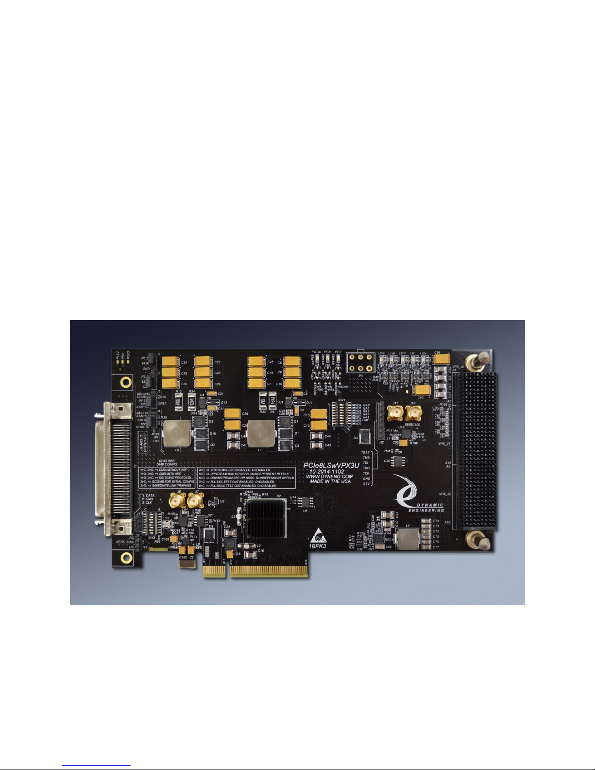
User Manual
PCIe8LSwVPX3U
PCIe 8 Lane VPX 3U Compatible Carrier
©2014-2017 by Dynamic Engineering.
Corresponding Hardware: Revision B
Fab number 10-2014-1102
Revision B3 10/19/17
Page 2

2
PCIe8LSwVPX3U
PCIe and VPX Compatible Carrier
Dynamic Engineering
150 Dubois St. Suite C
Santa Cruz, CA 95060
831457-8891
831457-4793 FAX
This document contains information of
proprietary interest to Dynamic Engineering. It
has been supplied in confidence and the
recipient, by accepting this material, agrees that
the subject matter will not be copied or
reproduced, in whole or in part, nor its contents
revealed in any manner or to any person except
to meet the purpose for which it was delivered.
Dynamic Engineering has made every effort to
ensure that this manual is accurate and
complete. Still, the company reserves the right to
make improvements or changes in the product
described in this document at any time and
without notice. Furthermore, Dynamic
Engineering assumes no liability arising out of
the application or use of the device described
herein.
The electronic equipment described herein
generates, uses, and can radiate radio
frequency energy. Operation of this equipment
in a residential area is likely to cause radio
interference, in which case the user, at his own
expense, will be required to take whatever
measures may be required to correct the
interference.
Dynamic Engineering’s products are not
authorized for use as critical components in life
support devices or systems without the express
written approval of the president of Dynamic
Engineering.
Connection of incompatible hardware is likely to
cause serious damage.
Other trademarks and registered trademarks are owned by their
respective manufactures.
Embedded Solutions Page
Page 3
3
PRODUCT DESCRIPTION 5
Clocking 7
Headers and TestPoints 8
DipSwitch Settings 9
Switch Status LED’s 11
VPX MODULE BACKPLANE IO INTERFACE PIN ASSIGNMENT 12
SCSI P2 – VPX J2 USER VPX P2 12
VPX Module J1 PCIe lane assignments 13
VPX Module J0 Power assignments 14
APPLICATIONS GUIDE 15
Interfacing 15
Construction and Reliability 16
Thermal Considerations 16
VITA Multipoint SSC Clocking implemenation 17
Loopback Testing 18
WARRANTY AND REPAIR 19
Service Policy 19
Out of Warranty Repairs 19
For Service Contact: 19
SPECIFICATIONS 20
Embedded Solutions Page
Page 4

4
ORDER INFORMATION 21
FIGURE 1 PCIE8LSWVPX3U CLOCKING 7
FIGURE 2 PCIE8LSWVPX3U P2/J2/USER P2 IO 12
FIGURE 3 PCIE8LSWVPX3U PCIE/J1 13
FIGURE 4 PCIE8LSWVPX3U POWER/J0 14
FIGURE 5 VITA SYSTEM CLOCKING – MAXIMUM CONFIGURATION 17
FIGURE 6 PCIE8LSWVPX3U LOOPBACK TEST CONFIGURATION 18
Embedded Solutions Page
Page 5

5
Product Description
PCIe8LSwVPX3U is part of the Dynamic Engineering PCI and VPX Compatible family
of modular I/O components. PCIe8LSwVPX3U adapts a 3U VPX device to one PCIe
position.
PCIe8LSwVPX3U features a 16 lane switch buffering the connection between the Gold
fingers on the PCIe side and the VPX connector. The switch provides isolation to allow
the VPX side to operate at a different Gen level than the upstream port, and to provide
clock domain separation. In many cases it is desirable to have the upstream port run
Spread Spectrum enabled, and the VPX side operate with a fixed frequency clock. The
switch is Gen3 compliant and can operate with Gen 1, 2 or 3 on either port.
New with Revision B, PCIe8LSwVPX3U has support for both SSC and NSSC clocking
on the VPX port. REF_CLK is supported with a 25 MHz SSC. The switch can be
programmed via dipswitch to use SSC or NSSC on the downstream port. The installed
VPX card will need to match the settings for proper operation.
Extended testing has been performed in both modes using the VPX8LXMC3U adapter
and an installed XMC-Parallel-TTL. DMA operations were run overnight multiple times
in both modes without failure or TLP corrections required at the switch.
VPX devices have 3 connectors for Power, Bus IF, and IO respectively.
The power connector supplies 5V, 3.3V and 12V. PCIe has +12V available. Local
power supplies generate the 3.3V and 5V for the VPX module. Approximately 10A are
available on each rail. Voltage monitor circuits check under and overvoltage conditions
of each rail including the ones for the switch, and illuminate an LED when the voltage is
within tolerance.
The Bus IF connector provides up to 8 lanes from the downstream port on the switch.
Differential routing with length and impedance control are maintained for all relevant
PCIe signals on both sides of the switch.
The IO is routed from the VPX rear IO connector through to a SCSI connector mounted
at the bezel of PCIe8LSwVPX3U. Differential routing with impedance control and
matched length traces are employed.
Embedded Solutions Page
Page 6

6
Special features:
• 8 lane PCIe interface
• DIP switch to configure and select:
- Switch/board PCIe NSSC or VITA Spec SSC
- PLX PEX8718 internal register access modes.
• Voltage monitors, each with LED’s on plus 12V, 5V, 3.3V, .9V and 1.8V
• 10A regulator for VPX 3.3V and 5V supplies. 12V from PCIe interface or optional –AP
connector.
• Front panel connector access through PCIe bracket for Rear IO
• User IO P2/J2 available through SCSI connector. Routed as differential pairs,
matched length, controlled impedance.
• JTAG programming support – optional header routed to VPX JTAG pins
• DIP switch to select global addressing on VPX
• PCIe Switch Status LED’s for FATAL, Port Good0, and Port Good1
• Optional EEPROM to configure PCIe Switch registers before boot.
• With Rev B cards, coax [SMA] are supplied on the SSC and NSSC ports to support
T&I
PCIe8LSwVPX3U is ready to use with the default settings. Just install the VPX onto the
PCIe8LSwVPX3U and then into the system. The board is designed to allow the use of
the PCIe8LSwVPX3U + VPX with other 1/2 length cards in the system.
For example we have a test set-up for a VPX card [VPX-RCB] with differential IO. We
use PMC-BiSerial-III to act as a system simulator. PCIeBPMC + PMC BiSerial III in the
front slot to create, and read back the IO. PCIe8LSwVPX3U + VPX in the second slot
for test. The BiSerial also has a SCSI connector allowing easy connection between the
bezels for a complete test path.
Embedded Solutions Page
Page 7
7
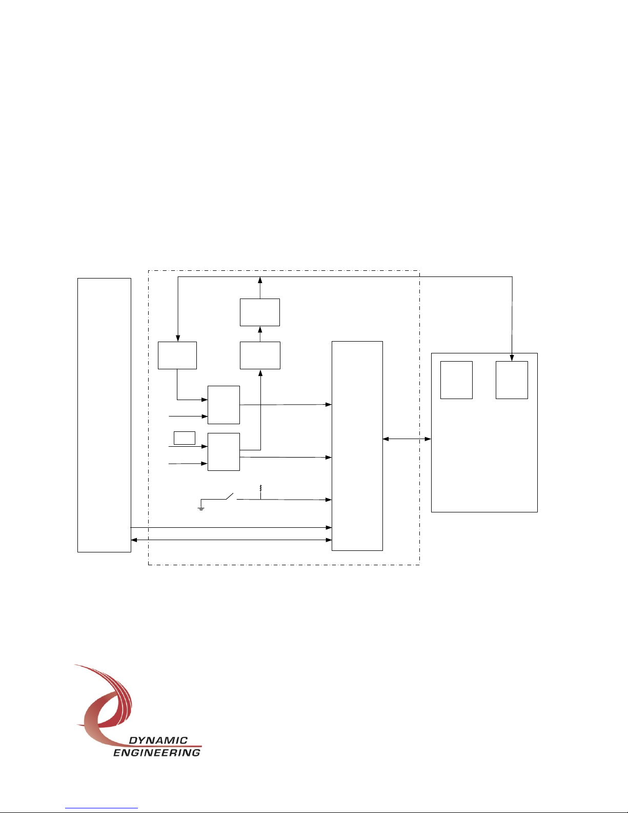
Clocking
PCIe8LSwVPX3U Clocking
EIA-899 M -LVDS
25MHz REFCLK +/-
with Mo dulation
+/- 100ppm max
50% duty cycle +/- 5%
PCI Express
Host
PCI
Express
Switch
VPX Add-In Card or
Carrier such as
Dynamic Engineering’s
VPX8LXMC3U
x8 PCIe link
REFCLKp/n
VPX/PCIe
Compliant
Downstream
Ports Clock
with Spread
Upstream
Port Clock with
Spread or
No Spread
X8 PCIe link
SSC Off
25MHz
Crystal
PCIe compliant
100MHz Clock
No Spread
Straps
Clock
Generator
SSC Off
Straps
25MHz in
100MHz out
with SSC
Generator
1.8V
M-LVDS
Transmitter
25MHz
100MHz
25MHz in
25MHz SSC out
Clock Generator
M-LVDS
Receiver
Note: VPX Spec allows up to 32
circuits to be connected to the
common transmission media
Backplane differential REF_CLK+/- lines are differentially
terminated at each end with a resistor of 61.9 Ohms +/- 1%
PCIe
Compliant
Downstream
Ports Clock
No Spread
Downstream
Port
Clock Select
PCIe compliant
100MHz Clock
with Spread
VITA
25MHz in
100MHz out
with SSC
Generator
PCIe
Compliant
100MHz
NSSC
Generator
AND
OR
PCIe8LSwVPX3U VPX (PCIe downstream) port supports both PCI Express
Independent Non-Spread Spectrum Clocking (NSSC) and VITA Spread Spectrum
Clocking (SSC). The upstream/host port supports a PCIe REFCLK that is either a SSC
or a NSSC, or can be configured to use an on board NSSC if desired. Figure 1 shows
the clocking architecture of the PCIe8LSwVPX3U. The clocking mode is selected using
DIP Switches described in the DIP switch settings section.
FIGURE 1 PCIE8LSWVPX3U CLOCKING
Embedded Solutions Page
Page 8

8
Headers and TestPoints
H2 is an optional JTAG header used to connect to VPX J0. The pin definitions are in
the silk. 1: 3.3V, 2: GND, 6: TMS, 4: TDO, 5: TDI, 3: TCK. Pin numbering matches
flying lead breakout on Xilinx programmer. Other vendor programmers can also be
used.
J1 is an optional use header to support the serial bus connection to the Switch. 1 =
SMDAT [pull-up 4.7K to 3.3V] 2 = gnd, 3 = SMCLK [pull-up 4.7K to 3.3V].
J2 & J3 control the voltage on 33, 67 and 34, 68 of P2 respectively. 1-2 selects 3.3V
and 2-3 selects ground on those pins. The shunt and traces are rated for 1A. Not fuse
protected.
J4 & J5 control the timing of the 3.3V and 5V power supplies. 1-2 selects delayed, 2-3
selects immediate, open selects off. J4 controls 3.3V and J5 controls 5V.
J7(p) & J8(n) are SMA connectors tied to the NSSC 100 MHz. These connectors can
be used as a reference to the clock used by the Switch in NSSC mode.
J9(p) & J10(n) are SMA connectors tied to the SSC 100 MHz. These connectors can
be used as a reference to the clock used by the Switch in SSC mode.
(J6 and J11 are unused reference designators)
J12 control the reference on the PCIe bezel. 1-2 selects AC coupled 2-3 selects DC
coupled and open is uncoupled to ground.
P3 is an optional power connector to allow for added 12V power to be used by the
PCIe8LSwVPX3U. The PCIe gold fingers allow for about 60W of power to be
consumed by the board across all VPX voltages including power supply losses. In
many cases the power budget is more than sufficient. If your VPX requires more power
please request the optional power connector [6 wire standard PC 2x3] to increase the
12V available. Both 12V entry points are diode coupled to prevent the current backfeeding when an external or other supply is added.
P3: 1, 2, 3= 12V, 4, 5, 6 = gnd.
Embedded Solutions Page
Page 9

9
DipSwitch Settings
SW1 (Switch 1): Global Address Settings
Position 1-5 corresponds to GA0-4. ‘0’ when closed (C). ‘1’ when open (O).
Position 6 corresponds to GAP. ‘0’ when closed (C). ‘1’ when open (O).
Position 7-8 are spare
SW2 (Switch 2): PCIe Switch and Clock Operation Settings
C = Closed, O = Open
Below are the standard settings that are used to configure the PCIeLSwVPX3U VPX
port for either NSSC or SSC operation. Details of each switch setting is also provided.
For NSSC (Non Spread Spectrum Independent Clocking) SW2 is set as follows:
8 O -- Disable 100MHz NSSC on J7 and J8
7 O -- Disable 100MHz SSC on J10 and J11
6 C -- Selects 100MHz NSSC to be used by PCIe Switch’s downstream port
5 O -- Selects PCIe REFCLK to be used by PCIe Switch’s upstream port
4 C -- Disable 25MHz SSC clock output
3 O -- I2C/SMBus not used for initial device configuration
2 C -- Selects I2C protocol
1 O -- Selects I2C protocol
For SSC (VITA spec Spread Spectrum Clocking) SW2 is set as follows:
8 O -- Disable 100MHz NSSC on J7 and J8
7 O -- Disable 100MHz SSC on J10 and J11
6 O -- Selects 100MHz SSC to be used by PCIe Switch’s downstream port
5 O -- Selects PCIe REFCLK to be used by PCIe Switch’s upstream port
4 O -- Enable 25MHz SSC clock output
3 O -- I2C/SMBus not used for initial device configuration
2 C -- Selects I2C protocol
1 O -- Selects I2C protocol
Embedded Solutions Page
Page 10

10
Switch 2,1 – Selects protocol used for initial configuration and/or register access
OO SMBus with ARP (Address Resolution Protocol)
OC SMBus without ARP
CX I2C (default setting)
Switch 3 – Enables/Disables use of I2C/SMBus for initial PCIe Switch configuration.
O I2C/SMBUS NOT used for initial configuration (default setting)
C I2C/SMBUS is used for initial configuration.
Note: EEPROM can be used with either setting.
Switch 4 – 25MHZ VPX REFCLK Enable
O 25MHZ VPX REFCLK Enabled/ON
C 25MHZ VPX REFCLK Disabled/OFF
Switch 5 – PCIe Switch Upstream port clock select
O Upstream port uses PCIe REFCLK from PCIe connector (default setting)
C Upstream port uses 100MHz NSSC generated on board
Switch 6 – PCIe Switch Downstream port clock select
O Downstream port uses 100MHz SSC generated from 25MHZ VPX REFCLK
C Downstream port uses 100MHz NSSC generated on board
Switch 7 – Enables/Disables copy of 100MHz SSC to be output on SMA connectors
O SSC is NOT output on SMA Connectors J10 and J11
C Copy of 100MHz SSC is output on SMA Connectors J10 and J11
Switch 8 – Enables/Disables copy of 100MHz NSSC to be output on SMA connectors
O NSSC is NOT output on SMA Connectors J7 and J8
C Copy of 100MHz NSSC is output on SMA Connectors J7 and J8
Embedded Solutions Page
Page 11

11
Switch Status LED’s
There are three PCIe Switch status LED’s.
° The left hand LED is for FATAL which is illuminated for an unrecoverable error.
° The Middle LED is for the upstream Port status.
° The right hand LED is for the downstream port status.
The upstream port is connected to the PC and the downstream to your installed HW.
Steady on means Gen3 communications, Flashing 2x per second means Gen2 and
Flashing 1 time per second means Gen1. Off means link is not operating. Please
note: if PCIe8LSwVPX3U is installed in the PC with no User HW present the
downstream port LED will be off.
Embedded Solutions Page
Page 12

12
VPX Module Backplane IO Interface Pin Assignment
The figure below gives the pin assignments for the VPX Module IO Interface – from
P2/J2 to the PCIe8LSwVPX3U connector. Also see the User Manual for your VPX
board for more information.
SCSI P2 – VPX J2 USER VPX P2
SCSI II [P2] VPX[J2] User VPX [P2]
1 35 G16 H16 E16 F16
2 36 C16 D16 B16 C16
3 37 E15 F15 D15 E15
4 38 A15 B15 A15 B15
5 39 G14 H14 E14 F14
6 40 C14 D14 B14 C14
7 41 E13 F13 D13 E13
8 42 A13 B13 A13 B13
9 43 G12 H12 E12 F12
10 44 C12 D12 B12 C12
11 45 E11 F11 D11 E11
12 46 A11 B11 A11 B11
13 47 G10 H10 E10 F10
14 48 C10 D10 B10 C10
15 49 E9 F9 D9 E9
16 50 A9 B9 A9 B9
17 51 G8 H8 E8 F8
18 52 C8 D8 B8 C8
19 53 E7 F7 D7 E7
20 54 A7 B7 A7 B7
21 55 G6 H6 E6 F6
22 56 C6 D6 B6 C6
23 57 E5 F5 D5 E5
24 58 A5 B5 A5 B5
25 59 G4 H4 E4 F4
26 60 C4 D4 B4 C4
27 61 E3 F3 D3 E3
28 62 A3 B3 A3 B3
29 63 G2 H2 E2 F2
30 64 C2 D2 B2 C2
31 65 E1 F1 D1 E1
32 66 A1 B1 A1 B1
33 67 Open, +3 or GND via J1 silk screen defined
34 68 Open, +3 or GND via J2
FIGURE 2 PCIE8LSWVPX3U P2/J2/USER P2 IO
Read table:
P2-1 = J2-G16, P2-35 = J2-H16
GND1-72 are connected to GND. C1, D1 etc. SE7-0 are open I1, I3, I5 etc.
Embedded Solutions Page
Page 13

13
VPX Module J1 PCIe lane assignments
Signal J1
LN0-RX+ LN0-RX- A1 B1
LN0-TX+ LN0-TX- E1 F1
LN1-RX+ LN1-RX- C2 D2
LN1-TX+ LN1-TX- G2 H2
LN2-RX+ LN2-RX- A3 B3
LN2-TX+ LN2-TX- E3 F3
LN3-RX+ LN3-RX- C4 D4
LN3-TX+ LN3-TX- G4 H4
LN4-RX+ LN4-RX- A5 B5
LN4-TX+ LN4-TX- E5 F5
LN5-RX+ LN5-RX- C6 D6
LN5-TX+ LN5-TX- G6 H6
LN6-RX+ LN6-RX- A7 B7
LN6-TX+ LN6-TX- E7 F7
LN7-RX+ LN7-RX- C8 D8
LN7-TX+ LN7-TX- G8 H8
FIGURE 3 PCIE8LSWVPX3U PCIE/J1
GND1-72 are connected to GND. C1, D1 etc. VPX0_DEF&P1-SE7-4 are open I1, I3,
I5 etc.
Please note: (1) VPX definitions are relative to VPX. PCIe connector definitions are
relative to the PCIe bus. PCIe8LSwVPX3U reverses the lanes [TX/RX] between the
switch connections and the VPX J1 connector to compensate.
(2) VPX standard does not support the PCIe reference clock, but does support
independent clocking and SSC using a lower frequency REFCLK. It is expected the
VPX will provide a local reference clock. The PCIe Switch isolates Upstream from VPX
side.
Embedded Solutions Page
Page 14

14
VPX Module J0 Power assignments
Signal J0
GND A4, A5, A6, A8, B8, C7, D4, D5, D6, D7, E8, F4, F5, F6, F8, G7, H7, I4, I5, I6, I8
12V F1, F2, G1, G2, H1, H2, I1, I2
3.3V A1, A2, B1, B2, C1, C2, D1, D2
5V A3, B3, C3, D3, F3, G3, H3, I3
3.3V AUX E5
M12 AUX OPEN
P12AUX OPEN
PERST# C4
FIGURE 4 PCIE8LSWVPX3U POWER/J0
Note: 3.3V Aux is routed to PCIe 3.3V Aux and will be powered from PC power supply
as defined by your PC. PERST# is the PCIe reset signal and is also routed to this
connector. Global addressing and JTAG pin definitions shown in the header/switch
section of this manual.
Embedded Solutions Page
Page 15

15
Applications Guide
Interfacing
Some general interfacing guidelines are presented below. Do not hesitate to contact the
factory if you need more assistance.
Installation
The VPX is mounted to the PCIe8LSwVPX3U prior to installation within the chassis.
PCIe8LSwVPX3U is fitted with VPX compliant mounting / alignment pins. J0 is toward
the top of the card. The alignment pins are offset to provide keying to prevent improper
card installation. Rocking the VPX slightly during installation can help with the process
of installation. The blades have proven to be quite robust, however; the connectors are
expensive so be careful.
Since the VPX is mounted at right angles to the adapter the weight of the VPX is
cantilevered out from the PCIe card. If mounted in a chassis and the bezel is screwed
in place you may be ok. If not you will need to support the VPX. We have found
stacking Lego’s to be a very handy approach as the height can be altered to match the
set-up and the wide base is stable.
The IC’s will be on the outside – toward the right when viewing the component side of
the PCIe8LSwVPX3U. This will allow for full access to your devices when probing. We
use with an open chassis – no frame – to allow for better access to everything.
The JTAG header can be installed on the rear of PCIe8LSwVPX3U to keep the JTAG
programmer out of the way when working on the installed VPX. This will also allow the
VPX to be swapped out without disconnecting the JTAG programmer.
Start-up
Make sure that the "system" can see your hardware before trying to access it. Many
BIOS will display the PCI/PCIe devices found at boot up on a "splash screen” with the
VendorID and CardID for the VPX installed and an interrupt level. If the information is
not available from the BIOS then a third party PCI device cataloging tool will be helpful.
Watch the system grounds. All electrically connected equipment should have a failsafe common ground that is large enough to handle all current loads without affecting
noise immunity. Power supplies and power consuming loads should all have their own
ground wires back to a common point.
Embedded Solutions Page
Page 16

16
Power all system power supplies from one switch. Connecting external voltages to
the PCIe8LSwVPX3U when it is not powered can damage it, as well as the rest of the
host system. This problem may be avoided by turning all power supplies on and off at
the same time. This applies more to the VPX installed onto the PCIe8LSwVPX3U than
the PCIe8LSwVPX3U itself, and it is smart system design when it can be achieved.
Construction and Reliability
The PCIe8LSwVPX3U is constructed out of 0.062 inch thick high temp RoHS compliant
FR4 material. The components on the PCIe8LSwVPX3U are tied into the internal
power planes to spread the dissipated heat out over a larger area. This is an effective
cooling technique in the situation where a large portion of the board has little or no
power dissipation.
The VPX Module connectors are keyed and shrouded with Gold plated pins on both
plugs and receptacles. The current rating varies with the blade type. At the moment
Tyco is the only vendor providing VPX connectors.
Thermal Considerations
If the VPX installed has a large heat dissipation; forced air cooling is recommended.
Embedded Solutions Page
Page 17

17
VITA Multipoint SSC Clocking implementation
PCIe8LSwVPX3U VITA System Clocking – Maximum Configuration
EIA-899 M -LVDS
25MHz REFCL K +/-
with Mo dulation
+/- 100ppm max
50% duty cycle +/- 5%
PCI Express
Host
PCI
Express
Switch
VPX Add-In Card29
VPX Add-In Card0
VPX Add-In Card1
VPX Add-In Card2
.
.
PCIe link
REFCLKp/n
VPX/PCIe
Compliant
Downstream
Ports Clock
with Spread
Upstream
Port Clock with
Spread or
No Spread
PCIe link
PCIe link
PCIe link
PCIe link
SSC Off
25MHz
Crystal
PCIe compliant
100MHz Clock
No Spread
Straps
Clock
Generator
SSC Off
Straps
25MHz in
100MHz out
with SSC
Generator
1.8V
M-LVDS
Transmitter
25MHz
100MHz
25MHz in
25MHz SSC out
Clock Generator
M-LVDS
Receiver
Note: VPX Spec allows up to 32 circuits to be
connected to the common transmission media
Backplane differential REF_CLK+/- lines are differentially terminated at each end with a resistor of 61.9 Ohms +/- 1%
PCIe
Compliant
Downstream
Ports Clock
No Spread
Downstream
Ports
Clock Select
PCIe compliant
100MHz Clock
with Spread
The VITA Specification defines, and the PCIe8LSwVPX3U circuits support the VITA
maximum of 32 circuits connected together on a common transmission media.
The PCIe8LSwVPX3U implements this feature per VITA specification by generating,
supplying, and using a common 25MHz VITA SSC that is transmitted and received
using M-LVDS differential transceivers. The PCIe8LSwVPX3U can be optionally
configured to provide and use its VITA 25MHz SSC to supply the PCIe Switches’
downstream port with a 100MHz SSC clock generated from the received 25MHz VITA
SSC. Dynamic Engineering has validated the PCIe8LSwVPX3U VITA 25MHz SSC
clocking design using Dynamic Engineering VPX8LXMC3U carrier (also supports VITA
SSC clocking) and the XMC-PARALLEL-TTL board. Figure 5 shows the maximum
configuration of 32 circuits connected together.
FIGURE 5 VITA SYSTEM CLOCKING – MAXIMUM CONFIGURATION
Embedded Solutions Page
Page 18

18
VPX8LXMC3U
LOOPBACK
FIXTURE
PCIe8LSwVPX3UXMC-Parallel-TTL
PCI Express
Host
SCSI
P2
VPX
J2
32--->16
28--->12
24--->8
20--->4
31--->15
27--->11
23--->7
19--->3
66--->50
62--->46
58--->42
54--->38
65--->49
61--->45
57--->41
53--->37
30--->14
26--->10
22--->6
18--->2
29--->13
25--->9
21--->5
17--->1
64--->48
60--->44
56--->40
52--->36
63--->47
59--->43
55--->39
51--->35
Loopback Testing
For both the validation of, and the ATP for PCIE8LSwVPX3U, Dynamic Engineering
uses VPX8LXMC3U, XMC-PARALLEL-TTL, and a loopback fixture. Figure 6 shows the
validation and ATP test configuration.
FIGURE 6 PCIE8LSWVPX3U LOOPBACK TEST CONFIGURATION
SCSI P2 Loopback connections are as follows:
Embedded Solutions Page
Page 19

19
Warranty and Repair
Please refer to the warranty page on our website for the current warranty offered and
options.
http://www.dyneng.com/warranty.html
Service Policy
Before returning a product for repair, verify as well as possible that the suspected unit is
at fault. Then call the Customer Service Department for a RETURN MATERIAL
AUTHORIZATION (RMA) number. Carefully package the unit, in the original shipping
carton if this is available, and ship prepaid and insured with the RMA number clearly
written on the outside of the package. Include a return address and the telephone
number of a technical contact. For out-of-warranty repairs, a purchase order for repair
charges must accompany the return. Dynamic Engineering will not be responsible for
damages due to improper packaging of returned items. For service on Dynamic
Engineering Products not purchased directly from Dynamic Engineering contact your
reseller. Products returned to Dynamic Engineering for repair by other than the original
customer will be treated as out-of-warranty.
Out of Warranty Repairs
Out of warranty repairs will be billed on a material and labor basis. Customer approval
will be obtained before repairing any item if the repair charges will exceed one half of
the quantity one list price for that unit. Return transportation and insurance will be billed
as part of the repair and is in addition to the minimum charge.
For Service Contact:
Customer Service Department
Dynamic Engineering
150 DuBois St. Suite C
Santa Cruz, CA 95060
831-457-8891 831-457-4793 fax Internet Address support@dyneng.com
Embedded Solutions Page
Page 20

20
Specifications
Logic Interfaces: PCIe up to 8 lanes per VPX
Access types: Switch isolated PCIe interface, all modes supported.
CLK rates supported: Gen1, Gen2, Gen 3
Software Interface: Transparent design with no software required for adapter. Installed
VPX will determine control of that device.
Initialization: switch selections for Global Addressing if needed.
Interface: VPX rear IO [P2] via PCIe bracket mounted SCSI II connector
Dimensions: 1/2 length + PCIe board
Construction: High Temp FR4 Multi-Layer Printed Circuit, Through Hole and
Surface Mount Components.
Embedded Solutions Page
Page 21

21
Order Information
standard temperature range 070øC
PCIe8LSwVPX3U 1/2 length + PCIe card with VPX position
-ROHS [ROHS compliant parts and process]
-JTAG add JTAG header to rear of card
-AP add auxiliary power connector
http://www.dyneng.com/PCIe8LSwVPX3U.html
HDEterm68 http://www.dyneng.com/HDEterm68.html
68 pin SCSI II to 68 screw terminal converter with DIN
rail mounting.
HDEcabl68 http://www.dyneng.com/HDEcabl68.html
SCSI cables with latch blocks or thumbscrews and
various lengths are available. Custom lengths can be
ordered.
All information provided is Copyright Dynamic Engineering
Embedded Solutions Page
 Loading...