

Page 1

DYNAMIC ENGINEERING
150 DuBois, Suite C Santa Cruz, CA 95060
(831) 457-8891 Fax (831) 457-4793
www.dyneng.com
sales@dyneng.com
Est. 1988
User Manual
PCIeIP Carrier Series
PCI Express x1 to
IP (Industry Pack) Bridge
Models in Group :
PCIe3IP [Released]
PCIe5IP [Released]
VPX2IP [Released]
VPX4IP [Coming soon]
Revision A1.3
December 2016
©2013-2016 by Dynamic Engineering.
Other trademarks and registered trademarks are owned by their respective manufacturers.
Embedded Solutions Page 1 of 71
Page 2
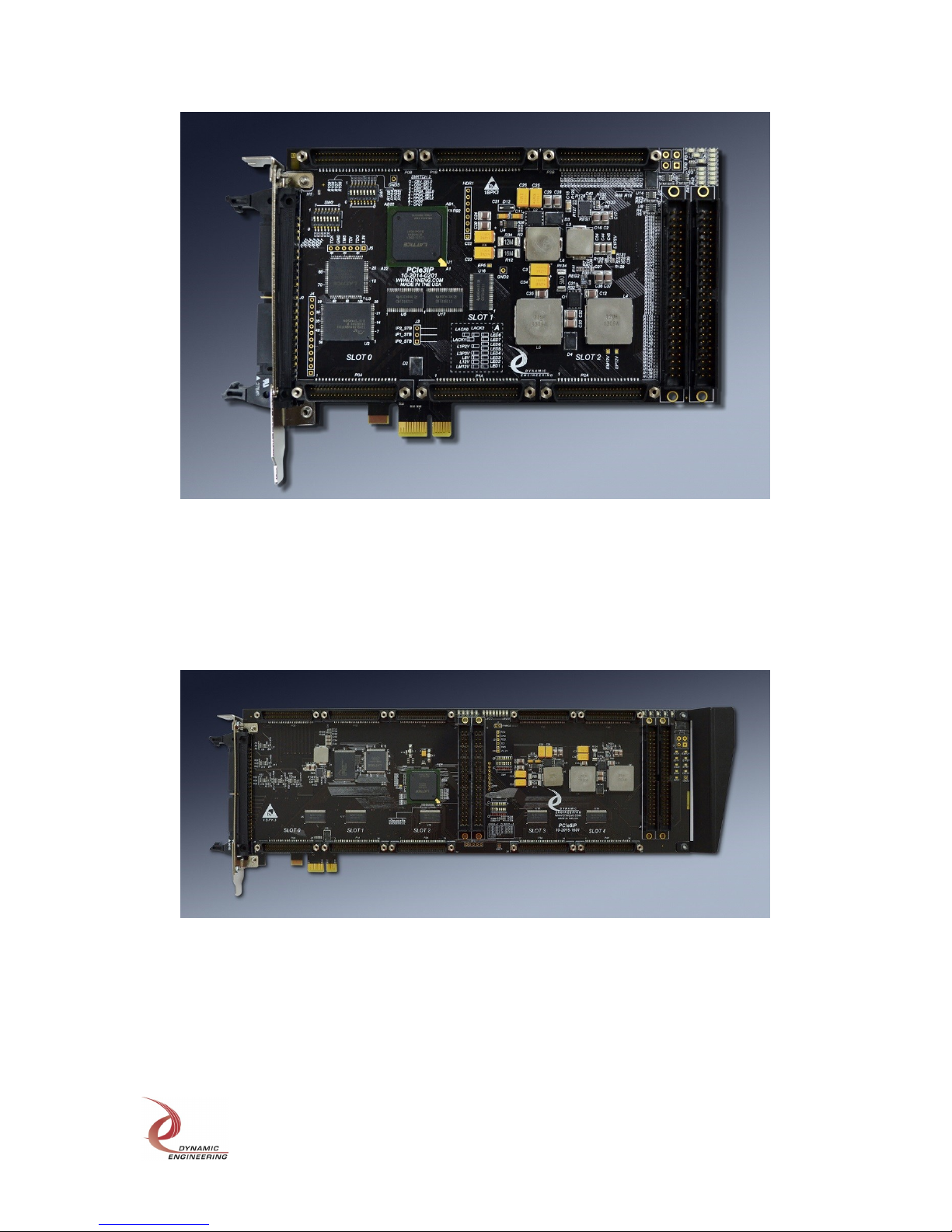
PCIe3IP: PCI Express carrier with 3 IP positions.
Fab Number: 10-2014-0202/3 FLASH Rev 0x10
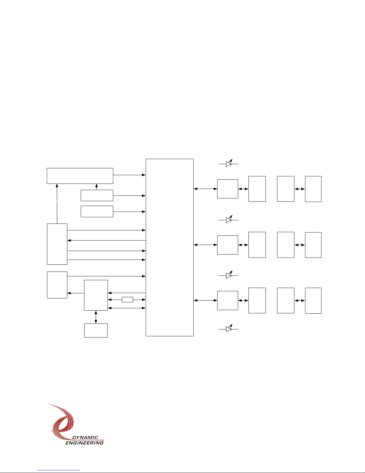
PCIe5IP: PCI Express carrier with 5 IP positions.
Fab Number: 10-2015-1601 FLASH Rev 0x10
E m b e d d e d S o l u t i o n s P a g e 2 o f 71
Page 3

VPX2IP: PCI Express carrier with 2 IP positions.
Fab Number: 10-2016-1901 FLASH Rev 0x10
E m b e d d e d S o l u t i o n s P a g e 3 o f 71
Page 4

PCIeIP Carrier Series
PCI Express x1 to
IP (Industry Pack) Bridge
Dynamic Engineering
150 DuBois St. Suite C, Santa Cruz CA 95060
831-457-8891 831-457-4793 FAX
This document contains information of proprietary interest to Dynamic Engineering. It
has been supplied in confidence and the recipient, by accepting this material, agrees
that the subject matter will not be copied or reproduced, in whole or in part, nor its
contents revealed in any manner or to any person except to meet the purpose for which
it was delivered.
Dynamic Engineering has made every effort to ensure that this manual is accurate and
complete. Still, the company reserves the right to make improvements or changes in the
product described in this document at any time and without notice. Furthermore,
Dynamic Engineering assumes no liability arising out of the application or use of the
device described herein.
The electronic equipment described herein generates, uses, and can radiate radio
frequency energy. Operation of this equipment in a residential area is likely to cause
radio interference, in which case the user, at his own expense, will be required to take
whatever measures may be required to correct the interference.
Dynamic Engineering’s products are not authorized for use as critical components in life
support devices or systems without the express written approval of the president of
Dynamic Engineering.
This product has been designed to operate with IndustryPack Modules and compatible
user-provided equipment. Connection of incompatible hardware is likely to cause
serious damage.
E m b e d d e d S o l u t i o n s P a g e 4 o f 71
Page 5

PRODUCT DESCRIPTION 9
Table of Contents
THEORY OF OPERATION 16
PROGRAMMING 18
VPX2IP ADDRESS MAP 18
PCIE3IP ADDRESS MAP 19
PCIE5IP ADDRESS MAP 20
PCIEIP RESETS, CLOCKS, & BUS ERROR 22
IP CHANNEL TRANSFER ACTIVITY MONITOR AND LOGIC 26
PCIEIP INTERRUPTS 28
PCIEIP REGISTERS 37
LED DECODE TABLE 49
PCIEIP BOARD FEATURES 52
PCIeIP Carrier IP Logic Connector Pin Assignment 52
PCIeIP IP Carrier IO Connector to 50 Pin Header Assignment 53
VPX2IP IP Carrier Condo Header Connector Assignment – Option 1 53
VPX2IP IP Carrier Rear IO Connector Assignment – Option 2 54
PCIE3IP BOARD FEATURES 55
PCIe3IP DIP Switches 55
Embedded Solutions Page 5 of 71
Page 6

PCIe3IP LED’s 56
PCIe3IP IP1/IP2 connectivity option 57
PCIe3IP Board Revision 58
PCIE5IP BOARD FEATURES 59
PCIe5IP DIP Switches 59
PCIe5IP LED’s 60
PCIe5IP Board Revision 61
VPX2IP BOARD FEATURES 62
VPX2IP DIP Switches 62
VPX2IP LED’s 63
VPX2IP IP0/IP1 connectivity options 64
VPX2IP Board Revision 65
MECHANICAL 66
APPLICATIONS GUIDE 66
ELECTRICAL 66
AC/DC TIMING 66
INTERFACING 66
CONSTRUCTION AND RELIABILITY 67
THERMAL CONSIDERATIONS 67
WARRANTY AND REPAIR 68
Service Policy 68
Out of Warranty Repairs 68
Embedded Solutions Page 6 of 71
Page 7

For Service Contact: 68
SPECIFICATIONS 69
ORDER INFORMATION 71
Embedded Solutions Page 7 of 71
Page 8

List of Figures
Figure 1 PCIe3IP Block Diagram 14
Figure 2 PCIe3IP FPGA Block diagram 15
Figure 3 VPX2IP Base Address Map 18
Figure 4 PCIe3IP Base Address Map 19
Figure 5 PCIe5IP Base Address Map 20
Figure 6 PCIeIP Register Address Map 38
Figure 7 PCIeIP IP Logic Interface 52
Figure 8 PCIeIP IP I/O to 50 pin Header Connections 53
Figure 9 VPX2IP IP Carrier Rear IO Connector Assignment 54
Figure 10 PCIe3IP IP[2:0] I/O to 50 pin J[2:0] Header Diagram 57
Figure 11 VPX2IP IP[1:0] I/O to Condo Header or Rear IO (VPX) connector Diagram 64
Embedded Solutions Page 8 of 71
Page 9

Product Description
The PCIeIP Carrier Series is part of Dynamic Engineering’s IP Compatible family of
modular I/O components. The PCIeIP Carrier Series uses a single PCI Express (PCIe)
slot or lane (VPX). Products in the PCIeIP Carrier Series covered by this manual
include:
1) PCIe3IP - A half-length card providing three IndustryPack Compatible sites.
2) PCIe5IP - A full-length card providing five IndustryPack Compatible sites.
3) VPX2IP - A 3U 4HP with bezel or rear IO card providing two IndustryPack
Compatible sites.
IndustryPack ID, IO, INT, and MEM access types are supported for read and write
cycles. The full 8 Mbytes of address space is allocated to each of the MEM spaces.
Low impedance Quick Switch devices provide a signaling bridge between the 3.3V
FPGA signaling and 5V IP signaling environments. A user switch setting can select the
IP bus to operate at 3.3V. Users can take advantage of the 3.3V signaling by removing
their level shifting devices. Module positions are independent for reference voltage
selection.
The PCI Express link is a by one (x1) link that is fully compliant to PCI Express 1.1
revision of the PCI-SIG specification and as such can operate in any compliant PCIe
Gen1, Gen2, Gen3, or Gen4 slot. Each IP position supports 8 & 16 bit IP devices and is
fully compliant to the Vita 4-1995 specification.
Each IndustryPack module position has a completely separate IP control bus
connection to the FPGA. Within the FPGA each of the IP control buses are separately
controlled. Packets received from the PCIe link are routed through steering logic to the
proper control bus interface. Within each control interface FIFOs are used to store
multiple packets. With this architecture multiple IndustryPack data transfers can be
queued for execution as the IP is ready. One advantage of this architecture is that a
slower IP does not hold up a faster IP from being serviced. Also a loop to load a FIFO
or fill RAM etc. can potentially be completely adsorbed by PCIeIP allowing the CPU to
move onto other tasks much faster.
Since some situations require deterministic execution and coordination between
installed IndustryPack modules, design features are provided to control the execution of
commands in a specific sequence between multiple IP modules. Since all instructions
are executed in order, this mode is not needed for single IP deterministic operation.
Embedded Solutions Page 9 of 71
Page 10

Per the PCIe specification every access is at least a one long word. Byte, word, and
3byte accesses are supported utilizing PCIe byte enables. Any combination of byte
enables and starting address as defined by the PCIe specification is supported. The
PCIeIP supports PCIe transfer sizes of 1 and 2 long words (2Lwords = 1 quad word).
PCIe accesses are automatically converted into IP accesses and may range from a
single IP access up to 4 back-to-back IP accesses with the IP address incrementing
between cycles unless the address increment disable function is selected. For a read,
the IP read data is assembled, and a PCIe read completion packet is returned. The
Automatic generation of IP accesses greatly enhances the overall throughput when
transfers are > 2 bytes. Additionally, based on the PCIe byte enables the PCIeIP
determines when only a single 16 bit IP access needs to be performed for word or byte
transfers. In all cases the appropriate IP byte lane enables are applied as necessary.
Each IP clock is independently programmable for 8 or 32 MHz operation via a bit in its
control register. By default each IP CLK is 8MHz after power up and/or reset. The clock
frequency maybe changed at any time without consequence. Regardless of the
frequency of each clock, the IP clock outputs are designed to be “phase stepped” in
relation with one another to reduce simultaneous switching noise. For the PCIe3IP and
PCIe5IP the rising edge of IP1 clock is 8ns and IP2 clock is 16ns after the rising edge of
IP0’s clock. The PCIe5IP IP3/4’s clock is in phase with IP0/1’s clock. For the VPX2IP
the rising edge of IP1 clock is 8ns after the rising edge of IP0’s clock.
In normal operation IP access latency and performance is substantially better and the IP
logic runs 4 times faster when the IP CLK is 32MHz versus 8MHz.
PCIeIP has a programmable watchdog timer function, which completes the IP access if
the IP does not respond within the required amount of clock cycles. The watchdog timer
has a status bit and an optional Bus Error interrupt output.
PCIeIP supports interrupts from each IP slot with separate mask bits. Two interrupts
from each IP slot are supported. An interrupt force bit is available to aid in software
development in addition to the IP required 5V Power Good interrupt. All the interrupts
are maskable. The masked interrupt output signals are tied together and if asserted will
generate either MSI or INTA#.
PCIeIP has several programmable interrupt features to control when an interrupt is
generated. Programmable bits select behavior such as edge or level, or aggregation
timer values to pace the rate at which interrupts are generated (see Interrupt section for
details).
Embedded Solutions Page 10 of 71
Page 11

VPX2IP/PCIe3IP/PCIe5IP has a total of 15/16/18 LED’s to indicate various status. 2/3/5
LED’s are used and light to indicate ACK* activity on each of the 2/3/5 IP channels. 5
LED’s are used with 5 independent voltage monitoring circuits to accurately detect if any
of the board’s voltages are out of range. One LED for each power monitoring circuit,
when the LED is on the voltage is in range, if the LED is off the voltage is out of range.
Eight (8) user controllable LED's are supplied. Each LED is programmable with one of
sixteen possible sources to provide a variety of status. The 4bit LED select field in the
Switch and LED control register is used to determine each LED’s meaning. One of the
selections allows the user to directly control the LED’s. The default selection uses 4
LED’s to reflect PCIe link status, when all four of the lower four LED’s are on they
indicate a working link.
Two 8 bit "dip switches" are provided on the PCIeIP. One 8 bit dip switch is for user
configuration and is readable via the Switch and LED control register. The other 8 bit dip
switch is for board configuration and test purposes (see Board Features section for
details).
Power-on PCIe PERST# reset is used to reset the entire PCIeIP. Each IP Reset* is
asserted as long as PERST# is asserted. Once PERST# is de-asserted each IP’s clock
starts toggling, and each IP Reset* will remain asserted until a 256ms timer expires.
Once the timer expires IP Reset* de-asserts synchronously with that IP’s CLK. Two
separate control register reset bits are provided for each IP. One only asserts IP Reset*,
and one asserts IP Reset* and resets that PCIeIP’s IP channel/FIFO.
To meet the PCI Express specification requirement for PCIe core initialization within
100mS from PERST# de-assertion; PCIeIP implements a 16 bit wide 90ns Flash in
conjunction with a CPLD to configure the FPGA via its parallel configuration port. With
this architecture, PCIeIP beats this aggressive specification by a comfortable margin.
For the PCIe3IP/PCIe5IP the IO’s for each IP are brought out to their own 50 pin
headers. For the VPX2IP, stuffing options route the IO to either the Condo header or the
VPX rear connector. All IO signals for each PCIeIP board are routed carefully with
matched length and impedance control. Differential routing techniques are used to
support operation with LVDS, RS485 and other differential electrical standards as well
as single ended systems – analog, TTL IO etc. Please see the pin-out tables later in
this manual for the mapping of IP IO to header.
For the PCIe3IP/PCIe5IP the 50 pin header in the first position is mounted [right angle
header] to be accessible through the bezel. The second, third, (PCIe3IP) fourth and
fifth positions (PCIe5IP) have traditional vertical headers.
Embedded Solutions Page 11 of 71
Page 12

The bezel for the PCIe3IP is a special design with accommodation for the right angle
header and cable routing for the other two. All of the IO can come through the bezel
without wasting another IO position. The bezel incorporates an arm with hinge to allow
the side of the bezel to be rotated out of the way to aide in threading the rear IO through
the bezel. Install the IO into the rear headers, lift the bezel arm, place the cabling onto
the bezel, rotate the arm back into position, and mount into the system.
PCIeIP conforms to the VITA standard for IndustryPack Carriers. This guarantees
compatibility with multiple IndustryPack compatible modules.
Dynamic Engineering provides Windows, Linux and VxWorks drivers for the PCIeIP.
The drivers detect the carrier card and communicate with the OS to get the memory,
interrupts etc. assigned to the installed carrier. The driver interrogates the IP positions
on the carrier and when an IP is located determines if a corresponding driver is
installed. If not the IP-Generic driver is installed to allow any third party IP module to
be used with the carrier. When a recognized module is detected the driver for that
module is installed automatically.
Embedded Solutions Page 12 of 71
Page 13

Feature List Summary
• 2/3/5 IP compatible slots VPX2IP/PCIe3IP/PCIe5IP
• 8 or 32 MHz operation in each slot independently programmable
• IP CLK phase stepper – reduces simultaneous switching noise
• PCI Express Gen1, Gen2, Gen3, or Gen4 slot operable and compliant
• Non-blocking IP FIFO architecture - prevents IP versus IP packet congestion
• MSI and INTA# Interrupt support
• Programmable Interrupt pacing/aggregation with edge or level detection
• IP Channel Activity Monitors - ACK* Counters & Logic enable sequenced IP transfers
• byte, word, long word, and quad word transfer capable
• Incrementing or static address access of each IP slot
• Programmable IP Word and/or Byte Swapping
• Programmable Bus error abort response times
• 5 independent voltage monitoring circuits – to detect if a board voltage is out of range
• 1:1 50 pin headers with matched 5 mill trace & spacing widths between IO and header
• IP1/IP2 I/O SMT to 50 pin headers trace configuration/stuffing options - PCIe3IP only
• Configurable IO routing to Condo header or VPX Rear IO connector – VPX2IP only
• Individual IP resets with options for IP only or IP and local control
• Two 8 position "DIP Switches” – one for users, one for configuration and test
• Configurable IP Bus Termination – select 5.0V or 3.3V termination via CFG switches
• 8 User LED's, 5 Power good indicator LED's, an ACK* activity LED for each IP
• Fused Filtered Power with resettable fuses for each position
• Windows, Linux & VxWorks drivers
As Dynamic Engineering adds features to the hardware we will update the PCIeIP page
on the Dynamic Engineering website. If you want some of the new features, and have
already purchased hardware, you can download the Flash update and use the tools
provided to update the Flash via the JTAG port. Or you may send the board back and
Dynamic Engineering will update the Flash. A nominal fee is required for this service.
The basic PCIe identifying information will not change with the updates, including the
PCIe Revision ID field which is set to 0x01. To allow configuration control a Version ID
register is provided at offset 0x01C to indicate the current code revision of both the
FPGA and CPLD. Each devices revision ID has a major and minor field. The major
field is updated with new client releases. The minor is used internally for development
purposes and in some cases with specialized client releases. Our drivers make the
revision information available as part of the board info.
If your project can benefit from a "non-standard" implementation, or features that we
have not thought of, or implemented yet please let us know. For example, if your project
has IP's that can operate at 64 MHz instead of 32 MHz Dynamic Engineering could
modify the design the meet 64MHz timing.
Embedded Solutions Page 13 of 71
Page 14
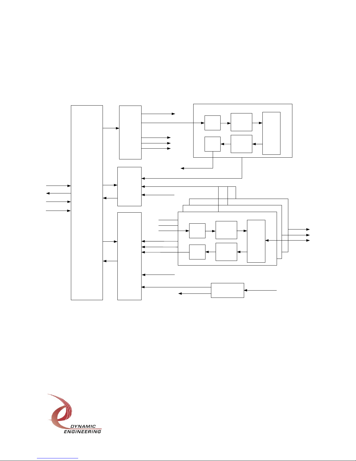
Power Circuits
Monitors & Power in range LEDs
P12V
CPLD Paralle l
FPGA Loader
PERp/n0
16 bit – 90ns
FLASH
JTAG
Header
32MHz
OSC
PETp/n0
Lattice ECP3 FPGA
CFG & TEST
P5VGOO D
Parallel CFG & Data
USER DIP Switch Input s
TDO
PCIe REFCLK +/-
M12V P5V
3.3V 1.2V
CFG & TEST
DIP Switch
USER
DIP Switch
USER LED [7:0]
x1
PCI
Express
Edge
Fingers
Connector
TDI
TDI
TDO
Lattice ECP3 FPGA
PCI
Express
Core
PERST#
IP0
Interface
IP0
IP0 ACK* Activity LED
``
Carrier
IP0 Logic
Connector
SMT
3.3V – 5V
Level
Shifter
``
HDR_50
IP0
RT Angle
Header
With
Ejectors
IP0
Carrier
IO
Connector
SMT
IP1
Interface
IP1
IP1 ACK* Activity LED
``
Carrier
IP1 Logic
Connector
SMT
3.3V – 5V
Level
Shifter
``
HDR_50
IP1
Vertical
Header
IP1
Carrier
IO
Connector
SMT
IP2
Interface
IP2
IP2 ACK* Activity LED
``
Carrier
IP2 Logic
Connector
SMT
3.3V – 5V
Level
Shifter
``
HDR_50
IP2
Vertical
Header
IP2
Carrier
IO
Connector
SMT
The PCIeIP Architecture is the foundation for all the devices in the PCIeIP Carrier
Series. The PCIe3IP Block Diagram (Figure 1) and PCIe3IP FPGA Block Diagram
(Figure 2) illustrate a 3IP channel design using the PCIeIP Architecture. To create the
PCIe5IP two additional IP channels (IP3 & IP4 – not shown) are implemented. To create
the VPX2IP the IP2 channel is removed.
PCIe3IP Block Diagram
Figure 1 PCIe3IP Block Diagram
Embedded Solutions Page 14 of 71
Page 15
PERp/n0
PETp/n0
REFCLK +/-
Credits
Available
Unsupporte d
Request
Packet G enerator
Credits
Processed
Receive
FIFO
&
Packet
Router
PCI Express
Core
PERST#
TX Arbite r
& Packet
Transmitter
Credit
processor
IP1 Rx Packet
IP2 Rx Packet
Un-support Request
Un-support Request
Rx Packet
Interface
IP1 Channel
IP2 Channel
Read/Wr ite
Packet
Processor
Receive
Packet
FIFO
READ
Completion
Packet
Generator
Transmit
Packet
FIFO
IP0 Channel
IP
Data Path
State
Machines
&
Logic
Register Rx Packet
IP0 Rx Packet
Tx Packet
Interface
Tx RDY
Read/Wr ite
Packet
Processor
Receive
Packet
FIFO
READ
Completion
Packet
Generator
Transmit
Packet
FIFO
Register Channel
PICe3IP
Registers
IP1 Rx Packet
IP0 Rx Packet
IP2 Rx Packet
IP1 Tx Packet
IP2 Tx Packet
IP0 Tx Packet
Register Tx Packet
Register Tx Packet
Un-support Request Tx Packet
Register Credit
IP0/IP1/IP2 Credits
UR Credit
UR Credit
IP2
IP1
IP0
IP Interfaces
PCIe3IP FPGA Block Diagram
Figure 2 PCIe3IP FPGA Block diagram
Embedded Solutions Page 15 of 71
Page 16

Theory of Operation
PCIeIP functions as a bridge between PCI Express and IP bus devices that adhere to
their respective specifications. Since there are no additional PCIe virtual buses or PCIe
ports downstream from the PCIeIP’s PCI Express port, the PCIeIP is defined to be a
PCIe Endpoint. As an Endpoint the PCIeIP is downstream from the Host/Root Complex
which detects it and configures it during the enumeration process using PCIe
configuration read and write packets. The VPX2IP/PCIe3IP requests a total of 32MB
and the PCIe5IP requests 64MB from the Host who provides the requested memory
space via BAR0. Each IP's ID, IO, INT, and MEM spaces are mapped inside the
32/64MB space. When the PCIe Host transmits either a memory read or write packet
which contains an address within the PCIeIP’s BAR0 it is routed to either the PCIeIP
register block, or one of the IP’s to be further decoded to generate an ID, IO, INT, or
MEM space IP access.
The VPX2IP/PCIe3IP/PCIe5IP handles all accesses within its 32/64 MB of space.
Writes to reserved registers or memory are dropped. For reserved register reads,
0x0000_0000 is returned. For reads of undefined memory spaces, 0xFFFF_FFFF is
returned. In all cases credits are updated.
If a packet is received with an address outside the PCIeIP’s BAR0 space it is discarded,
credits are updated, and an unsupported request PCIe packet is returned to complete
the transaction.
PCIeIP uses a Lattice semiconductor ECP3 Family FPGA and utilizes Lattice’s PCI
Express Endpoint Core IP which is compliant to PCI-SIG PCI Express 1.1 Base
Specifications. The core handles the PCIe Physical and Data Link Layer requirements
and provides an extensive interface which the PCIeIP interacts with to receive or
transmit Transaction Layer Packets (TLPs) and communicate and/or update available
flow control credits.
All Transaction Layer Packets coming from the PCIe Core that are within BAR0 space
are written into a receive packet FIFO. Upon detecting a packet is in the receive FIFO it
is immediately read out, routed and written into the target IP’s or registers receive FIFO.
The FIFO’s are sized and PCIeIP advertises credits such that no access packet has to
wait behind a different IP channels access packet, as such this creates a Non-blocking
IP FIFO architecture. However, since the IP interfaces run much slower than the rate at
which incoming receive FIFO Packets can be received, packets can back up inside a
particular IP’s receive FIFO, but will never backup into the main receive FIFO.
Embedded Solutions Page 16 of 71
Page 17

For example if 100 reads are in one IP’s receive FIFO and a new read is received for a
different IP, it will be routed into that IP’s receive FIFO.
The header credits are set to the maximum allowed by the PCIe core, which is 127, so
up to 127 combined IP read and write requests may be pending at any one time inside
the PCIeIP.
Once a register or IP access has completed processing a write or read, the appropriate
credit updates will be accumulated and sent to the core which will create Flow Control
DLL packet(s) to inform/update the Host that more space/credit is available inside the
PCIeIP. For the VPX2IP/PCIe3IP/PCIe5IP there are three/four/six possible read targets
and/or sources for read completion packets, they are: IP[1:0]/IP[2:0]/IP[4:0], and a
register access. When the read target has assembled the read completion packet it
stores it in its transmit FIFO as it must arbitrate for and then write the completion into
the transmit packet port of the PCIe core. The transmit packet arbiter is a round robin
arbiter. The transmit packet port won’t grant access until the core informs it is ready to
receive a packet.
Embedded Solutions Page 17 of 71
Page 18

Programming
Function
Offset
Size
Registers – IP[2:0]
0x000 – 0x3FF
1K Bytes
ID Space – IP0
0x400 to 0x47F
128 Bytes
ID Space – IP1
0x480 to 0x4FF
128 Bytes
Reserved
0x500 to 0x7FF
768 Bytes
IO Space – IP0
0x800 to 0x87F
128 Bytes
IO Space – IP1
0x880 to 0x8FF
128 Bytes
Reserved
0x900 to 0xBFF
768 Bytes
INT Space – IP0
0xC00 to 0xC7F
128 Bytes
INT Space – IP1
0xC80 to 0xCFF
128 Bytes
Reserved
0xD00 to 0xFFF
768 Bytes
Reserved
0x1000 to 0x7F_FFFF
8 MB-4KB
MEM Space – IP0
0x080_0000 to 0x0FF_FFFF
8 MB
MEM Space – IP1
0x100_0000 to 0x17F_FFFF
8 MB
Reserved
0x180_0000 to 0x1FF_FFFF
8 MB
PCIeIP is tested in a Windows environment. We use the Dynamic Engineering Driver to
do the low level accesses to the hardware. We use MS Visual C++ in conjunction with
the driver to write our test software. Please consider purchasing the engineering kit for
the VPX2IP, PCIe3IP or PCIe5IP; the software kit includes our test suite. In addition
Linux and VxWorks drivers and reference suites are available.
The drivers take care of discovery and the UserAp allows the client to select which
installed board is selected for use.
If you are writing your own driver it is suggested to get the engineering kit and the Linux
version of the SW. Usually the code defines and perhaps some of the code can be
reused in your effort.
VPX2IP Address Map
Figure 3 VPX2IP Base Address Map
Embedded Solutions Page 18 of 71
Page 19

Function
Offset
Size
Registers – IP[2:0]
0x000 – 0x3FF
1K Bytes
ID Space – IP0
0x400 to 0x47F
128 Bytes
ID Space – IP1
0x480 to 0x4FF
128 Bytes
ID Space – IP2
0x500 to 0x57F
128 Bytes
Reserved
0x580 to 0x7FF
640 Bytes
IO Space – IP0
0x800 to 0x87F
128 Bytes
IO Space – IP1
0x880 to 0x8FF
128 Bytes
IO Space – IP2
0x900 to 0x97F
128 Bytes
Reserved
0x980 to 0xBFF
640 Bytes
INT Space – IP0
0xC00 to 0xC7F
128 Bytes
INT Space – IP1
0xC80 to 0xCFF
128 Bytes
INT Space – IP2
0xD00 to 0xD7F
128 Bytes
Reserved
0xD80 to 0xFFF
640 Bytes
Reserved
0x1000 to 0x7F_FFFF
8 MB-4KB
MEM Space – IP0
0x080_0000 to 0x0FF_FFFF
8 MB
MEM Space – IP1
0x100_0000 to 0x17F_FFFF
8 MB
MEM Space – IP2
0x180_0000 to 0x1FF_FFFF
8 MB
PCIe3IP Address Map
Figure 4 PCIe3IP Base Address Map
Embedded Solutions Page 19 of 71
Page 20

Function
Offset
Size
Registers – IP[2:0]
0x000 – 0x3FF
1K Bytes
ID Space – IP0
0x400 to 0x47F
128 Bytes
ID Space – IP1
0x480 to 0x4FF
128 Bytes
ID Space – IP2
0x500 to 0x57F
128 Bytes
ID Space – IP3
0x580 to 0x5FF
128 Bytes
ID Space – IP4
0x600 to 0x67F
128 Bytes
Reserved
0x680 to 0x7FF
384 Bytes
IO Space – IP0
0x800 to 0x87F
128 Bytes
IO Space – IP1
0x880 to 0x8FF
128 Bytes
IO Space – IP2
0x900 to 0x97F
128 Bytes
IO Space – IP3
0x980 to 0x9FF
128 Bytes
IO Space – IP4
0xA00 to 0xA7F
128 Bytes
Reserved
0xA80 to 0xBFF
384 Bytes
INT Space – IP0
0xC00 to 0xC7F
128 Bytes
INT Space – IP1
0xC80 to 0xCFF
128 Bytes
INT Space – IP2
0xD00 to 0xD7F
128 Bytes
INT Space – IP3
0xD80 to 0xDFF
128 Bytes
INT Space – IP4
0xE00 to 0xE7F
128 Bytes
Reserved
0xE80 to 0xFFF
384 Bytes
Reserved
0x1000 to 0x7F_FFFF
8 MB-4KB
MEM Space – IP0
0x080_0000 to 0x0FF_FFFF
8 MB
MEM Space – IP1
0x100_0000 to 0x17F_FFFF
8 MB
MEM Space – IP2
0x180_0000 to 0x1FF_FFFF
8 MB
MEM Space – IP3
0x200_0000 to 0x27F_FFFF
8 MB
MEM Space – IP4
0x280_0000 to 0x2FF_FFFF
8 MB
Reserved
0x300_0000 to 0x3FF_FFFF
16 MB
PCIe5IP Address Map
Figure 5 PCIe5IP Base Address Map
Embedded Solutions Page 20 of 71
Page 21

The address maps provided are for the local decoding performed within PCIeIP. The
addresses are all offsets from a base address. The base address, BAR0 is provided by
the host in which the PCIeIP is installed.
The host system will enumerate to find the assets installed during power-on initialization
- The PCIe3IP Vendor ID = 0xDCBA and Device ID = 0x0051.
- The PCIe5IP Vendor ID = 0xDCBA and Device ID = 0x005C.
- The VPX2IP Vendor ID = 0xDCBA and Device ID = 0x0060.
Third party utilities can be useful to see how your system Memory Map is configured.
The interrupt level expected and style is also set in the registry. Dynamic Engineering
recommends using the Dynamic Engineering Driver to take care of initialization and
device registration.
Once the initialization process has occurred and the system has assigned an address
range to the PCIeIP card, the software will need to determine what the address space
is. We refer to this address as base in our software.
The next step is to initialize the PCIeIP by configuring the IP(s) control and interrupt
registers. Optionally registers such as the Switch and LED control may also be
configured at this point.
Dynamic Drivers provide all of the above functionality and a generic IP driver for use
when a specific IP driver is not available for a particular IP.
Dynamic Engineering drivers are supported with “UserAp”. UserAp provides a miniapplication to perform tasks on the IP and PCIeIP. UserAp is provided with the source
code to allow our clients to have a running start at integration. The UserAp code is
developed to do ATP testing on the hardware and is complete from a feature
development point of view. UserAp has functionality in main.c to call the driver and get
the handle to the IP. In addition the functionality to discover multiple cards on multiple
carriers is provided. The handle is used along with the specific offsets for the carrier or
IP to access the hardware.
The user switch can be used to deterministically select the intended IP module when
multiple carriers with multiple modules are in a system. Setting the switches to different
known values and reading the switch values from the carriers, then remapping the
handles for the carriers can provide an automatic mechanism to be sure your
application software is communicating with the correct IP when multiple IP’s of the same
type are available within the system.
Embedded Solutions Page 21 of 71
Page 22

PCIeIP Resets, Clocks, & Bus Error
PCI Express Reset (PERST#) summary
There are two types of resets in PCIe, both of which are supported by the PCIeIP, they
are:
Fundamental Reset (cold or warm) – assertion of PERST#
o Cold - Power applied to a cold (non-powered) system.
o Warm – Power is up/good before & during assertion of PERST#.
Hot Reset – TS1 Ordered-Sets sent with bit [0] of symbol 5 asserted for 2ms.
Per the PCIe specification:
The minimum PERST# assertion time is 100ms from the time power is stable.
o In order to be configured and ready for enumeration before PERST# is de-
asserted PCIeIP downloads the FPGA configuration file from a parallel
Flash.
PERST# signal is asserted and de-asserted asynchronously.
IP Reset* Summary
Reset* (IPx_RESETN) signal rules from Vita Spec:
When asserted, Reset* must be asserted for a minimum of 200ms, there is no
maximum.
Can be asserted asynchronously, and must be de-asserted synchronously.
+5V must be monitored and reset asserted if power falls below minimum spec
Reset* is the logical OR of Power monitoring reset and the system reset.
IP module documents must clearly state the time needed from Reset* de-
assertion until the IP module is initialized.
When Reset* is asserted IP’s must terminate any cycle, interrupts, DMA requests
or future requests.
The PCIeIP supports all Carrier card rules for Reset*.
Embedded Solutions Page 22 of 71
Page 23

PCIeIP Reset* functional behavior
PCI Express PERST# assertion response - Each IP’s Reset* is asserted as long as the
PERST# is asserted. Once PERST# is de-asserted each channel starts its own 256
millisecond counter, which when it expires causes that channels Reset* to be
synchronously de-asserted relative to its clock.
User Control bit response - Each IP channel’s Reset* in the PCIeIP can be asserted
independently. The PCIeIP provides the following three register bits in each IPx’s
control0 register (i.e. offset 0x80 for IP0):
Reset IP - IPx Control0 Register bit [16] – Reset* is driven low as long this bit is
set to 1, upon writing this bit back to zero Reset* is de-asserted. Meeting the
minimum assertion time of the IP is the responsibility of the software.
Reset IP and channel - IPx Control0 Register bit [17] – Reset* is driven low as
long this bit is set to 1, upon writing this bit back to zero Reset* is de-asserted
after the expiration of that channels 256 millisecond reset counter to ensure
Reset* meets the 200ms minimum assertion time. Assertion of this bit also resets
all channel related logic and FIFO, for predictable behavior assertion of this bit
should occur after R/W requests to the channel have been completed and no
further accesses are submitted until the Reset* pin has been de-asserted.
IP Reset pin status - IPx Control0 Register bit [18] – Provides real time value of
the IP’s Reset* pin state. If 0 the IP Reset* pin is de-asserted (1), if 1 the IP
Reset* pin is asserted (0).
P5VGOOD pin response – If the PCIeIP voltage monitoring circuit detects 5 volt power
is out of specification it asserts the P5VGOOD pin to 0. Since the P5VGOOD pin
assertion is asynchronous the PCIeIP synchronizes it and ensures it has been asserted
for at least two clock cycles before detecting it as asserted. Internally if the P5VGOOD
pin value is detected to be 0, the PCIeIP will assert each channels Reset* for the
duration P5VGOOD is 0 + 256 milliseconds. The PCIeIP will also set each channels
Force/P5VGOODn Interrupt – see Interrupt section for details. P5VGOOD pin = 0 would
not be expected even under extreme operating conditions.
Since the PCI Express interface and register logic inside the PCIeIP are clocked
independent of the IP logic the PCIeIP can be configured by the software between the
time PERST# de-asserts and Reset* de-asserts. Accesses to each IP should be
delayed until after the IP Reset* timers have expired 256 milliseconds after PERST# deassertion.
Asserting the Reset IP - IPx Control0 Register bit [16] has no effect the channels IP
clock frequency as set by the Clock SEL bit. Assertion of the Reset IP and channel - IPx
Control0 Register bit [17], or if P5VGOOD is 0, will force the Clock SEL for that channel
to be 0 (8MHz) for the duration of the assertion plus 256ms at which time the frequency
will revert back to 32MHz if the Clock SEL bit is set to 1.
Embedded Solutions Page 23 of 71
Page 24

PCIeIP Clocks
Each IP channel on the PCIeIP has its own independent clock (CLK). IP CLK’s are held
low until PERST# is de-asserted. Upon de-assertion of PERST# each IP CLK becomes
active and runs at 8MHz. Each IP channel’s CLK frequency can be set independently to
32MHz or back to 8MHz at any time without restriction by setting or clearing that
channels Clock SEL bit - IPx Control0 Register bit [8].
Each channel’s CLK can optionally be turned off and set to a steady state of high
(disabled) if the user knows that the channel will not be used and/or has EMI concerns.
To disable or enable an IP channel’s CLK users may set or clear that channels Clock
disable bit - IPx Control0 Register bit [9]. As long as there are no transfers in process
when the clock is disabled it may be re-enable and the channel will process read write
requests as normal. Warning: If the channel is disabled and reads/writes continue to be
sent to that channel the FIFO’s in the PCIeIP will back up, credits won’t be replenished,
and the PCIeIP will become congested and unable to communicate with
enabled/working IP’s.
Each IP CLK clock edge is relative to the 32MHz oscillator clock on the PCIeIP board.
In order to reduce SSO (Simultaneous Switching Outputs) i.e. switching noise, The
PCIeIP has an IP Clock Phase Stepper circuit which phase shifts IP1’s clock rising edge
by 8ns, and IP2’s clock rising edge by 16ns relative to IP0’s clock rising edge. For the
PCIe5IP, IP3/IP4’s clock is in phase with IP0/IP1’s clock.
Bus Error processing
In regards to Bus Error the vita spec states the following:
In the 8 MHz Data Transfer Cycle Details section – “There is no explicit provision
for cycle timeout. Even if an IP Module supports a specific select line it is not
required to always assert ACK* … However the IP Module literature must clearly
state access time, or “wait states.” … RECOMMENDATION 10-26: IP Modules’
maximum ACK* time should generally be not be more than a few microseconds.”
In the 32 MHz Operation section – “A maximum number of permitted wait states
by an IP Module at 32 MHz is 127 clock cycles.”
Each IP channel in the PCIeIP has its own logic to monitor how long the channel waits
for ACK* before terminating the cycle as a Bus Error. The PCIeIP provides some
flexibility for users to choose how long the wait should be using the Bus Error timeout
select (IPx Control0 Register bit [12]). Its settings are:
0 = 127 IP Clocks – 4us @ 32MHz or 63 IP Clocks - 8us @ 8MHz (0 is the
default)
1 = 255 IP Clocks – 8us @ 32MHz or 127 IP Clocks - 16us @ 8MHz
Embedded Solutions Page 24 of 71
Page 25

A Bus Error event occurs when the PCIeIP initiates an R/W access to an IP and the IP
doesn’t assert its ACK* within the predefined number of IP clocks. The number of clocks
the PCIeIP waits is determined by the frequency of operation and the setting of the Bus
Error timeout select bit. Upon the occurrence of a Bus Error that IP channel sets its Bus
Error Interrupt bit (IPx ISR bit [2] = 1) and an interrupt can be generated.
In normal operation the PCIeIP receives PCI Express packets to write or read up to
64bits on the IP bus. Byte enables are also received in the packet which the PCIeIP
uses to determine if a byte, word, Dword, two Dword, or four Dword R/W transaction will
be generated on the IP bus. If ACK* is not received for a write, the write transaction is
terminated, data is discarded and credits are updated accordingly.
If ACK* is not received for a read, then depending upon the transfer size and/or byte
enables a read will return different completion data. For a 64bit transfer, the PCIeIP
generates two separate 32bit accesses, as such the data returned when ACK* isn’t
provided is the same as when an ACK* isn’t provided during two 32bit transfers back to
back. A 32bit transfer causes the PICeIP to do two 16bit IP transfers, if ACK* isn’t
received for the first 16bit IP transaction 0xFFFF_FFFF will be provided and the second
16bit IP transaction will not be generated on the IP bus. If the ACK* is received for the
first IP transaction, but not the second, the read will have 0xFFFF in the upper word and
valid data in the lower word of the 32 bit PCIe read completion data field.
For non 32bit reads where an ACK* does not occur 0xFFFF will be returned for a Dword
access that has a valid byte enable(s). A word in the 32bit completion data field where
the byte enables are not asserted will have 0x0000 in them regardless if there is a Bus
Error or not. Therefore, the completion data returned depends upon the each IP
transfer’s byte enables and which transfer the IP doesn’t provide an ACK*.
When a Bus Error occurs the IP state machines will return to their idle state so that they
are able to process the next transaction. For all possible read combinations with bus
errors credits are updated accordingly.
Bus Error interrupts can, and are used during initialization to scan the IPx ports to detect
the presence of an IPx installed in a slot. Typically a driver will do a 32bit (or 16bit)
access of the slot’s/IP’s ID space, and if it detects either 0xFFFF_FFFF (or 0xFFFF) it
knows an IP is not installed in that slot. Once a system is initialized and running a Bus
Error interrupt is normally considered a serious system error.
Embedded Solutions Page 25 of 71
Page 26

IP Channel Transfer Activity Monitor and Logic
To provide the ability to check an IP channel’s transfer activity status, health, or to
enable sequenced IP transfers the PCIeIP contains an IPx Channel Transfer Monitor
Register (IPx CTM) for each IP channel. Below is a summary the IPx CTM register bits
and logical behavior:
An IPx Channel Busy (IPx CTM bit [28]) indicator – This register bit provides a
way to ascertain the activity status of that channel. When the IPx Channel Busy
status indicator is 0 it indicates there are no transfers in process or pending for
that channel. When the IPx Channel Busy status indicator is 1 it indicates at least
one transfer is still pending in the channel’s FIFO or the IP interface is still
processing a transfer. The IPx Channel Busy status changes from busy to not
busy [1 to 0] when the respective channel FIFO is empty, and all IP interface
write/read cycles have completed (which can be several ACK cycles when
performing multi-word accesses). Note: In the case of a Read Instruction, the
busy signal may go to the not busy state before the read data reaches the CPU
since arbitration and core processing may not have completed.
A 16 bit IPx ACK* counter whose count can be read by reading that channels IPx
ACK* count (IPx CTM bits [15:0]) to determine if all the required ACK*’s for the
cycles submitted to that IP have been received. This counter is enabled when
both the ACK* Count Enable (IPx Control0 register bit [13]) and IPx ACK*
Counter Clear#/Enable (IPxCTM bit [24]) are enabled (set to 1).
An IPx ACK* Counter Clear#/Enable (IPx CTM bit [24]) register bit which clears
and holds the ACK* Counter to 0x0000h when 0. When 1 it enables the ACK*
counter to count ACK*’s.
The IPx Channel Busy indicator and ACK* counter logic are independent of each other.
Users may use either or both together if they choose. For accurate transfer monitoring
that all transfers have completed it is recommend that the IPx counter and IPx ACK*
Counter Clear#/Enable logic be used.
Embedded Solutions Page 26 of 71
Page 27

One possible usage example would be as follows:
A system engineer wants to issue and ensure completion of 20 Dword transfers
(composed of Reads and Writes) to IP0, then do and ensure completion of 20 Dword
transfers to IP1, then do and ensure completion of 20 Dword transfers to IP2. To do this
with the PCIeIP the engineer could do the following.
1) Enable each channels ACK* counter by setting each IP’s ACK* Count Enable
(IPx Control0 register bit [13]) bit = 1.
2) Ensure each channels IP counter is clear, by clearing IP0, IP1, and IP2 ACK*
Clear#/Enable bit by writing each channels IPx CTM bit [24] register bit = 0.
3) Instruct the software to stop issuing IP channel Read/Writes and then read each
IPx Channel Busy (IPx CTM bit [28]) indicator bit until each bit is 0.
4) Enable IP0, IP1, and IP2 ACK* counters to count their channel’s ACK*’s by
writing each channels IPx’s Clear#/Enable (IPx CTM bit [24]) register bit = 1.
5) Submit the 20 Dword transfers to IP0, then read IP0’s ACK* count value. When
the ACK* count is equal to 40 decimal all ACK* for the 20 Dword IP transfers
have been received.
6) Repeat 4) for IP1 then IP2.
Embedded Solutions Page 27 of 71
Page 28

PCIeIP Interrupts
This sections purpose is to summarize the PCIeIP Interrupts, Interrupt registers,
programmable features usage, and behavior. Here’s a brief description of what’s
covered:
o Summary of PCIe spec. Interrupt configuration registers
o Summary of Interrupt registers/bits contained in the PCIeIP.
o Summary of the PCIeIP’s Interrupt specific registers and bits.
o Detailed description of PCIeIP’s Interrupt functionality and features.
o Detailed summary of the PCIeIP’s Interrupt specific registers and bits.
PCIeIP PCI Express Interrupt Registers Summary
PCI Express has two possible types of Interrupt packets that can be generated, they
are:
INTx# – Legacy PCI Interrupt virtualization packets.
MSI – Message Signal Interrupt packets.
PCIeIP supports both MSI and INTx# interrupt packet generation.
There are eight PCI Express configuration (type 0) registers contained in the PCIeIP
which are involved in the generation of interrupt packets.
The next section summarizes the four registers with INTx# related bits, followed by a
section that summarizes the four registers with MSI related bits. The summary of these
registers is provided to ease users understanding of PCI Express Interrupts. Users need
not be concerned with setting or using the register values written by the host as they are
used by the PCIeIP PCI Express core when generating INTx# or MSI PCI Express
packets.
Embedded Solutions Page 28 of 71
Page 29

PCIeIP PCI Express INTx# Interrupt Configuration Registers Summary
Command Register (offset 0x04)
Interrupt Disable (bit [10]) R/W, 0 = INTx# enabled (default), 1 = INTx# disabled.
Status Register (offset 0x06)
Interrupt Status (bit [3]) RO, 0 = no Interrupt pending (default), 1 = Interrupt
pending. Only valid in INTx# Mode. Disabled, always zero in MSI mode.
Capabilities List (bit [4]) RO, 0 no capabilities registers, 1 = capabilities registers
exist. This bit is hardwired to 1 in PCIeIP - MSI registers are capability registers.
Interrupt Line Register (offset 0x3C)
Interrupt Line [7:0] R/W register written by the Host to distinguish device
interrupt.
Interrupt Pin Register (offset 0x3D)
Interrupt Pin [7:0] RO register, hardwired to 0x01 in PCIeIP to indicate INTA#.
PCIeIP PCI Express MSI Interrupt Configuration Registers Summary
Message Control Register (offset 0x72)
MSI Enable (bit [0]) R/W, 0 = MSI’s disabled (default), 1 = MSI’s enabled.
Multiple Message Capable (bits [3:1]) RO, 0x0 = PCIeIP requests 1 MSI.
Multiple Message Enable (bits [6:4]) R/W, 0x0 (default) Host writes to allocate
MSI’s.
64 bit Address Capable (bit [7]) RO, 1 = PCIeIP is 64 bit MSI address capable.
Message Address Register (offset 0x74)
Message Address (bits [31:2]) R/W, Host provides - bits [31:2] of D-Word
aligned MSI address.
Message Upper Address Register (offset 0x78)
Message Address (bits [63:32]) R/W, Host provides - upper 32bits for 64bit MSI
addressing.
Message Data Register (offset 0x7C)
Message Data (bits [15:0]) R/W, Host provides - value used to distinguish
PCIeIP interrupt.
Embedded Solutions Page 29 of 71
Page 30

PCIeIP Interrupts and Registers Summary
For each IP channel there are four possible interrupt sources.
IPx Force/P5VGOODn Interrupt – Dual source, either user programmable
interrupt via register bit or interrupt set due to detection of the 5 volt power
source being out of range.
IPx Bus Error Interrupt – Occurs when an IPx does not respond to an access.
IPx IntReq[1:0]* Interrupts – Occurs when an IPx asserts one of its IntReq[1:0]*
pins.
PCIeIP has two “global” interrupt registers related to all IP’s and two registers for each
IP, registers specific to an IP are prefixed with IPx. Details of each register mentioned in
this section can be found in section 4. The offsets noted below are relative to BAR0.
Here’s a brief summary of each register:
Interrupt Status Register (ISR) at offset 0x008 – Contains all PCIeIP Interrupt
bits, each bit in this register can cause the generation of an Interrupt packet.
Interrupt Control Register (ICR) at offset 0x00C – Contains bits that control the
timing of when an interrupt packet is generated and sent to the Host.
IPx Interrupt Status Register (IPx ISR) – Bits in these registers either contain or
reflect the value of the Interrupt source that can cause the generation of an
Interrupt packet if it is allowed to progress to the ISR (see spec for offsets, i.e.
IP0 ISR offset is 0x088)
IPx Interrupt Control Register (IPx ICR) – This register contains the Enable/Mask
bits for each IPx Interrupt. Mask bits control whether or not an interrupt
progresses to the ISR. The IPx ICR also contains a Level/Edge Interrupt control
bit for each IPx Interrupt. A Level/Edge control bit changes the interrupt packet
generation behavior for that interrupt. In Level mode multiple interrupts may be
sent to the Host per a single interrupt, in Edge mode only one interrupt will be
sent per interrupt assertion. (see spec for offsets, i.e. IP0 ICR offset is 0x08C)
Embedded Solutions Page 30 of 71
Page 31

PCIeIP Interrupt Functional Operation
The descriptions of the PCIeIP interrupt behavior to follow refer to the PCIe compliant
configuration registers and PCIeIP specific Interrupt registers both of which were
summarized in sections 1.0 and 2.0. This was done for the convenience of the reader
and should be sufficient for understanding the remainder of this document. For specific
details of PCIeIP Interrupt register bits/functions please refer to section 4.0. For PCI
Configuration register details please refer to the relevant PCI and/or PCIe specification.
When PCIeIP comes out of reset it is in INTA# mode as both the Interrupt Disable and
MSI Enable bits are 0 by default. It is up to the Host to determine if all devices in the
system can support MSI before configuring the system to use MSI Interrupts. This
section will first describe how PCIeIP INTA# virtualized signaling works then describe
the setup, functional, and behavioral differences for MSI Interrupts.
PCIeIP INTA# Interrupt Functional Operation
Each IP channel has 4 possible interrupt sources: Force/P5VGOODn, Bus Error, and
IntReq[1:0]*. The state of a channels interrupt sources are in its IPx ISR bits [3:0]. When
asserted these bits are true high. Each channel also has an IPx ICR register which
contains an Interrupt enable bit for each source interrupt. When disabled the interrupt
source is Masked (i.e. blocked) from generating an interrupt to the Host, each Interrupt
Enable/Mask bit is 0 by default (0 = disabled/masked). The Host may enable any IP
channel source interrupt independently by setting any of the IPx ICR [3:0] bits = 1.
If an Interrupt source is asserted and enabled (not Masked) it will be registered in the
ISR (0x008). The ISR has a register bit for every possible interrupt. When an ISR bit is
set it causes PCIeIP to generate and send a PCI Express INTA# Message packet that
contains an Assert INTA message code to the Host. Since PCIeIP only has one
interrupt for multiple possible interrupt sources the Host will have to read the ISR to
determine which Interrupt or Interrupts are asserted. To clear an Interrupt/bit the Host
must Write 1 to Clear (W1C) the interrupt bit in the ISR. When the Host executes a W1C
of an ISR bit or bits, the bit(s) will be cleared and PCIeIP will generate and send another
INTA# Message packet, this time the packet will contain a Deassert_INTA message
code.
Once a W1C of any ISR bit occurs the PCIeIP will wait until the Interrupt de-assert timer
expires before checking to see if an ISR bit is set. If an ISR bit is set when or after the
timer expires PCIeIP will generate another assert INTA# packet.
Embedded Solutions Page 31 of 71
Page 32

PCIeIP Interrupt Level/Edge Functionality
PCIeIP IPx ICR [11:8] Level/Edge bits individually configure each of a channels four IP
interrupts to be either Level or Edge. In Level mode, if an IPx ISR bit (i.e. source) is
asserted and enabled when a W1C for that ISR bit occurs, it triggers the de-assert
INTA# packet to be generated. Since the source is still active the interrupt will remain
set in the ISR. Another INTA# assert packet will be generated once the de-assert timer
expires. In other words the PCIeIP can generate and send multiple interrupt assert
packets to the Host for a single interrupt source assertion. This will continue as long as
the interrupt source (in IPx ISR) remains asserted and enabled regardless of when or
how many W1C of the ISR occurs. If the source in the IPx ISR is cleared before the
W1C of the ISR bit it will not be the cause of an additional Interrupt assertion when the
de-assertion timer expires (unless it is reasserted before the timer expires). ICR bits
[2:0] select the Interrupt de-assertion time which ranges from 96 nanoseconds to 33
microseconds. In most cases the edge mode will be used. Level mode is useful when
a device needs to be read or loaded whenever above/below a certain level [FIFO etc.]
Just because the SW loads data does not mean the condition has been removed.
In Edge Mode, when an interrupt source is set and enabled, its respective ISR bit will be
set and an INTA# interrupt assert packet will be generated and sent to the Host. When
the Host performs a W1C of that ISR bit it will clear the ISR bit and PCIeIP will send a
de-assert INTA# packet to the Host. That ISR bit will remain clear and no further INTA#
packets will be generated [due to that specific bit] until the source interrupt is deasserted and reasserted. This means that only one Interrupt will be send to the Host per
assertion of the source interrupt regardless of how long the source interrupt is asserted.
In this mode the interrupt can be detected, cleared, and a flag set in SW to cause the
higher level application to take action which will result in clearing the interrupt. During
this sequence additional interrupts are blocked due to the requirement for the interrupt
source to be cleared before it can be set again.
Embedded Solutions Page 32 of 71
Page 33

PCIeIP Interrupt Aggregation
PCIeIP contains an Interrupt Aggregation timer and logic that enables the user to
program the rate at which an interrupt can be generated. The Interrupt Aggregation
enable bit (ICR bit [13]) is =0 off/disabled by default, when enabled (ICR bit [13] = 1) the
Interrupt Aggregation timer starts counting and provides a pulse when the user selected
time delay is reached. ICR bits [11:8] select the Interrupt Aggregation time which ranges
from 32 microseconds to 1 second. When the Interrupt Aggregation pulse occurs it is
used to generate an interrupt assertion packet if an Interrupt is set in the ISR. Once the
pulse is generated the Aggregation Logic timer is reset and starts counting again until
the Aggregation delay is reached and a pulse is generated again. This fixed cyclical
timing (or pace) repeats until disabled. If your system has multiple interrupt sources
and the interrupts can be processed with some delay, using the timer will group the
interrupts together and reduce interrupt processing. The programmable time allows the
user to tune the accumulation time to match system requirements.
PCIeIP Interrupt Timing, Behavior, and W1C
The number of interrupt sources that can cause PCIeIP to generate an interrupt packet
to the Host depends upon how many IP’s are connected. Since there are 4 sources per
IP the number of possible interrupt sources = 4 x IPs. All the interrupt sources are
synchronized internally before being used and setting their respective ISR bits.
However, only under controlled circumstances can one accurately predict when
interrupt sources will assert or de-assert. In normal (non-controlled) operating
environments interrupts may assert on any clock cycle, including before, after, or even
on the same clock cycle of key interrupt related events such as a read of the ISR or a
W1C cycle. For example you may read the ISR and not “see” an Interrupt set, then read
it immediately again and “see” several interrupts set. You may also process an interrupt,
W1C it then read the ISR to “see” the same interrupt set again.
Because PCIeIP handles interrupts internally in a synchronous fashion and registers
them in the ISR the system software only needs to follow one simple rule to avoid
“losing” interrupts.
Interrupt W1C Rule: Only Write 1 to Clear (W1C) the ISR bits (i.e. interrupts) that
you’ve processed.
The reason for this is that new/additional interrupts may be asserted and logged in the
ISR since the original reading of the ISR so if the software were to do a W1C of all the
ISR bits the new/additional interrupt(s) could be lost.
Embedded Solutions Page 33 of 71
Page 34

PCIeIP IP Interrupts
When asserted each of the IP interrupt sources: Force/P5VGOODn, Bus Error, and
IntReq[1:0]* if enabled will set their respective bit in the ISR. The current status of the
source value can be read at any time by reading the respective IP’s IPx ISR. If the
source “goes away” the respective ISR bit will remain set until a W1C of the ISR bit is
executed. Below are additional details about each IPx Interrupt source register and/or
signal.
IPx Force/P5VGOODn Interrupt – The Force/P5VGOODn Interrupt has two possible
sources, they are:
1) The Force Interrupt source bit (IPx ISR bit [3]) is a register bit under user control
and may be read or written at any time. This bits purpose is to provide a way for
the user to assert/de-assert an interrupt in a controlled fashion for development
or design purposes. Notes: Since all incoming register R/W packets flow into a
register accesses FIFO they are processed in the order they are received,
therefore if there are other register accesses ahead of the Force interrupt R/W, it
will be delayed proportionately.
2) Even under extreme operation conditions the P5VGOOD pin should be at a logic
1, however if the PCIeIP voltage monitoring circuit detects 5 volt power is out of
specification it asserts the P5VGOOD pin to 0. Internally PCIeIP synchronizes
the P5VGOOD pin value, ensures it has been asserted for at least two clock
cycles, and inverts its value to create the P5VGOODn interrupt signal. When
P5VGOODn goes high it sets each IPx’s Force/P5VGOODn bit in the ISR
register, these bits will stay set until cleared with a W1C. The IPx
Force/P5VGOOD bit in the IPx ISR reflects the inverted value of P5VGOOD pin,
as such it is possible the source could be de-asserted/clear when read and yet
the IPx Force/P5VGOODn bits in the Interrupt Status Register (ISR) at offset
0x008 are set. When clearing the P5VGOODn interrupt it is recommend that all
Force/P5VGOODn bits in the ISR be W1C at the same time, otherwise additional
interrupt may be generated even if P5VGOOD pin is back to true (1).
When the internal P5VGOODn goes high it also causes all the IPx Resets* to be
asserted for at least 256 milliseconds. Please see reset section for further details.
IPx Bus Error Interrupt – The Bus Error interrupt source bit (IPx ISR bit [2]) is a W1C
register that captures the Bus Error event. Because Bus Error is an event, when in
Level mode a W1C of the ISR’s relevant IP Bus Error bit also clears the IPx Bus Error
source register. In either Level or Edge mode a W1C of the IPx ISR bit [2] does not
clear its corresponding ISR Bus Error bit.
Embedded Solutions Page 34 of 71
Page 35

IPx Bus Error event – When PCIeIP initiates a R/W access to an IPx, it waits for the IP
to respond with ACK*, if ACK* is not asserted within a predefined number of IP clocks
this is a Bus Error and the logic sets IPx ISR bit [2] = 1. The number of clocks is
determined by the frequency of operation and the setting of the Bus Error timeout select
bit (IPx Control0 Register bit [12]). The default/program values are 127/255 IP clocks at
32MHz and 63/127 IP clocks at 8MHz.
IPx Bus Error function and purpose – Upon the occurrence of a Bus Error PCIeIP will
either drop the write or complete the read using all F’s for the data, then return the IPx
state machines to their idle state so that they are able to process the next transaction.
Bus Error interrupts are used during initialization to scan the IPx ports to detect if an IP
is present on the IPx port. Once a system is initialized and running a Bus Error interrupt
would normally be considered a serious system error.
IPx Interrupt Requests (IntReq[1:0]*) – IPx Interrupt Requests source bits (IPx ISR bits
[1:0]) are read only status bits that reflect the IPx’s IntReq[1:0]* pin states after being
synchronized, inverted and filtered for 2 clocks. Behavior Note: Since the IPx Interrupt
Request source bits (IPx ISR bit [1:0]) essentially reflect the IntReq[1:0]* pins it is
possible they can set their respective ISR bit, but the IPx ISR bit [1:0] source could be
de-asserted/cleared when read if the IP toggles the IntReq[1:0]* pin(s). This would be
considered unusual behavior. Dynamic Engineering IP Modules do not operate in this
manner.
PCIeIP MSI Interrupts
Per the PCI Express specification, when a PCI Express device supports both virtualized
INTx messages and MSI, only one of the mechanism will be enabled at any given time.
When PCIeIP comes out of reset it is in INTA# mode as both the Interrupt Disable and
MSI Enable bits are 0 by default. Also per spec, setting the MSI Enable bit in the
Message Control Register (offset 0x72) disables the PCIeIP ability to use INTx
messages and enables MSI.
Before enabling MSI the Host needs to write valid values in the Message Address and
Message Data registers. It should also leave the Multiple Message Enable field at the
default value of 0x0h as PCIeIP only requests and indicates support for one MSI via the
Multiple Message Capable bits = 0x0h. See section 2.0 for a complete summary of MSI
registers/bits.
Embedded Solutions Page 35 of 71
Page 36

Once enabled, the key difference between PCIeIP’s MSI and INTA# interrupt generation
is that only one MSI packet will be sent to the Host to indicate an Interrupt assertion. No
MSI packet is generated or sent when the ISR interrupt bit or bits are cleared using a
W1C. The timing of when an MSI packet is sent in response to an assertion is identical
to when an INTA# assert packet is sent as described in previous sections.
When the PCIeIP generates and sends the MSI packet it uses the Message Address
and Data register values provided by the Host to create the MSI (Memory Write) packet.
PCIeIP Important Interrupt Notes
For predictable behavior users should only change the Level/Edge mode, Aggregation
enable, Aggregation and Interrupt de-assert timers when the system is in a quiescent
state or if all ISR Interrupts have been processed and all Interrupts are disabled
(Masked) by clearing all the IPx’s ICR Interrupt Enable [3:0] bits. Not doing so can lead
to Interrupts being lost when switching from Level to Edge mode in addition to other
unpredictable behavior.
When in INTA# mode any W1C to any bit in the ISR whether it is set or not will cause
PCIeIP to generate and send an INTA# Message packet that contains a Deassert_INTA
message code.
When the MSI Enable bit is set the INTA# functionality is disabled regardless of the
state of the Interrupt Disable bit, additionally the Interrupt Status bit is no longer relevant
and remains 0.
Assertion/de-assertion of the IPx ICR Interrupt enable bits [3:0] (i.e. Mask bits) when
their respective source bits in the IPx ISR are asserted can be used to mimic
assertion/de-assertion of the source interrupt as seen by the ISR.
Embedded Solutions Page 36 of 71
Page 37

PCIeIP Registers
128 bytes for Global/Carrier Card Registers
Offset
Register
Description
0x00
Switch and LED Control
Switch status and LED control
0x04
Reserved
-
0x08
Interrupt Status
Contains Interrupt bits for up to 8 IP’s
0x0C
Interrupt Control
Interrupt assertion/de-assertion control
0x10
Reserved
-
0x14
Scratch 0
User scratch register 0
0x18
Scratch 1
User scratch register 1
0x1C
Version ID
Contains FPGA & CPLD code version ID’s
0x20-7F
Reserved
-
96 bytes for each set of IP Registers
Offset
Register
Description
0x80
IP0 Control0
IP0 Channel behavior & data flow control
0x84
IP0 Control1
IP0 Channel behavior & data flow control
0x88
IP0 Interrupt Status
IP0 Interrupts
0x8C
IP0 Interrupt Control
IP0 Interrupt Masks
0x90
Reserved
Reserved for IP0
0x94
IP0 Transfer Monitor
IP0 ACK*/Channel Transfer & Activity Monitor
0x98-DF
Reserved
Reserved for IP0
Offset
Register
Description
0xE0
IP1 Control0
IP1 Channel behavior & data flow control
0xE4
IP1 Control1
IP1 Channel behavior & data flow control
0xE8
IP1 Interrupt Status
IP1 Interrupts
0xEC
IP1 Interrupt Control
IP1 Interrupt Masks
0xF0
Reserved
Reserved for IP1
0xF4
IP1 Transfer Monitor
IP1 ACK*/Channel Transfer & Activity Monitor
0xF8-13F
Reserved
Reserved for IP1
Offset
Register
Description
0x140
IP2 Control0
IP2 Channel behavior & data flow control
0x144
IP2 Control1
IP2 Channel behavior & data flow control
0x148
IP2 Interrupt Status
IP2 Interrupts
0x14C
IP2 Interrupt Control
IP2 Interrupt Masks
0x150
Reserved
Reserved for IP2
0x154
IP2 Transfer Monitor
IP2 ACK*/Channel Transfer & Activity Monitor
0x158-19F
Reserved
Reserved for IP2
PCIeIP register map – Offset 0x000 to 0x3FF
Figure 6 - PCIeIP register map is continued on next page
Embedded Solutions Page 37 of 71
Page 38

96 bytes for each set of IP Registers
Offset
Register
Description
0x1A0
IP3 Control0
IP3 Channel behavior & data flow control
0x1A4
IP3 Control1
IP3 Channel behavior & data flow control
0x1A8
IP3 Interrupt Status
IP3 Interrupts
0x1AC
IP3 Interrupt Control
IP3 Interrupt Masks
0x1B0
Reserved
Reserved for IP3
0x1B4
IP3 Transfer Monitor
IP3 ACK*/Channel Transfer & Activity Monitor
0x1B8-1FF
Reserved
Reserved for IP3
Offset
Register
Description
0x200
IP4 Control0
IP4 Channel behavior & data flow control
0x204
IP4 Control1
IP4 Channel behavior & data flow control
0x208
IP4 Interrupt Status
IP4 Interrupts
0x20C
IP4 Interrupt Control
IP4 Interrupt Masks
0x210
Reserved
Reserved for IP4
0x214
IP4 Transfer Monitor
IP4 ACK*/Channel Transfer & Activity Monitor
0x218-25F
Reserved
Reserved for IP4
416 reserved bytes
Offset
Register
Description
0x260-3FF
Reserved
Reserved
PCIeIP register map (continued) – Offset 0x000 to 0x1FC
Figure 6 PCIeIP Register Address Map
Register summary notes: Global and IP register locations are the same for the VPX2IP,
PCIe3IP and PCIe5IP. Registers for IP’s that are not implemented are reserved. Writes
to reserved registers are dropped and reads return 0x0000_0000’s. For the VPX2IP
register locations between 0x140 to 0x25F are reserved. For the PCIe3IP register
locations between 0x1A0 to 0x25F are reserved.
Embedded Solutions Page 38 of 71
Page 39

Global/Board Level Registers - offsets 0x00 to 0x7F
Bit(s)
Description
Attribute
Default
31:28
Reserved
RO
0h
27:24
LED Select
The decode selects summarize the LED settings. See the
LED Decode table for details of signals/status bits that drive
the PCIeIP LED’s for each setting.
0000 = Link and board status
0001 = USER LED Control [7:0] – bits [23:16] of this register.
0010 = User switch settings – ‘1’ on pin turns on LED
0011 = FPGA/FLASH switch settings – ‘1’ turns on LED
0100 = IP0 Status
0101 = IP1 Status
0110 = IP2 Status
0111 = Reserved
1000 = Posted Header Credits – available from host
1001 = Non Posted Header Credits – available from host
1010 = Completion Header Credits – available from host
1011 = Posted Data Credits – available from host
1100 = Non Posted Data Credits – available from host
1101 = Completion Data Credits – available from host
1110 = Scratch0 Register Value
1111 = Scratch1 Register Value
R/W
0h
23:16
USER LED Control [7:0]
0 = off 1 = on
R/W
0h
15:14
Reserved
RO
0h
13:12
FLASH Select [1:0] – Read Only bits that reflect SW2 [7:6]
switch settings. Since the factory default switch setting is
on/’1” these pins are pulled-up and seen as binary 2’b11.
The intent of these bits (switch settings) is to select PCIeIP
FPGA configuration/bit-map at boot-up. SW2 [7:6] = FLASH
Select [1:0] decodes. Currently only the 11 setting is
implemented and all switch settings load 11 map.
00 = 4K space with 1 PH/PD & 1 NPH/NPD credit.
01 = 4K space with 127 PH/PD & 32 NPH/NPD credits.
10 = 32MB space 1 PH/PD & 1 NPH/NPD credit.
11 = 32MB space with 127 PH/PD & 32 NPH/NPD credits.
RO
3h
11
Reserved
RO
0h
10:8
FPGA Select [2:0] - TBD (No logic implemented at this time).
VPX2IP/PCIe3IP – Value read = SW2 [7:5] switch values.
PCIe5IP – Value read: bits[10:9] = 00, bit[8] = SW2 [5]
RO
xh
7:0
User Switch values/settings
RO
xh
Switch and LED register (SLR) – Offset 0x000
Embedded Solutions Page 39 of 71
Page 40

Bit(s)
Description
Attribute
Default
31:0
-
RO
0h
Bit(s)
Description
Attribute
Default
If any of these bits/Interrupts are asserted an MSI will be sent to the system
31:20
Reserved
RO
0h
19:16
IP4 Interrupts same as IP0’s.
RW1C
0h
15:12
IP3 Interrupts same as IP0’s.
RW1C
0h
11:8
IP2 Interrupts same as IP0’s.
RW1C
0h
7:4
IP1 Interrupts same as IP0’s.
RW1C
0h
3
IP0 Force/P5VGOODn Interrupt Status
0 = IP0 Force/P5VGOODn Interrupt bit is not asserted or is
disabled/masked.
1 = IP0 Force/P5VGOODn Interrupt bit is asserted and is
enabled/unmasked.
RW1C
0h
2
IP0 Bus Error Interrupt Status
0 = IP0 Bus Error Interrupt not asserted or is
disabled/masked.
1 = IP0 Bus Error Interrupt asserted and enabled/unmasked.
RW1C
0h
1
IP0 IntReq1* Interrupt Status
0 = IP0 Interrupt pin not asserted or is disabled/masked.
1 = IP0 Interrupt pin asserted and enabled/unmasked.
*Note: Pin assertion is true low, bit value is the pin state
inverted.
RW1C
0h
0
IP0 IntReq0* Interrupt Status
0 = IP0 Interrupt pin not asserted or is disabled/masked.
1 = IP0 Interrupt pin asserted and enabled/unmasked.
*Note: Pin assertion is true low, bit value is the pin state
inverted.
RW1C
0h
Reserved Register – Offsets 0x004
Interrupt Status Register (ISR) – Offset 0x008
When any one or more of these interrupt bits are set an MSI or INTA# interrupt packet
will be generated and sent to the Host. The pre-masked source of these bits are
contained in the relative IPx Interrupt Status Register (i.e. IP0 ISR = 0x088). The Mask
bits for these bits are contained in the relative IPx Interrupt Control Register (i.e. IP0
ICR = 0x08C).
Embedded Solutions Page 40 of 71
Page 41

Interrupt Control Register (ICR) – Offset 0x00C
Bit(s)
Description
Attribute
Default
31:14
Reserved
RO
0h
13
Interrupt Aggregation enable
0 = Interrupt Aggregation off, Interrupt Aggregation timer &
logic disabled. Interrupts will be generated upon occurrence,
or after the Interrupt de-assert time has expired (time relative
to the last de-assertion).
1 = Interrupt Aggregation on, Interrupt Aggregation timer &
logic enabled.
R/W
0h
12
Reserved
RO
0h
11:8
Interrupt Aggregation Timer
These bits set the Interrupt Aggregation timer, i.e. the rate or
pace at which an interrupt (INTA# or MSI) may generated and
sent to the Host. An MSI or INTA# assert packet is sent if an
interrupt in the ISR (0x008) is set and the Interrupt
Aggregation logic is enabled when this timer expires. INTA#
de-assert packets are sent upon W1C of ISR occurrence.
0000 = 32us 0100 = 512us 1000 = 8ms 1100 = 128ms
0001 = 64us 0101 = 1ms 1001 = 16ms 1101 = 256ms
0010 = 128us 0110 = 2ms 1010 = 32ms 1110 = 512ms
0011 = 256us 0111 = 4ms 1011 = 64ms 1111 = 1Sec
R/W
0h
7:3
Reserved
RO
0h
2:0
Interrupt de-assert time
Minimum time delay from an interrupt (INTA# or MSI) deassertion to interrupt assertion. An interrupt assertion
following a de-assertion in the minimum time may be caused
by:
The interrupt source for the previous interrupt is still
asserted when the W1C of the ISR, to clear it, is
executed.
Multiple Interrupts are asserted, but not all are W1C.
A new/different interrupt occurs while (or after) the
W1C Interrupt Status register (0x008) bit or bits are
cleared.
Note: Delays are approximate due to clock synchronization
delays.
000 = 96ns (IPCLK = 32Mhz) or 288ns (IPCLK = 8MHz).
001 = 544ns
010 = 1.06us
011 = 2.08us
100 = 4.13us
101 = 8.22us
110 = 16.42us
111 = 32.67us
R/W
0h
Embedded Solutions Page 41 of 71
Page 42

Bit(s)
Description
Attribute
Default
31:0
-
RO
0h
Bit(s)
Description
Attribute
Default
31:0
Scratch0 register
General purpose Read/Writeable register for programming
use.
Bits [7:0] may also be used to turn on LED’s by setting their
values to logic ‘1’ and programming Switch and LED (offset
0x000) register LED Select bits [27:24] = 1110.
R/W
0h
Bit(s)
Description
Attribute
Default
31:0
Scratch1 register
General purpose Read/Writeable register for programming
use.
Bits [7:0] may also be used to turn on LED’s by setting their
values to logic ‘1’ and programming Switch and LED (offset
0x000) register LED Select bits [27:24] = 1111.
R/W
0h
Bit(s)
Description
Attribute
Default
31:20
Reserved
RO
0h
19:16
IP Slots Available – Indicates # of slots available on carrier
0x2h = VPX2IP
0x3h = PCIe3IP
0x5h = PCIe5IP
RO
2h or
3h or
5h
15:8
CPLD Version ID – [15:12] Major Rev ID, [11:8] Minor Rev ID
RO
10h
7:0
FPGA Version ID – [7:4] Major Rev ID, [3:0] Minor Rev ID
0x10h = VPX2IP
0x10h = PCIe3IP
0x10h = PCIe5IP
RO
10h
Reserved Register – Offset 0x010
Scratch0 register (SRH0) – Offset 0x014
Scratch1 register (SRH1) – Offset 0x018
Version ID register (VID) – Offset 0x01C
Embedded Solutions Page 42 of 71
Page 43

Bit(s)
Description
Attribute
Default
31:0
-
RO
0h
Bit(s)
Description
Attribute
Default
31:19
Reserved
RO
0h
18
IP Reset* pin status
0 = IP Reset* is de-asserted (1), 1 = IP Reset* is asserted (0)
RO
0h
17
Reset IP and IP Channel
0 = Normal IP Reset* operation.
1 = IP Reset* is driven low and all IP channel related logic in
the FPGA is held in reset when this bit is set to 1. Upon writing
this bit back to zero, IP Reset* is de-asserted after the
expiration of that channels 256 millisecond reset counter to
ensure Reset* meets the 200ms minimum assertion time.
IP Reset* is always driven low when PCIe reset asserted.
R/W
0h
16
Reset IP
0 = Normal IP Reset* operation.
1 = Reset* is driven low when this bit is set to 1, upon writing
this bit back to zero, IP Reset* is de-asserted. Meeting the
minimum assertion time is the responsibility of the software. IP
Reset* is always driven low when PCIe reset asserted.
R/W
0h
15:14
Reserved
RO
0h
13
ACK* Activity Count enable
0 = ACK* Activity Counter disabled
1 = ACK* Activity Counter enabled
R/W
0h
12
Bus Error timeout select
0 = 127 IP Clocks – 4us @ 32MHz
0 = 63 IP Clocks – 8us @ 8MHz
1 = 255 IP Clocks – 8us @ 32MHz
1 = 127 IP Clocks - 16us @ 8MHz
R/W
0h
11:10
Reserved
RO
0h
9
IP Clock disable
0 = IP Clock enabled, 1 = IP Clock disabled
R/W
0h
8
Clock SEL
0 = 8MHz IP Clock, 1 = 32MHz IP Clock
R/W
0h
7:0
See descriptions on next page for bits 7:0
-
-
Reserved Registers – Offsets 0x020 -0x07F
IP Control0 Register (IPx CR0)
IP0/IP1/IP2/IP3/IP4 - Offset 0x080/0x0E0/0x140/0x1A0
Embedded Solutions Page 43 of 71
Page 44

IP Control0 Register (IPx CR0)
Bit(s)
Description
Attribute
Default
31:8
See descriptions on previous page for bits 31:8
-
-
7
Reserved
RO
0h
6:5
Increment Write Disable - Word Address Offset
Selects which 16-bit word is accessed on a 32bit or 64bit write
relative to the accesses address. Only has an effect when the
Address Increment Write Disable bit is asserted.
For 64 bit accesses
11 = Word3 is accessed four times.
10 = Word2 is accessed four times.
01 = Word1 is accessed four times.
00 = Word0 is accessed four times.
For 32 bit accesses
X1 = Word1 is accessed twice.
X0 = Word0 is accessed twice.
32 bit data accesses are required to be 32bit address aligned.
64 bit data accesses are required to be 64bit address aligned.
R/W
0h
4
Address Increment Write Disable – For a 32 bit or 64bit PCI
Express write access each IP Write access uses the same
Word aligned address. The Word address used is specified
with the Increment Write Disable – Word Address Offset bits
(bits 6:5 above).
See Read version in IPx CR1
R/W
0h
3:2
Reserved
RO
0h
1
Word Swap – 0 = Normal operation, 1 = Upper word is
swapped with lower word for each 32bit (Dword) transfer.
R/W
0h
0
Byte Swap – 0 = Normal operation, 1= Byte 0 is swapped
with Byte1 for the first word & Byte 2 is swapped with byte 3
for the second word of a 32 bit transfer.
R/W
0h
IP0/IP1/IP2/IP3/IP4 - Offset 0x080/0x0E0/0x140/0x1A0
Embedded Solutions Page 44 of 71
Page 45

IP Control1 Register (IPx CR1)
Bit(s)
Description
Attribute
Default
31:29
IPx Data-in Timing Mux
000 = Normal Timing mode:
Warning: Non Zero Values not intended for normal use.
Errors will occur with non-zero values.
Multiplexors were added the PCIeIP Data and ACK* paths to
enable the IP interface’s to meet/exceed the 0ns setup timing.
R/W
0h
28:7
Reserved
RO
0h
6:5
Increment Read Disable - Word Address Offset
Selects which 16-bit word is accessed on a 32bit or 64bit read
relative to the accesses address. Only has an effect when the
Address Increment Read Disable bit is asserted.
For 64 bit accesses
11 = Word3 is accessed four times.
10 = Word2 is accessed four times.
01 = Word1 is accessed four times.
00 = Word0 is accessed four times.
For 32 bit accesses
X1 = Word1 is accessed twice.
X0 = Word0 is accessed twice.
32 bit data accesses are required to be 32bit address aligned.
64 bit data accesses are required to be 64bit address aligned.
R/W
0h
4
Address Increment Read Disable – For a 32 bit or 64bit PCI
Express read access each IP Read access uses the same
Word aligned address. The Word address used is specified
with the Increment Read Disable – Word Address Offset bits
(bits 6:5 above).
See Write version in IPx CR0
R/W
0h
3:0
User Control/Status bits – Read/Writable bits for user use.
R/W
0h
IP0/IP1/IP2/IP3/IP4 - Offset 0x084/0x0E4/0x144/0x1A4/0x204
Embedded Solutions Page 45 of 71
Page 46

IP Interrupt Status Register (IPx ISR)
Bit(s)
Description
Attribute
Default
31:6
Reserved for additional IPx Interrupts and/or control
RO
0h
5
IPx Bus Error Interrupt Read
0 = Indicates a Bus Error has not occurred on a read.
1 = Indicates a Bus Error occurred on a read.
RW1C
0h
4
IPx Bus Error Interrupt Write
0 = Indicates a Bus Error has not occurred on a write.
1 = Indicates a Bus Error occurred on a write.
RW1C
0h
3
IPx Force/P5VGOODn Interrupt
0 = Interrupt not asserted, 1 = Interrupt asserted.
Interrupt that may be set from the following two sources:
1) User programmable interrupt set via this bit “IPx
Force” (IPx ISR bit [3]) which provides the user a
way to assert/de-assert an interrupt in a controlled
fashion for development or design purposes.
2) Is set due to detection of the 5 volt power source
being out of range.
R/W
0h
2
IPx Bus Error Interrupt
0 = No Bus Error has occurred.
1 = Bus Error occurred since reset or last W1C.
May also be cleared by W1C of ISR (0x008) bit [2] (IP0), bit
[6] (IP1), bit [10] (IP2) when in Level mode IPx ICR
(0x08C/0x0BC/0x0EC) bit [10] =1. This prevents more than
one Interrupt being generated per Bus Error in Level Mode.
Note: A Hardware Bus Error is an event which is captured and
held in this register and forwarded on to ISR if not masked.
RW1C
0h
1
IPx IntReq1* signal status/value.
0 = pin value is high/1/not asserted. 1= pin value is
low/0/asserted.
RO
-
0
IPx IntReq0* signal status/value.
0 = pin value is high/1/not asserted. 1= pin value is
low/0/asserted.
RO
-
IP0/IP1/IP2/IP3/IP4 - Offset 0x088/0x0E8/0x148/0x1A8/0x208
These bits contain the Interrupt value/setting before the Mask is applied. See PCIeIP
Interrupts section for additional details regarding these interrupts.
Embedded Solutions Page 46 of 71
Page 47

IP Interrupt Control Register (IPx ICR)
Bit(s)
Description
Attribute
Default
31:12
Reserved
RO
0h
11
IPx Force/P5VGOODn Interrupt Edge/Level select
0 = Edge Interrupt. 1 = Level Interrupt.
RW
0h
10
IPx Bus Error Interrupt Edge/Level select
0 = Edge Interrupt. 1 = Level Interrupt.
RW
0h
9
IPx IntReq1* Interrupt Edge/Level select
0 = Edge Interrupt. 1 = Level Interrupt.
RW
0h
8
IPx IntReq0* Interrupt Edge/Level select
0 = Edge Interrupt. 1 = Level Interrupt.
RW
0h
7:4
Reserved
RO
0h
3
IPx Force/P5VGOODn Interrupt Enable
0 = Interrupt Disabled/Masked. 1 = Interrupt
Enabled/Unmasked.
RW
0h
2
IPx Bus Error Interrupt Enable
0 = Interrupt Disabled/Masked. 1 = Interrupt
Enabled/Unmasked.
RW
0h
1
IPx IntReq1* Enable
0 = Interrupt Disabled/Masked. 1 = Interrupt
Enabled/Unmasked.
RW
0h
0
IPx IntReq0* Enable
0 = Interrupt Disabled/Masked. 1 = Interrupt
Enabled/Unmasked.
RW
0h
IP0/IP1/IP2/IP3/IP4 - Offset 0x08C/0x0EC/0x14C/0x1AC/0x20C
Mask bits either mask or allow the Interrupt to progress to the Interrupt Status Register
located at offset 0x008. If an Interrupt occurs and is not masked by this register either a
legacy INTA# or MSI Interrupt will be generated.
Edge/Level behavior bits – An interrupt in Level mode may generate additional
interrupts (after the de-assert time expires) if its ISR bit is cleared, but it’s (this) source
interrupt is still set. In Edge mode only one interrupt is generated per source interrupt
assertion. See Interrupts section of the data sheet for further details.
Embedded Solutions Page 47 of 71
Page 48

IPx Channel Transfer Monitor Register (IPx CTM)
Bit(s)
Description
Attribute
Default
31:29
Reserved
RO
0h
28
IPx Channel Busy
0 = No transfers pending in IPx FIFO or channel.
1 = Indicates at least one transfer is still pending in the
channel’s FIFO or the IP interface is still processing an
IP read or write cycle.
RO
0h
27:25
Reserved
RO
0h
24
IPx ACK* Counter Clear#/Enable
0 = Clears and holds IPx ACK* Counter at 0x0000h.
1 = Enables IPx ACK* Counter to count ACK*’s
R/W
0h
23:16
Reserved
RO
0h
15:0
IPx ACK* Count
Once enabled by setting IPx ACK* Counter
Clear#/Enable =1 provides a count of how many ACK*
have been returned by the IP in response to an ID, IO,
INT, or MEM cycle.
RO
0h
IP0/IP1/IP2/IP3/IP4 - Offset 0x094/0x0F4/0x154/0x1B4/0x214
This register provides control of and access to IPx’s channel ACK* counter, additionally
it provides channel activity status. See IP Channel Transfer Activity Monitor and Logic
section for further application/usage details.
Embedded Solutions Page 48 of 71
Page 49

LED Decode Table
LED Select = 0000 - Link and board status
LED
Signal Name
Description
LED[7:4]
-
Reserved – 0x0 - LED’s are off
LED[3]
dl_up
Data Link Layer is up
LED[2]
l0
L0 – L0 state has been reached
LED[1]
poll
Polling – PCIe core is in the polling state
LED[0]
pll_lk
PLL Lock – PCIe SERDES clock is locked to PCIe ref clock
LED Select = 0001 - USER LED Control [7:0] register bits
LED
Signal Name
Description
LED[7:0]
USER LED’s[7:0]
USER LED Control [7:0] register bits control LED[7:0]
LED Select = 0010 – Dip Switch Setting
LED[7:0]
dip_switch[7:0]
LED is on when switch pin is logic high ‘1’
LED Select = 0011 – FPGA and Flash Switch Setting
LED
Signal Name
Description
LED[7:6]
-
Always off
LED[5:4]
flash_sel[1:0]
LED is on when switch pin is logic high ‘1’
LED[3]
-
Always off
LED[2:0]
fpga_sel[2:0]
LED is on when switch pin is logic high ‘1’
LED Select = 0100 - IP0 Status
LED Select = 0101 - IP1 Status
LED Select = 0110 - IP2 Status
LED
Signal Name
Description
LED[7]
IPx Force Interrupt
Force Interrupt asserted – ISR (offset 0x008) bit[3]
LED[6]
IPx Bus Error
Bus Error Interrupt asserted – ISR (offset 0x008) bit[2]
LED[5]
IPx Intreq1*
IRQN[1] asserted – ISR (offset 0x008) bit[1]
LED[4]
IPx Intreq0*
IRQN[0] asserted – ISR (offset 0x008) bit[0]
LED[3]
IPx_MemSpace
Memory access is in process or was the last IP access
LED[2]
IPx_IntSpace
INT access is in process or was the last IP access
LED[1]
IPx_IOSpace
IO access is in process or was the last IP access
LED[0]
IPx_IDSpace
ID access is in process or was the last IP access
Embedded Solutions Page 49 of 71
Page 50

LED Select = 0111 - Reserved
LED[7:0]
Reserved
All LED’s off if selected
LED Select = 1000 – Posted Header Credits
LED
Signal Name
Description
LED[7:0]
tx_ca_ph[7:0]
Posted Header Credits – Host Posted header credits
available, i.e. provided from/by host. Actual Internal bus is
[8:0]. When [8] = 1 infinite credits provided and all LED’s
turned on.
LED Select = 1001 – Non Posted Header Credits
LED
Signal Name
Description
LED[7:0]
tx_ca_nph[7:0]
Non Posted Header Credits – Host Non Posted header
credits available, i.e. provided from/by host. Actual Internal
bus is [8:0]. When [8] = 1 infinite credits provided and all
LED’s turned on.
LED Select = 1010 – Completion Header Credits
LED
Signal Name
Description
LED[7:0]
tx_ca_cplh[7:0]
Completion Header Credits – Host Completion header
credits available, i.e. provided from/by host. Actual Internal
bus is [8:0]. When [8] = 1 infinite credits provided and all
LED’s turned on.
LED Select = 1011 – Posted Data Credits
LED
Signal Name
Description
LED[7:0]
tx_ca_pd[7:0]
Posted Data Credits – Lower 8 LSBs of Posted Data Credits
available - provided by host. Internal bus is [12:0]. When [12]
=1 infinite credits provided and all LED’s turned on. When
[12] = 0 and any [11:8] = 1 all LED’s are turned on except
LED [0].
LED Select = 1100 – Non Posted Data Credits
LED
Signal Name
Description
LED[7:0]
tx_ca_npd[7:0]
Non Posted Data Credits – Lower 8 LSBs of Non Posted
Data Credits available - provided by host. Internal bus is
[12:0]. When [12] =1 infinite credits provided and all LED’s
turned on. When [12] = 0 and any [11:8] = 1 all LED’s are
turned on except LED [0].
Embedded Solutions Page 50 of 71
Page 51

LED Select = 1101 – Completion Data Credits
LED
Signal Name
Description
LED[7:0]
tx_ca_cpld[7:0]
Completion Data Credits – Lower 8 LSBs of Completion
Data Credits available - provided by host. Internal bus is
[12:0]. When [12] =1 infinite credits provided and all LED’s
turned on. When [12] = 0 and any [11:8] = 1 all LED’s are
turned on except LED [0].
LED Select = 1110 – Scratch0 Register (offset 0x014) value
LED
Signal Name
Description
LED[7:0]
Scratch0[7:0]
LED is on when Scratch0 register bit is logic high ‘1’
LED Select = 1111 – Scratch1 Register (offset 0x018) value
LED
Signal Name
Description
LED[7:0]
Scratch1[7:0]
LED is on when Scratch1 register bit is logic high ‘1’
Embedded Solutions Page 51 of 71
Page 52

PCIeIP Board Features
PCIeIP Carrier IP Logic Connector Pin Assignment
The figure below gives the pin assignments for each IP’s Module Logic Interface on the
PCIeIP. Pins marked n/c below are defined by the specification, but not used on the
PCIeIP.
GND GND 1 26
CLK +5V 2 27
Reset* R/W* 3 28
D0 IDSel* 4 29
D1 n/c (DMAReq0*) 5 30
D2 MemSel* 6 31
D3 n/c (DMAReq1*) 7 32
D4 IntSel* 8 33
D5 n/c (DMACK*) 9 34
D6 IOSEL* 10 35
D7 n/c (Reserved) 11 36
D8 A1 12 37
D9 n/c (DMAEnd*) 13 38
D10 A2 14 39
D11 n/c (Error*) 15 40
D12 A3 16 41
D13 IntReq0* 17 42
D14 A4 18 43
D15 IntReq1* 19 44
BS0* A5 20 45
BS1* n/c (Strobe*) 21 46
-12V A6 22 47
+12V ACK* 23 48
+5V n/c (Reserved) 24 49
GND GND 25 50
NOTE 1: The no-connect (n/s) signals above are defined by the IP Module Logic Interface Specification, but not
used by this IP, specification signals are noted in ( ) parenthesis for convenience.
NOTE 2: The layout of the pin numbers in this table corresponds to the physical placement of pins on the IP
connector. Thus this table may be used to easily locate the physical pin corresponding to a desired signal. Pin 1 is
marked with a square pad on the IP Module.
Figure 7 PCIeIP IP Logic Interface
Embedded Solutions Page 52 of 71
Page 53

PCIeIP IP Carrier IO Connector to 50 Pin Header Assignment
PCIe3IP IP Carrier I/O SMT to 50 pin Header Connections
IP[2:0] Connector/Pins
Pin Signal Names are named differentially as each pair is
routed to within .002” to enable up to 25 differential pairs
P[2:0]b
J[2:0]
1 / 2
A1 / A2
IO[2:0]_0P / IO[2:0]_0N
3 / 4
A3 / A4
IO[2:0]_1P / IO[2:0]_1N
5 / 6
A5 / A6
IO[2:0]_2P / IO[2:0]_2N
7 / 8
A7 / A8
IO[2:0]_3P / IO[2:0]_3N
9 / 10
A9 / A10
IO[2:0]_4P / IO[2:0]_4N
11 / 12
A11 / A12
IO[2:0]_5P / IO[2:0]_5N
13 / 14
A13 / A14
IO[2:0]_6P / IO[2:0]_6N
15 / 16
A15 / A16
IO[2:0]_7P / IO[2:0]_7N
17 / 18
A17 / A18
IO[2:0]_8P / IO[2:0]_8N
19 / 20
A19 / A20
IO[2:0]_9P / IO[2:0]_9N
21 / 22
A21 / A22
IO[2:0]_10P / IO[2:0]_10N
23 / 24
A23 / A24
IO[2:0]_11P / IO[2:0]_11N
25 / 50*
A25 / A50*
IO[2:0]_12P / IO[2:0]_12N
26 / 27
A26 / A27
IO[2:0]_13P / IO[2:0]_13N
28 / 29
A28 / A29
IO[2:0]_14P / IO[2:0]_14N
30 / 31
A30 / A31
IO[2:0]_15P / IO[2:0]_15N
32 / 33
A32 / A33
IO[2:0]_16P / IO[2:0]_16N
34 / 35
A34 / A35
IO[2:0]_17P / IO[2:0]_17N
36 / 37
A36 / A37
IO[2:0]_18P / IO[2:0]_18N
38 / 39
A38 / A39
IO[2:0]_19P / IO[2:0]_19N
40 / 41
A40 / A41
IO[2:0]_20P / IO[2:0]_20N
42 / 43
A42 / A43
IO[2:0]_21P / IO[2:0]_21N
44 / 45
A44 / A45
IO[2:0]_22P / IO[2:0]_22N
46 / 47
A46 / A47
IO[2:0]_23P / IO[2:0]_23N
48 / 49
A48 / A49
IO[2:0]_24P / IO[2:0]_24N
*To meet differential routing tolerance IO[2:0]_12P/N are not consecutive
The Figure 5 below gives the default pin assignments for each IP’s Module I/O Interface
to 50 pin Header for each of the PCIeIP IP channels (PCIe3IP illustrated).
Figure 8 PCIeIP IP I/O to 50 pin Header Connections
To enable differential signaling on a per IP (port) basis, each IP channel’s PCB traces
are matched to within .002” pin to pin (i.e. P[x]b to J[x]). Additionally each named
differential pair is routed with controlled impedance other than the 25,50. Nondifferential signaling maybe used which provides 50 single ended signals for use.
VPX2IP IP Carrier Condo Header Connector Assignment – Option 1
Figure 8 above also illustrates the standard VPX2IP IP Carrier I/O SMT to Condo
Header IO Connections. J3A/J3B connect IP0/IP1 respectively.
Embedded Solutions Page 53 of 71
Page 54

VPX2IP IP Carrier Rear IO Connector Assignment – Option 2
VPX2IP IP Carrier I/O SMT to Rear IO Connections – Option 2 provides 32 differential pairs
IP[0] Connector/Pins
Pin Signal Names are named differentially as each
pair is routed to within .002” to enable up to 32
differential pairs
P0B
VPX_P2
VPX_BP
1 / 2
A1 / B1
A1 / B1
IO0_0P / IO0_0N
3 / 4
D1 / E1
E1 / F1
IO0_1P / IO0_1N
5 / 6
B2 / C2
C2 / D2
IO0_2P / IO0_2N
7 / 8
E2 / F2
G2 / H2
IO0_3P / IO0_3N
9 / 10
A3 / B3
A3 / B3
IO0_4P / IO0_4N
11 / 12
D3 / E3
E3 / F3
IO0_5P / IO0_5N
13 / 14
B4 / C4
C4 / D4
IO0_6P / IO0_6N
15 / 16
E4 / F4
G4 / H4
IO0_7P / IO0_7N
17 / 18
A5 / B5
A5 / B5
IO0_8P / IO0_8N
19 / 20
D5 / E5
E5 / F5
IO0_9P / IO0_9N
21 / 22
B6 / C6
C6 / D6
IO0_10P / IO0_10N
23 / 24
E6 / F6
G6 / H6
IO0_11P / IO0_11N
25 / 50*
A7 / B7*
A7 / B7*
IO0_12P / IO0_12N
26 / 27
D7 / E7
E7 / F7
IO0_13P / IO0_13N
28 / 29
B8 / C8
C8 / D8
IO0_14P / IO0_14N
30 / 31
E8 / F8
G8 / H8
IO0_15P / IO0_15N
32 / 33
A9 / B9
A9 / B9
IO0_16P / IO0_16N
34 / 35
D9 / E9
E9 / F9
IO0_17P / IO0_17N
36 / 37
B10 / C10
C10 / D10
IO0_18P / IO0_18N
38 / 39
E10 / F10
G10 / H10
IO0_19P / IO0_19N
40 / 41
A11 / B11
A11 / B11
IO0_20P / IO0_20N
42 / 43
D11 / E11
E11 / F11
IO0_21P / IO0_21N
44 / 45
B12 / C12
C12 / D12
IO0_22P / IO0_22N
46 / 47
E12 / F12
G12 / H12
IO0_23P / IO0_23N
48 / 49
A13 / B13
A13 / B13
IO0_24P / IO0_24N
*To meet differential routing tolerance IO[0]_12P/N are not consecutive
IP[1] Connector/Pins
Pin Signal Names are named differentially as each
pair is routed to within .002” to enable up to
32differential pairs
P1B
VPX_P2
VPX_BP
1 / 2
D13 / E13
E13 / F13
IO1_0P / IO1_0N
3 / 4
B14 / C14
C14 / D14
IO1_1P / IO1_1N
5 / 6
E14 / F14
G14 / H14
IO1_2P / IO1_2N
7 / 8
A15 / B15
A15 / B15
IO1_3P / IO1_3N
9 / 10
D15 / E15
E15 / F15
IO1_4P / IO1_4N
11 / 12
B16 / C16
C16 / D16
IO1_5P / IO1_5N
13 / 14
E16 / F16
G16 / H16
IO1_6P / IO1_6N
Notes: VPX_BP = VPX Back Plane side connectivity provided for user convenience; Module 1
IO can be swapped in place of IO from module 0 to balance signaling. See VPX2IP IP0/IP1
connectivity options section/diagram and/or contact Dynamic Engineering for customization
Figure 9 VPX2IP IP Carrier Rear IO Connector Assignment
Embedded Solutions Page 54 of 71
Page 55

PCIe3IP Board Features
1
7 0
0
PCIe3IP DIP Switches
There are two DIP Switches on PCIe3IP, each with 8 switches. They are labeled SW1
and SW2 with bit numbers 7 to 0 and 1/0 for on/off in the silk screen.
SW1 is for user purposes. The settings of SW1 can be seen/used by reading the Switch
and LED register [7:0] bits which correspond to SW1 [7:0] bit positions. When a switch
is in the 0/off position the bit value read is 0, when in the 1/on position the value read is
1. Switch values can also be displayed on LED[7:0] by setting the LED Select value
(Switch and LED register bits [27:24]) = 0010.
SW2 bits configure PCIe3IP (see Switch and LED register) as follows:
o SW2 [7:6] bit positions select the Flash image to be used to configure the FPGA
at power up and can be read by reading the Switch and LED register [13:12] bits.
o SW2 [5:3] are used to configure logic inside the FPGA. These switch settings can
be seen by reading the Switch and LED register [10:8] bits.
o SW2 [2:0] selects either 5.0V or 3.3V to be the Bus Termination voltage for each
IP. SW2 [2:0] corresponds one to one with the selection for to IP [2:0].
When the switch is in the closed position “0” a FET is turned on resulting in 5V
referenced logic. When the switch is ‘1’ position the FET is disabled and the
logic reference is 3.3V. The ES[2:0]V pads on the board can be checked with a
multi-meter to make sure you have the expected bus reference/termination
voltage. The PCIe3IP ships with SW2[2:0] = 000, all IP set to operate with 5V
signaling/bus termination. Please note: The 3.3V reference is provided through a
blocking diode which results in a small voltage drop.
Embedded Solutions Page 55 of 71
Page 56

PCIe3IP LED’s
-12.0V
PCIe3IP LED Layout
12.0V
5.0V
3.3V
LED0
LED1
LED2
LED3
LED4
LED5
LED6
LED7
ACK2ACK0
ACK1
1.2V
The PCIe3IP has sixteen LED’s. All the LED’s are in the upper right hand corner of the
PCIe3IP board and are oriented as follows:
The ACK[2:0] LED’s assert when an ACK[2:0]* is asserted on that channels IP bus.
“Blinking logic” is used to allow users to see when a single ACK* assertion occurs.
The 1.2V, 3.3V, 5.0V, 12.0V, and -12.0V LED’s are associated with their own
independent voltage monitoring circuits which accurately detect if any of the board’s
voltages are out of range. One LED for each power monitoring circuit, if the LED is on
the voltage is in range, if the LED is off the voltage is out of range.
The eight (8) user controllable LED's are user programmable with one of sixteen
possible sources to provide a variety of status. The default setting provides link status at
power up. When link-up occurs properly after power up LED3 through LED0 will light.
Embedded Solutions Page 56 of 71
Page 57

PCIe3IP IP1/IP2 connectivity option
IO0[24:0]P/N
R1
``
HDR_50
IP0
RT Angle
Header
With
Ejectors
IP0
Carrier
IO
Connector
SMT
``
HDR_50
IP1
Vertical
Header
IP1
Carrier
IO
Connector
SMT
``
HDR_50
IP2
Vertical
Header
IP2
Carrier
IO
Connector
SMT
IO1[24:0]P/N
IO2[24:0]P/N
R2
R0
R3
P0b
J0
P2b
J2
P1b
J1
Notes:
1) By default R0 & R3 are 0 ohm and R1 & R2 are open.
2) R3, R2, R1, R0 are 0402, 1/16W pads - contact Dynamic Engineering for stuffing options.
3) When not stuffed R1 & R2 leave virtually no-stub.
To provide local control and enable maximum designer flexibility, Dynamic Engineering
allows engineers to specify resistor stuffing options to reconfigure the connectivity
between IP1 and IP2 carrier I/O and 50 pin headers, see Figure 6 for an illustration.
IP0’s P0b to J0 channel traces have a direct connection. IP1’s (P1b to J1) and IP2’s
(P2b to J2) channel traces are also directly connected by default by stuffing or not
stuffing resistor pads. Please contact Dynamic Engineering if you desire a non-default
trace/stuffing configuration.
Figure 10 PCIe3IP IP[2:0] I/O to 50 pin J[2:0] Header Diagram
Embedded Solutions Page 57 of 71
Page 58

PCIe3IP Board Revision
The current PCIe3IP board revision is 10-2014-0203.
At the release of this manual there are no known issues or Errata with this version of the
PCIe3IP.
Embedded Solutions Page 58 of 71
Page 59

PCIe5IP Board Features
O
7 0
C
PCIe5IP DIP Switches
There are two DIP Switches on PCIe5IP, each with 8 switches. They are labeled SW1
and SW2 with bit numbers 7 to 0 and O/C for Open/Closed in the silk screen.
SW1 is for user purposes. The settings of SW1 can be seen/used by reading the Switch
and LED register [7:0] bits which correspond to SW1 [7:0] bit positions. When a switch
is in the C/Closed position the bit value read is 0, when in the O/Open position the value
read is 1. Switch values can also be displayed on LED[7:0] by setting the LED Select
value (Switch and LED register bits [27:24]) = 0010.
SW2 bits configure PCIe5IP (see Switch and LED register for details) as follows:
o SW2 [7:6] bit positions select the Flash image to be used to configure the FPGA
at power up and can be read by reading the Switch and LED register [13:12] bits.
o SW2 [5] is used to configure logic inside the FPGA. This switch setting can be
seen by reading the Switch and LED register bit [8].
o SW2 [4:0] selects either 5.0V or 3.3V to be the Bus Termination voltage for each
IP. SW2 [4:0] corresponds one to one with IP [4:0] Bus Termination voltage
selection. When the switch is in the closed position (logic 0) a FET is turned on
resulting in 5V referenced logic. When the switch is in the open position (logic 1)
the FET is disabled and the logic reference is 3.3V. The ES[4:0]V pads on the
board can be checked with a multi-meter to make sure you have the expected
bus reference/termination voltage. The PCIe5IP ships with SW2[4:0] = 00000, all
IP set to operate with 5V signaling/bus termination. Please note: The 3.3V
reference is provided through a blocking diode which results in a small voltage
drop.
Embedded Solutions Page 59 of 71
Page 60

PCIe5IP LED’s
-12.0V
PCIe5IP LED Layout
12.0V 5.0V3.3V LED0LED6LED71.2V ACK0ACK3ACK4
The PCIe5IP has eighteen LED’s. All the LED’s are on the upper/top edge of the
PCIe5IP board. The voltage within range monitor LEDs and USER LEDs are located at
the top center of the board and the ACK[4:0] LED’s are located on the top right corner.
Relative to the front top of the board the LED’s are oriented as follows:
The ACK[4:0] LED’s assert when an ACK[4:0]* is asserted on that channels IP bus.
“Blinking logic” is used to allow users to see when a single ACK* assertion occurs.
The 1.2V, 3.3V, 5.0V, 12.0V, and -12.0V LED’s are associated with their own
independent voltage monitoring circuits which accurately detect if any of the board’s
voltages are out of range. One LED for each power monitoring circuit, if the LED is on
the voltage is in range, if the LED is off the voltage is out of range.
The eight (8) user controllable LED's are user programmable with one of sixteen
possible sources to provide a variety of status. The default setting provides link status at
power up. When link-up occurs properly after power up LED3 through LED0 will light.
Embedded Solutions Page 60 of 71
Page 61

PCIe5IP Board Revision
The current PCIe5IP board revision is 10-2015-1601.
At the release of this manual this version of the board has the following two issues:
o The JTAG port silkscreen has the following error - TDO and TMS are swapped.
That is the TDO pin/port is incorrectly labeled/Silk Screened TMS and TMS is
incorrectly labeled/Silk Screened TDO
o SW2 silkscreen has the following error – C and O are swapped. That is the C
side of SW2 is Silk Screened O and O side of SW2 is incorrectly labeled/Silk
Screened C.
Both these issues will be fixed upon the release of the 10-2015-1602 version.
Embedded Solutions Page 61 of 71
Page 62

VPX2IP Board Features
1
7 0
0
VPX2IP DIP Switches
There are two DIP Switches on VPX2IP, each with 8 switches. They are labeled SW1
and SW2 with bit numbers 7 to 0 and 1/0 for on/off in the silk screen.
SW1 is for user purposes. The settings of SW1 can be seen/used by reading the Switch
and LED register [7:0] bits which correspond to SW1 [7:0] bit positions. When a switch
is in the 0/off position the bit value read is 0, when in the 1/on position the value read is
1. Switch values can also be displayed on LED[7:0] by setting the LED Select value
(Switch and LED register bits [27:24]) = 0010.
SW2 bits configure VPX2IP (see Switch and LED register) as follows:
o SW2 [7:6] bit positions select the Flash image to be used to configure the FPGA
at power up and can be read by reading the Switch and LED register [13:12] bits.
o SW2 [5:3] are used to configure logic inside the FPGA. These switch settings can
be seen by reading the Switch and LED register [10:8] bits.
o SW2 [2] is not used.
o SW2 [1:0] selects either 5.0V or 3.3V to be the Bus Termination voltage for each
IP. SW2 [1:0] corresponds one to one with the selection for to IP [1:0].
When the switch is in the closed position “0” a FET is turned on resulting in 5V
referenced logic. When the switch is in the ‘1’ position the FET is disabled and
the logic reference is 3.3V. The ES[1:0]V pads on the board can be checked
with a multi-meter to make sure you have the expected bus reference/termination
voltage. The VPX2IP ships with SW2[1:0] = 00, all IP set to operate with 5V
signaling/bus termination. Please note: The 3.3V reference is provided through a
blocking diode which results in a small voltage drop.
Embedded Solutions Page 62 of 71
Page 63

VPX2IP LED’s
12.0V
VPX2IP LED Layout
1.2V -12.0V3.3VLED0LED6LED7 1.5VACK1ACK0
The VPX2IP has fifteen LED’s. All the LED’s are located on the upper left hand side of
the VPX2IP board and are oriented as follows:
The ACK[1:0] LED’s assert when an ACK[1:0]* is asserted on that channels IP bus.
“Blinking logic” is used to allow users to see when a single ACK* assertion occurs.
The 1.2V, 3.3V, 5.0V, 12.0V, and -12.0V LED’s are associated with their own
independent voltage monitoring circuits which accurately detect if any of the board’s
voltages are out of range. One LED for each power monitoring circuit, if the LED is on
the voltage is in range, if the LED is off the voltage is out of range.
The eight (8) user controllable LED's are user programmable with one of sixteen
possible sources to provide a variety of status. The default setting provides link status at
power up. When link-up occurs properly after power up LED3 through LED0 will light.
Embedded Solutions Page 63 of 71
Page 64

VPX2IP IP0/IP1 connectivity options
IO0_[24:0]P/N
IP0
Carrier
IO
Connector
SMT
P0B
Notes:
1) VPX_P0 (Power, JTAG, Reset, Global Address) and VPX_P1 (PCI Express) not shown are always stuffed.
2) Option 1 - Condo Header with Bezel, no rear IO(VPX_P2) - R0 & R3 are 0 ohm and R1, R2 & R4 are open.
3) Option 2 - Rear IO, no Condo Header with blank Bezel - R1 & R2 are 0 ohm and R0, R3 & R4 are open
a) Standard Rear IO option connects all 32 VPX pairs
4) Differential bus traces are length/impedance matched – standard stuffing options leave virtually no-stub.
5) R0, R1, R2, R3, and R4 are 0402, 1/16W pads - contact Dynamic Engineering for custom stuffing options.
``
IP0
RT Angle
Condo
Header
With
Ejectors
J3a
R0
IO0_[24:0]A_P/N
R1
IO0_[24:0]B_P/N
IO1_[24:0]P/N
IP1
Carrier
IO
Connector
SMT
P1B
``
IP1
RT Angle
Condo
Header
With
Ejectors
J3b
R3
IO1_[24:0]A_P/N
IO1_[6:0]B_P/N
R2
IO1_[24:0]B_P/N
R4
IO0_[24:7]B_P/N
IO1_[7:24]B_P/N
-
VPX
Connector
VPX_P2
DP[24:0]+/-
DP[31:25]+/-
To provide local control and enable maximum designer flexibility, Dynamic Engineering
allows engineers to specify resistor stuffing options to reconfigure the connectivity
between IP0 and IP1 carrier I/O and the two 50 pin Condo header or VPX connector,
see Figure 6 for an illustration. Please contact Dynamic Engineering if you desire a nonstandard trace/stuffing option/configuration.
Figure 11 VPX2IP IP[1:0] I/O to Condo Header or Rear IO (VPX) connector Diagram
Embedded Solutions Page 64 of 71
Page 65

VPX2IP Board Revision
The current VPX2IP board revision is 10-2016-1901.
At the release of this manual there are no known issues or Errata with this version of the
VPX2IP.
Embedded Solutions Page 65 of 71
Page 66

Mechanical
Mechanical section to be available upon next release.
Applications Guide
Applications Guide section to be available upon next release.
Electrical
Electrical section to be available upon future release.
AC/DC Timing
AC/DC Timing section to be available upon future release.
Interfacing
Some general interfacing guidelines are presented below. Do not hesitate to contact the
factory if you need more assistance.
ESD
Proper ESD handling procedures must be followed when handling the PCIeIP. The
card is shipped in an anti-static, shielded bag. The card should remain in the bag until
ready for use. When installing the card the installer must be properly grounded and the
hardware should be on an anti-static work-station.
Start-up
Make sure that the "system" can see your hardware before trying to access it. Many
BIOS will display the PCI Express devices found at boot up on a "splash screen" with
the VendorID and CardId and an interrupt level. Look quickly! If the information is not
available from the BIOS then a third party PCI device cataloging tool will be helpful. In
Windows systems the device manager can be used.
Watch the system grounds. All electrically connected equipment should have a failsafe common ground that is large enough to handle all current loads without affecting
noise immunity. Power supplies and power consuming loads should all have their own
ground wires back to a common point.
Embedded Solutions Page 66 of 71
Page 67

Construction and Reliability
PCIe Modules while commercial in nature can be conceived and engineered for rugged
industrial environments. PCIeIP is constructed out of 0.062 inch thick High Temp FR4
material.
Surface mount components are used. Most devices are high pin count compared to
mass of the device. For high vibration environments inductors and other higher mass
per joint components can be glued down.
Conformal Coating is an option. For condensing environments conformal coating is
required.
ROHS processing is an option. Standard lead solder is used unless “-ROHS” is added
to the part number.
Thermal Considerations
The PCIeIP design consists of CMOS circuits. The power dissipation due to internal
circuitry is very low. With the one degree differential temperature to the solder side of
the board external cooling is easily accomplished.
Embedded Solutions Page 67 of 71
Page 68

Warranty and Repair
Please refer to the warranty page on our website for the current warranty offered and
options.
http://www.dyneng.com/warranty.html
Service Policy
Before returning a product for repair, verify as well as possible that the suspected unit is
at fault. Then call the Customer Service Department for a RETURN MATERIAL
AUTHORIZATION (RMA) number. Carefully package the unit, in the original shipping
carton if this is available, and ship prepaid and insured with the RMA number clearly
written on the outside of the package. Include a return address and the telephone
number of a technical contact. For out-of-warranty repairs, a purchase order for repair
charges must accompany the return. Dynamic Engineering will not be responsible for
damages due to improper packaging of returned items. For service on Dynamic
Engineering Products not purchased directly from Dynamic Engineering contact your
reseller. Products returned to Dynamic Engineering for repair by other than the original
customer will be treated as out-of-warranty.
Out of Warranty Repairs
Out of warranty repairs will be billed on a material and labor basis. Customer approval
will be obtained before repairing any item if the repair charges will exceed one half of
the quantity one list price for that unit. Return transportation and insurance will be billed
as part of the repair and is in addition to the minimum charge.
For Service Contact:
Customer Service Department
Dynamic Engineering
150 DuBois, Suite C
Santa Cruz, CA 95060
(831) 457-8891 - Fax (831) 457-4793
support@dyneng.com
Embedded Solutions Page 68 of 71
Page 69

Specifications
PCIe Interfaces: PCIe 1 lane (x1) interface
Access types: Configuration and Memory space utilized
CLK rates supported: Standard 100 MHz PCI Express differential reference clock for PCIe interface. IP
interface clock run at either 8MHz or 32MHz.
Memory Multiple FIFO’s are implemented to support multiple parallel processes at any
one time within the Lattice FPGA’s. Parallel processing is achieved with IP
accesses. Controllable for sequenced IO across multiple IP’s.
IO Level shifters are used to shift 3.3V FPGA signaling to 5.0V IP signaling.
Interface: 50 pin header. Right angle through the bezel for position 0 and vertical headers
for positions 1 and 2 for PCIe3IP or positions 1, 2, 3, 4 for PCIe5IP. Bezel has
special features for routing rear connector cables through the bezel. VPX2IP - 3U
4HP with bezel or VPX connector/rear IO with blank bezel. Comes with alignment
pins, and mounting screws.
Software Interface: Control Registers within Lattice FPGA. Drivers provide generic calls for GPB
access to allow any user modification to be programmed with the standard driver.
Initialization: Programming procedure documented in this manual
Access Modes: Registers on long/double word boundaries. Standard target access read and
write to registers and memory.
Access Time: Programmable time-out for IP Bus Error situations.
Interrupt: 1 interrupt is supported with multiple sources. The interrupts are maskable and
are supported with a status and control registers.
Onboard Options: Selectable shunt for 3.3V or 5V reference Bus Termination
Board Stuffing Options: PCIe3IP only - Resistor stuffing options to reconfigure the connectivity between
IP1 and IP2’s carrier I/O SMT and 50 pin headers
VPX2IP only - Resistor stuffing options to reconfigure the connectivity between
IP0 and IP1’s carrier I/O SMT and 50 pin Condo header or VPX connector.
Dimensions: VPX2IP - 3U 4HP with bezel or VPX connector/rear IO with blank bezel.
PCIe3IP - half-length PCIe board.
PCIe5IP - full-length PCIe board.
Construction: High Temp FR4 Multi-Layer Printed Circuit, Surface Mount Components.
Power: 12V and 3.3V from PCIe bus. Local 5V, 3.3V, 1.2V, and -12V created
with on-board power supplies.
Embedded Solutions Page 69 of 71
Page 70

User 8 position software readable switch
8 software controllable LED's, 5 Power Supply indicator LED’s. IP activity
LED’s, one for each IP, 2 for VPX2IP, 3 for PCIe3IP, 5 for the PCIe5IP
Embedded Solutions Page 70 of 71
Page 71

Order Information
Standard temperature range -40-85øC
PCIe3IP http://www.dyneng.com/PCIe3IP.html
Half-length PCIe card with three IndustryPack Module positions,
independent access, INT and MSI interrupt support, fused
filtered power to the IP’s, local power supplies, selectable 8 or 32
MHz operation per IP.
PCIe5IP http://www.dyneng.com/PCIe5IP.html
Full-length PCIe card with five IndustryPack Module positions,
independent access, INT and MSI interrupt support, fused
filtered power to the IP’s, local power supplies, selectable 8 or 32
MHz operation per IP.
VPX2IP http://www.dyneng.com/VPX2IP.html
VPX2IP - 3U 4HP with bezel or VPX connector/rear IO with
blank bezel with two IndustryPack Module positions,
independent access, INT and MSI interrupt support, fused
filtered power to the IP’s, local power supplies, selectable 8 or 32
MHz operation per IP.
IP-Debug-Bus Provides test points on IP control signals, power switching to
allow hot swapping of IP’s. Recommended for first time users.
http://www.dyneng.com/ipdbgbus.html
IP-Debug-IO When using IP-Debug-Bus, IP-Debug-IO provides the
connection to a 50 pin header for system IO connection or loopback testing.
http://www.dyneng.com/ipdbgio.html
-ROHS Change to ROHS processing. Otherwise leaded solder is used.
-CC Add Conformal Coating for condensing environments
Drivers/Reference Software Clients of PCIeIP have access to existing drivers and reference
software packages. The drivers detect the carrier and installed
IP’s, auto load known drivers for the IP’s or IP-Generic [included
with driver]. Support for Win7, and Linux with VxWorks in
development.
All information provided is Copyright Dynamic Engineering
Embedded Solutions Page 71 of 71
 Loading...