

DYNAMIC ENGINEERING
150 DuBois St. Suite C, Calif. 95060
831-457-8891 Fax 831-457-4793
http://www.dyneng.com
sales@dyneng.com
Est. 1988
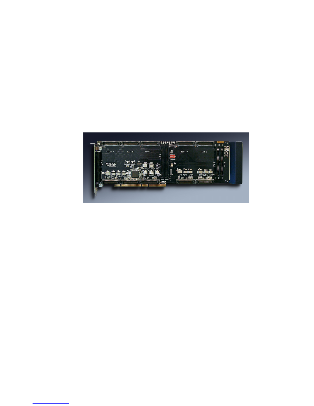
PCI5IP
User Manual
Integrated PCI ó IP Module Carrier
Key Features
Fast Access with integrated PCI ó IP Bridge
5 IP Positions with IO
8/32 MHz IP operation
8/16/32 bit accesses supported
16/32 bit IP module support
Data Alignment – Byte and Word Swapping
Watch Dog Timer
LED’s - Power, IP Access, User
Multi-board support
Manual Revision G1
Corresponding Hardware: Revision G
Fab Number 10-2002-0307
FLASH revision G1

Page 2 of 32 Embedded Solutions
PCI5IP
Dynamic Engineering
150 DuBois St Suite C
Santa Cruz, CA 95060
This document contains information of proprietary interest to Dynamic
Engineering. It has been supplied in confidence and the recipient, by accepting
this material, agrees that the subject matter will not be copied or reproduced, in
whole or in part, nor its contents revealed in any manner or to any person except
to meet the purpose for which it was delivered.
Dynamic Engineering has made every effort to ensure that this manual is
accurate and complete. Still, the company reserves the right to make
improvements or changes in the product described in this document at any time
and without notice. Furthermore, Dynamic Engineering assumes no liability
arising out of the application or use of the device described herein.
The electronic equipment described herein generates, uses, and can radiate
radio frequency energy. Operation of this equipment in a residential area is likely
to cause radio interference, in which case the user, at his own expense, will be
required to take whatever measures may be required to correct the interference.
Dynamic Engineering’s products are not authorized for use as critical
components in life support devices or systems without the express written
approval of the president of Dynamic Engineering.
This product has been designed to operate with IP Modules and compatible userprovided equipment. Connection of incompatible hardware is likely to cause
serious damage.
©2002-2016 by Dynamic Engineering.
Other trademarks and registered trademarks are
owned by their respective manufactures.
Revised July 21, 2016

Page 3 of 32 Embedded Solutions
PRODUCT DESCRIPTION 5!
Theory of Operation 11!
INSTALLATION 12!
ADDRESS MAP 13!
PROGRAMMING 14!
pci5ip_intreg_base 17!
pci5ip_intreg_(a-e) 20!
pci5ip_intreg_int 23!
pci5ip_intreg_dswitch 25!
APPLICATIONS GUIDE 26!
Interfacing 26!
Engineering Kit 26!
IP Module Logic Interface Pin Assignment 27!
Construction and Reliability 28!
MTBF 28!
Thermal Considerations 28!
WARRANTY AND REPAIR 29!
Service Policy 29!
Out of Warranty Repairs 29!
For Service Contact: 29!
SPECIFICATIONS 30!
ORDER INFORMATION 31!
Table of Contents

Page 4 of 32 Embedded Solutions
FIGURE 1! PCI5IP POWER FILTERING 8!
FIGURE 2! PCI5IP RESET CIRCUIT 9!
FIGURE 3! PCI5IP STROBE CONNECTION TABLE 10!
FIGURE 4! PCI5IP ADDRESS MAP 13!
FIGURE 5! PCI5IP CONTROL PORT 17!
FIGURE 6! PCI5IP SLOT CONTROL PORT 20!
FIGURE 7! PCI5IP 16 BIT BYTE SWAPPING 21!
FIGURE 8! PCI5IP 32 BIT BYTE SWAPPING 21!
FIGURE 9! PCI5IP INTERRUPT STATUS PORT 23!
FIGURE 10! PCI5IP USER SWITCH PORT 25!
FIGURE 11! PCI5IP LOGIC INTERFACE 27!
FIGURE 12! PCI5IP LOCATION REFERENCE 32!
FIGURE 13! PCI5IP CONNECTOR REFERENCE 32!
List of Figures

Page 5 of 32 Embedded Solutions
Product Description
IndustryPack® Modules are an important part of solutions for Embedded situations.
Rugged, Small, light .. just right for many applications. IndustryPack® Modules require
a “carrier” to adapt them to the system. Dynamic Engineering has carrier solutions for a
variety of formats. PCI5IP is designed to support PC computer based solutions. Other
supported formats include PCIe, cPCI, PC104p, VPX.
PCI5IP is part of the Dynamic Engineering IP Compatible family of modular I/O
components. PCI5IP provides five IndustryPack® Compatible sites in one PCI slot. Two
of the slot pairs can be used for double wide IP Modules with either 16 or 32 bit IP
Module bus.
PCI5IP is supported with Windows® compliant [WDM32] drivers for XP and 2000
[WFM] for Win7 and Linux [Ubuntu]. VxWorks is in development. The drivers come
with a generic IP driver to allow use with “unknown” IP’s – IP’s that do not have a driver
designed yet. For example, third party IP’s
ID, IO, INT, and MEM access types are supported for read and write cycles. The full 8
Mbytes of address space is allocated to each of the MEM spaces.
The PCI bus is 32 bits wide and most industry packs are 16 bit devices. Byte, word,
and long word accesses are supported. Bytes can be to any address. Word accesses
need to be word aligned. Long word accesses need to be long word aligned. Each of
the access types has a one-to-one correspondence to the hardware. There are no
"extra" accesses with the PCI5IP design.
The Data bus is designed as a 32-bit bus with slots A,C,E on the D15-0 segment. B
and D are on the D31-16 half of the bus. The current hardware compensates and
allows for standard accesses to all slots – software transparent. The BC and DE slots
can be accessed as a 32 bit wide data path. The BC and DE slots are mechanically
aligned for double wide card installation as well as pairs of single wide cards.
A long word access to a 16 bit port will automatically be converted into two back-to-back
IP accesses with the address incrementing between cycles unless the increment
disable function is selected (see Slot control register description). In the increment
disable case the hi or low address can be specified for the double access.
For a read, one 32 bit data word will be returned. For example a long word read to the
ID space would yield $xx50xx49 for many boards as the "0" location has $49 and the
next address has $50. The long word mode happens automatically when all 4 of the
byte lane enables are detected asserted. The overall throughput is greatly enhanced

Page 6 of 32 Embedded Solutions
with this mode of operation. Please note the non-data bytes should be masked, as
many IPs do not drive the “off byte”.
For a long word access to a long word port the 32 bit IP data bus is utilized. Slots B/C
and D/E form 32 bit slots when 32 bit IPs are installed. The access type is automatic
based on the address space used to access the slots. You can use 16 and 32 bit
accesses intermixed without changing your control registers if the IP supports both.
Slot C and E control registers define the access when in 32 bit mode. It may be
necessary to match Slot B clock to slot C and Slot D clock to slot E if your IP uses both.
The address is shifted from long [32] to short [16] by hardware and the byte strobes
used to access the individual bytes or words. If your card has mixed addressing
requirements you may need dual defines to account for the 32 bit and 16 bit addressing.
The PCI bus is defined as little endian and many IPs have their register sets defined to
operate efficiently with a little endian interface. The default settings on the PCI5IP are
“straight through” byte for byte and D15-0 written to address 0x00 before D31-D16
written to address 0x02 when long words are written to 16 bit ports. Please note that
any long word address can be used. The lower data is written to the lower address first,
then the upper data to the upper address. Each slot has a BS and WS control bit to
allow Byte and Word Swapping to be performed to accommodate alternate IP and OS
requirements.
Byte Swapping
16 bit ports
D15-8 ó D7-0
D31-24 óD23-16
32 bit ports
D31-24 => D7-0
D23-16 => D15-8
D15-8 => D23-16
D7-0 => D31-24
Word Swapping will swap D31-16 with D15-0
If byte swapping is enabled and 0x1234 is written to an IP slot, then the IP will see
0x3412. If 0x12345678 is written to a 32-bit port then the IP will see 0x78563412. The
“is written” is defined by the data on the PCI bus. Your software/OS may do its own
conversion before the data gets to the PCI bus.
The byte and word swap controls are separated to allow the conversion to be used for
big-little endian and for register mapping purposes. Each slot has separate controls for

Page 7 of 32 Embedded Solutions
access to that slot.
PCI5IP has a watch-dog timer function which completes the IP access if the IP does not
respond within 7.6 uS. The watch-dog timer has a master status bit and an optional
interrupt output. In addition to the master status each slot control register reports status
for the bus error. Multi-threaded programs can tell if their hardware access caused the
Bus Error even if other threads have accessed other hardware since the bus error was
caused.
The design of PCI5IP tags all accesses from the PCI bus. IP Modules can take longer
than the PCI response specification leading to the use of retry cycles on the PCI bus.
In a single CPU system the retry accesses are done serially. The current IP access will
be the correct one to respond to the retry access. In a multi-CPU system it is possible
to get out of sequence accesses, and potentially have the IP response sent to the
wrong retry access. By storing the PCI parameters for the IP access and only
responding to the correct retry cycle; multiprocessor cross contamination is avoided.
This feature is incorporated beginning with the revision F.
Each slot is programmable for 8 or 32 MHz. operation. The control register has
separate bits for slot A, B, C, D and E. The clocks are locked together and can be
switched at any time. Hardware insures that the clocks switch basis on a clock period
boundary to provide seamless operation.
PCI5IP supports interrupts from each slot with separate mask bits. Two interrupts from
each of the five slots. An interrupt “force” bit is supplied to aide in software
development. The bus error [watch dog timer] can also be an interrupt condition. The
masked interrupts are tied together and connected to INTA on the PCI bus.
PCI5IP has LED's for power, access, and user functions. The supplied voltages are
monitored and an LED illuminated when in tolerance. +12, -12, +5, 3.3. An additional 8
LED's are supplied which are controlled via the control register for user defined
purposes. Five LED’s are controlled by a timer circuit which is activated by the
acknowledge from each of the IP slots.
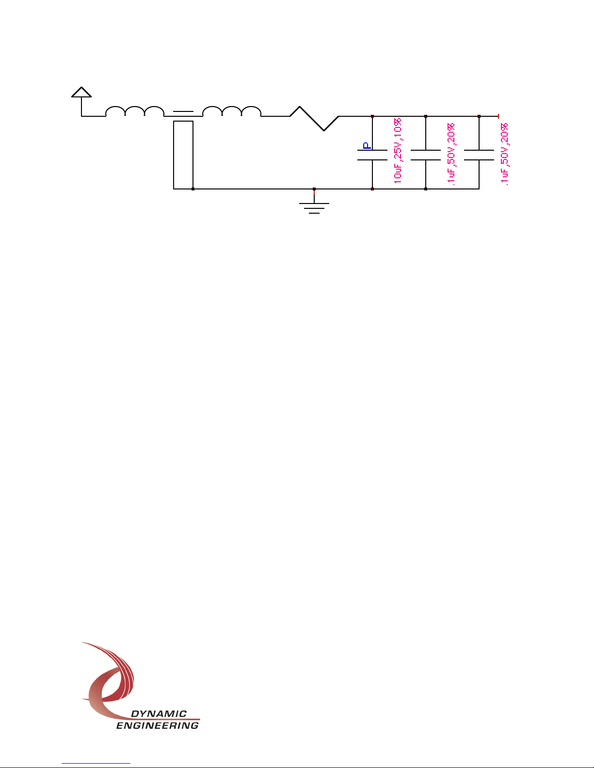
The power to each of the IP slots is individually filtered and fused for +5 and ±12. The
fuses are rated at 2A on the 5V rail and 1.1A on the ±12V rails. PCI5IP is designed to
route maximum power to each slot in parallel. The power supply capabilities for your
chassis may provide additional constraints. Each slot filter has a separate RF filter, bulk
capacitor, “self healing” fuse, and bipass capacitors. A bipass capacitor is located at
each of the power pins on the PCI5IP with the bulk capacitor near the filter pin for
optimum noise rejection, voltage hold-up and local filtering. For power hungry IP’s the
fuses can be replaced with a strap to allow for more than the specified current.
Page 8 of 32 Embedded Solutions
FIGURE 1 PCI5IP POWER FILTERING
With the filter pin on each slot and bulk capacitor each IP is effectively isolated from the
other IP’s mounted to the PCI5IP. Additional work was done in layout to minimize the
amount of cross-slot electronic noise. Each of the IP slots is also isolated from the PCI
interface by the power conditioning. The FPGA uses 3.3 and 2.5V power which is
derived from the 5V supply and bussed on mini-planes to the FPGA. The FPGA is
effectively isolated from the IP slots by the regulators and additional filtering.
PCI5IP is well behaved with low noise power provided to each of the slots. PCI5IP is
designed for analog and digital IP applications including data acquisition,
instrumentation, measurement, command and control, telemetry and other industrial
applications.
An 8 bit "dip switch" is provided on the PCI5IP. The switch configuration is readable via
a register. The switch is for user defined purposes. We envision the switch being used
for software configuration control, PCI board identification or test purposes.
P C I P o w e r
IP Po w e r
F1
L1
Page 9 of 32 Embedded Solutions
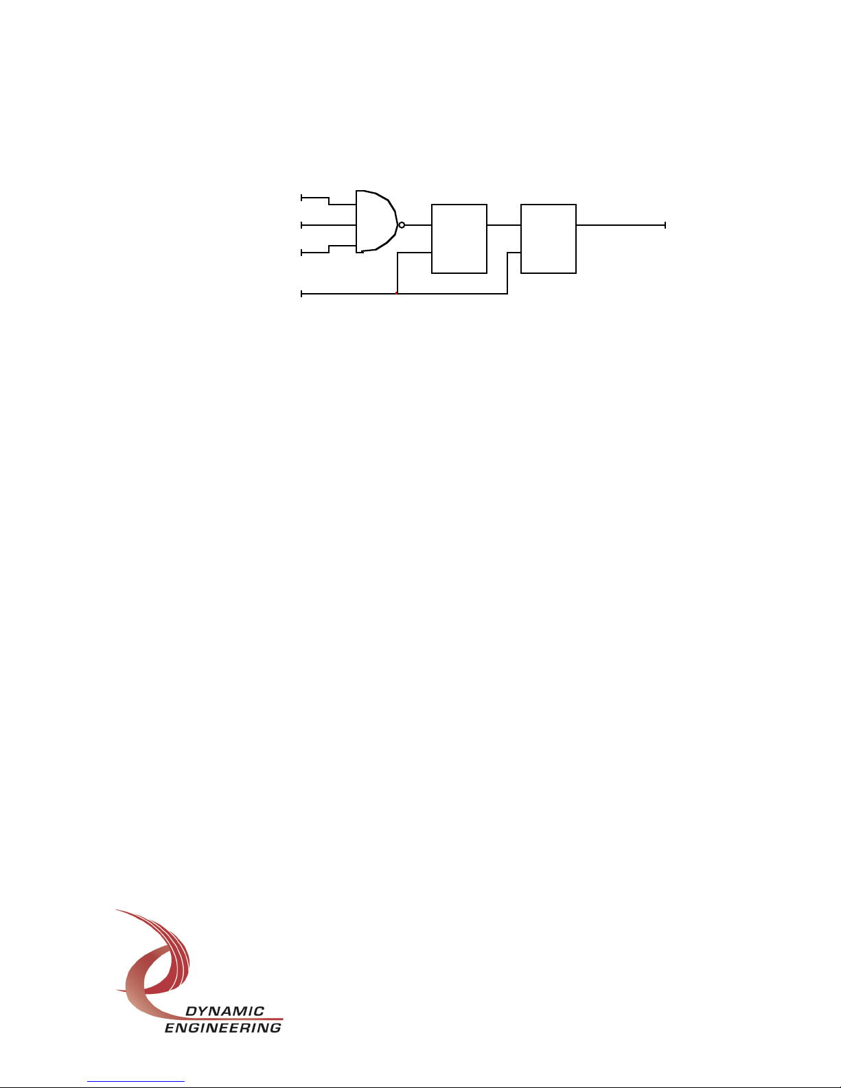
The reset switch provided can be used to reset the IP devices without affecting the PCI
bus. Power, PCI reset, and a control register bit also cause the IP Reset to be
activated. The reset is controlled to be synchronous to the 8 MHz. clock. Alternatively,
the IP-Debug-Bus card can be used for individual slot resets.
FIGURE 2 PCI5IP RESET CIRCUIT
The IO are brought to 50 pin headers. The headers are installed without ejectors to be
PCI compliant [height]. The ejectors can be installed by special request. Routing is
matched length, impedance controlled, and differential on a per IP basis. The
differential pairs are 1-2,3-4,..23-24, 25-50, 26-27… 48-49. With this pattern the
differential pairs can be properly routed for both the IP and Header connectors with
adjacent pin pairs used except for the single 25-50 pair. Frequently 25 and 50 are
grounds. Routing is still 1:1 as well making signal tracing through the carrier easier to
deal with. Dynamic Engineering IP modules take advantage of the differential definition
just outlined.
PCI5IP conforms to the VITA standard for IndustryPack Carriers. This guarantees
compatibility with multiple IndustryPack compatible modules.
PCI5IP conforms to the PCI 2.3 specification and supports both 3.3V and 5V signaling
levels. PCI5IP is accessible in the memory space on the PCI bus. This guarantees
compatibility with other PCI compliant hardware – most PC’s.
The PCI interface is integrated with the IP interface providing superior performance over
designs relying on a separate PCI interface device. In addition to access speed the
higher level of integration results in fewer initialization steps and requirements, more
flexibility in operation, a higher MTBF, and less complex software with only one Base
Address [BAR] to deal with.
If your project can benefit from a "non-standard" implementation, or features that we
have not thought of, or implemented yet please let us know. The Xilinx has room. For
example; if your project will use IP's that can operate at 33 MHz instead of 32, then we
could synchronize the IP and PCI clocks and save several synchronization steps.
C
D Q
C
D Q
IP REFERENCE CLK
IP RESET
VCC DETECT TIMER
RESET REG BIT
PUSH BUTTON

Page 10 of 32 Embedded Solutions
Wired but not yet implemented. (1) All of the DMA control signals are available for a
future revision to implement.
Wired and User implemented. The IP Strobe signal is connected from each IP slot to a
5 pin header to allow for inter-slot user defined communications. The IP specification
does not define what the strobe can be used for. The header is rarely used. If you
need it please add “–STB” to your order number and we will install the 5 pin header for
you. Standard .025” sq. posts suitable for wire-wrap inter-connection.
On each IP Slot the Strobe signal is connected to pin 46.
FLASH memory is used to program the FPGA. Future updates can be added to your
card with the Xilinx Impact tool should you want to make use of a new feature. For
example with the Revision G FLASH, the PCI Core is now a Dynamic Engineering
design. This is important because we have corrected a defect in the core previously
used which interfered with use in external chassis.
FLASH Revisions:
Initial Release A 4/2002, ported from PCI3IP and added 2 positions plus independent
controls
Rev B 6/03 Add independent bus error status bits
Rev C 6/03 Add 32 bit addressing and dual slot operation capability
Rev D 7/03 Add byte and word swap capability
Rev E 6/09 Add protection for multi-processor operation
Rev F 8/09 minor update for 32 bit addressing with multi-processor protection
Rev G 4/16 Update to use DE designed PCI core, add Readable Revision field
Rev G.1 7/16 Update to add Bus Error status bits to base status register and master
bus error clear control. Modification to Bus Error capture logic. Addition
of readable FLASH major and minor revision.
Strobe Pinout on Header
TP1
1 STB A
2 STB B
3 STB C
4 STB D
5 STB E
FIGURE 3 PCI5IP STROBE CONNECTION TABLE

Page 11 of 32 Embedded Solutions
Theory of Operation
PCI5IP is used to bridge from PCI to IP bus specifications. The PCI bus will be the
master in most cases with the IP's being accessed for read or write cycles. The PCI
accesses are handled at the lowest level by the PCI core.
The PCI bus provides multiplexed address and data plus control lines. The data is
separated from the address, and the control lines are decoded to provide the inputs to
the IP Interface state machines. The address is tested to determine which slot the
access belongs to and which type of access to implement. The IP control strobes are
generated. When acknowledge is received the cycle is terminated back to the host.
The PCI bus will see a retry mode while the access is taking place and "disconnect with
data" when the cycle is completed.
Feature List
• PCI Universal Voltage [3.3 or 5V signaling]
• Integrated PCI ó IP conversion for faster access
• 5 IP compatible positions
• Full ID, IO, INT, and Memory space allocated for each IP
• 8 or 32 MHz operation in each slot independently
• byte, word, long word access. 32 bit access to 16 bit slots with static or incrementing
address. 32 bit access to 32 bit slots.
• byte and word swapping for little endian – big endian conversion
• Bus error abort response with slot status
• 1:1 50 pin headers with matched length, impedance controlled differentially routed
traces between IO and header
• IP Reset Switch
• 8 position "DIP Switch" – slot identification when multiple PCI5IP’s are in your system
or for user defined purpose(s)
• 8 User LED’s, 4 Power LED’s, 5 Access LED’s
• Fused Filtered Power with resettable “self healing” fuses in each slot.
• Windows®XP, Win7, Linux Drivers available. Generic IP interface included with driver
to support your IP. Dynamic Engineering driver development available for customized
IP support. [please download the separate Driver manual] VxWorks coming soon.
If you develop a driver for one of our products and are willing to allow others to use it;
we will add it to the web site as a free of charge download and, if desired, give credit to
the author.

Page 12 of 32 Embedded Solutions
Installation
PCI5IP and the IP’s to be mounted should be treated as static sensitive hardware.
The technician should be properly grounded; the mounting and installation process
performed at a static free workstation.
PCI5IP can be installed into any PCI slot with full-length capability. The bezel and PCI
extension bracket securely retain the PCI5IP within the chassis. The PCI5IP with type1
IP Modules installed is PCI legal for height, length and width. Adjacent slots can be
filled with multiple PCI5IP cards.
Ordering options include a right angle connector for position A that protrudes through
the bezel. This is the standard option and helps with cabling. When this option is
ordered a special trimmed rear support is mounted to allow PCI5IP to be rotated
through the chassis rear bezel port while engaging at the rear support. When the –BB
option is ordered a vertical connector is installed, a blank bezel is provided in place of
the cable bezel [designed to allow cables to come through the bezel], and a traditional
offset rear support bracket is provided.
Each of the 5 IP positions can have an IP installed. IndustryPack®s are installed by
pushing the mezzanine card onto the connector pair on the PCI5IP. Each position is
clearly marked. The IO connector is located near the top of the PCI5IP and the IP Bus
connector near the PCI backplane edge. The IP connectors are keyed making
orientation error proof. Please refer to Figure 12 for the position and IO connector
placement.
The IP mounting kit can be utilized to secure the IP to the PCI5IP. Each Dynamic
Engineering IP sold comes with a mounting kit. If you need a replacement or your IP
comes from another manufacturer please order IP-MTG-HW. 1 kit per IP. The kit
includes stainless steel hardware – screws and standoffs.
http://www.dyneng.com/IPHardware.html
If more than one PCI5IP is to be installed into the same system – visible on the PCI bus
the dipswitch can be set to different positions on each card. Software can use the
dipswitch setting to identify which PCI5IP is allocated which address space and
associate specific IP/cables with that PCI5IP so there is positive automatic control of
your system configuration. The Dynamic Engineering Driver makes use of this feature
to allow multiple PCI5IP’s to be used in the same system without identification
challenges.

Page 13 of 32 Embedded Solutions
Address Map
pci5ip_intreg_base 0x00000000 // base control register
pci5ip_intreg_a 0x00001000 // slot A specific clock and interrupt
pci5ip_intreg_b 0x00002000 // slot B
pci5ip_intreg_c 0x00003000 // slot C
pci5ip_intreg_d 0x00004000 // slot D
pci5ip_intreg_e 0x00005000 // Slot E
pci5ip_intreg_dswitch 0x00006000 // User Switch read back port
pci5ip_intreg_int 0x00007000 // Interrupt status read-back
pci5ip_ida_st 0x00110000 // starting address of slot A ID space
pci5ip_idb_st 0x00140000 // starting address of slot B ID space
pci5ip_idc_st 0x00120000 // starting address of slot C ID space
pci5ip_idd_st 0x00150000 // starting address of slot D ID space
pci5ip_ide_st 0x00130000 // starting address of slot E ID space
pci5ip_idbc_st 0x00160000 // starting address of slot B/C ID
pci5ip_idde_st 0x00170000 // starting address of slot D/E ID
pci5ip_ioa_st 0x00210000 // starting address of slot A IO space
pci5ip_iob_st 0x00240000 // starting address of slot B IO space
pci5ip_ioc_st 0x00220000 // starting address of slot C IO space
pci5ip_iod_st 0x00250000 // starting address of slot D IO space
pci5ip_ioe_st 0x00230000 // starting address of slot E IO space
pci5ip_iobc_st 0x00260000 // starting address of slot B/C IO
pci5ip_iode_st 0x00270000 // starting address of slot D/E IO
pci5ip_inta_st 0x00310000 // starting addr of slot A INT space
pci5ip_intb_st 0x00340000 // starting addr of slot B INT space
pci5ip_intc_st 0x00320000 // starting addr of slot C INT space
pci5ip_intd_st 0x00350000 // starting addr of slot D INT space
pci5ip_inte_st 0x00330000 // starting addr of slot E INT space
pci5ip_intbc_st 0x00360000 // starting address of slot B/C INT
pci5ip_intde_st 0x00370000 // starting address of slot D/E INT
pci5ip_mema_st 0x00800000 // starting addr of slot A MEM space
pci5ip_mema_en 0x00FFFFFF // end address of slot A MEM space
pci5ip_memb_st 0x02000000 // starting addr of slot B MEM space
pci5ip_memb_en 0x027FFFFF // end address of slot B MEM space
pci5ip_memc_st 0x01000000 // starting addr of slot C MEM space
pci5ip_memc_en 0x017FFFFF // end address of slot C MEM space
pci5ip_memd_st 0x02800000 // starting addr of slot D MEM space
pci5ip_memd_en 0x02FFFFFF // end address of slot D MEM space
pci5ip_meme_st 0x01800000 // starting addr of slot E MEM space
pci5ip_meme_en 0x01FFFFFF // end address of slot E MEM space
pci5ip_membc_st 0x03000000 // starting address of slot B/C MEM
pci5ip_membc_en 0x037FFFFF // end address of slot B/C MEM
pci5ip_memde_st 0x03800000 // starting address of slot D/E MEM
pci5ip_memde_en 0x03FFFFFF // end address of slot D/E MEM
FIGURE 4 PCI5IP ADDRESS MAP

Page 14 of 32 Embedded Solutions
The address map provided is for the local decoding performed within PCI5IP.
The addresses are all offsets from a base address. The host the PCI5IP is
installed into provides the base address and interrupt level. Your software will
need to concatenate the base address + PCI5IP address + IP Local address to
create a pointer to each programmable feature on your IP.
Programming
The address map will connect to the IP module. The IP board description will
provide the local addresses. If you are in a Windows or Linux environment you
can use a Dynamic Engineering Driver for the carrier and potentially the IP.
Complete information is provided within this manual to allow customers who use
another OS or want to write their own interface to do so.
Dynamic Engineering can write a driver for your IP to interface with our carrier(s)
even if it is not “one of ours”. Please contact engineering@dyneng.com with your
requirements if you are interested in this service.
The host system will search the PCI bus to find the assets installed during poweron initialization. The VendorId = 0x10EE and the CardId = 0x000B for the
PCI5IP. Interrupts are requested by the configuration space. The VendorId and
CardId parameters are used by the OS to identify the card and in some cases
launch the plug and play installation process. The interrupt level expected and
style is also set in the registry.
Once the initialization process has occurred and the system has assigned an
address range to the PCI5IP card, the software will need to determine what the
address space is. We refer to this address as base0 in our software.
The next step is to initialize the PCI5IP. The default of no interrupts enabled and
8 MHz. operation will be valid in many cases. The base register for the PCI5IP
and specific slot registers A-E can be initialized to change the default parameters
to suite your requirements. Please refer to the register map definitions for more
information.
Access to your installed IP is done by accessing base0 + slot address + IP offset.
The slot address is defined in the memory map. For example to read your IP in
slot D IO space: *(base0 + pci5ip_iod + ip offset) = data. Each slot and memory
type [IO, ID, INT, Mem] has a unique address space for 20 defined address
spaces [non-32 bit] plus the PCI5IP internal address space. The internal
registers are defined in the following pages.

Page 15 of 32 Embedded Solutions
Please note the Dynamic Engineering Windows® and Linux drivers for PCI5IP
take care of communicating with the system, discovering the address ranges and
interrupt levels and supporting the IP Module level drivers. The SW is included
with your purchase of PCI5IP. Additional HW support tools are available in the
form of an engineering kit.
Dynamic Engineering IP Module drivers are automatically launched as the
Carrier level driver detects the IP Module during initialization. Multiple Modules
of the same type and mixed modules are supported. Third party modules are
supported with a Generic Driver included with the carrier level driver. IP Module
drivers can work with any of the Dynamic Engineering IP Module Carriers for
PCI.
The IP Module Driver communicates with the Carrier level driver to discover the
carrier it is mounted to and the slot. With the carrier and slot information
deterministic control of hardware is possible in a PCI system along with flexibility.
The Carrier DIPSWITCH is used to differentiate one from another in a multiple
carrier system, and the slot number is used to further differentiate between
multiple cards of the same type.
The IP module positions are labeled A-E in the silk for identification.
PCI5IP has an integrated PCI interface with IP bridge. The integrated approach
simplifies programming with only one base address and fewer parameters to
have to initialize. The integrated approach is also a faster access approach
leading to higher performance in your system.
Higher performance for your system can be achieved by matching the IP register
model to the OS and user software model that you are using, selecting the
optimal IP reference clock rate and access types.
PCI5IP has individual clock selection for each of the IP modules. Access time is
reduced when the IP clock rate is set to 32 MHz. PCI5IP can handle any mixture
of clock requirements. Make sure that the IP can handle the higher rate. All
Dynamic Engineering IP Modules are rated for both 8 and 32 MHz operation.
PCI5IP can handle byte, word and long word accesses from the PCI bus. The
state machine within the bridge will automatically select 16 or 32 bit IP width
based on the address space utilized. 32 bit accesses to 16 bit ports will be
converted to double accesses. 32 bit accesses to 32 bit ports will be handled in
a single access. The Byte Swap [BS], Word Swap [WS], Address Increment, and

Page 16 of 32 Embedded Solutions
Word High allow the accesses to be customized for the IP installed for optimum
performance. 32 bit accesses to 16 bit ports are faster than individual 16 bit
accesses and frequently easier to write software for. For example if your IP has
a 24 bit port with 16 bits in one register and 8 in the next you can write all 24
with one 32 bit access. With word and byte swapping you can account for the
organization of the registers on the IP. Some IP’s convert 16 bit accesses to
double 8 bit accesses – IP-QuadUART for example. If your IP has 16:8
conversion then you can write 32 bits and get 4 – 8 bit writes to your IP in one
access.
Read the IP manual and see what strategy is best to communicate with that card
then adapt the settings on the PCI5IP to optimize your accesses to that IP. With
separate control registers for each installed IP you can run different strategies for
each installed IP as appropriate.

Page 17 of 32 Embedded Solutions
Register Definitions
pci5ip_intreg_base
[$00 Main Control Register Port read/write]
CONTROL REGISTER 0
DATA BIT DESCRIPTION
31 Reset 1 = reset IPs 0 = normal
30-14 spare
13 INT FORCE 1 = FORCE 0 = NORMAL
12 Master INT EN 1 = ENABLED 0 = DISABLED
11 spare
10 Bus Error Status Master Clear
9 Bus Error Int/Status Clear
8 Bus Error Int En
7 LED7 1 = ON 0 = OFF
6 LED6
5 LED5
4 LED4
3 LED3
2 LED2
1 LED1
0 LED0
FIGURE 5 PCI5IP CONTROL PORT
Reset when set causes a reset to the IP slots. Reset is active as long as the
Reset signal is asserted. Reset is synchronized to the IP clock per the IP
interface specification. The duration is controlled by the user software. 200 mS
is a suggested minimum time to enable for resetting purposes. In addition there
is a device on board which causes an IP reset of 200+ mS when a power
transition to the powered on state is detected.
LED7-0 are the user LED's situated at the right side of the card near Slot E.
Each LED can be activated by setting the corresponding data bit and deactivated
by clearing the same bit. The LED’s are aligned: 0x12 would be
off off off on off off on off [7ó0]
Spare means undefined, and is suggested to be written as ‘0’ to allow for
commonality with future enhancements.
INT FORCE will, when set, cause INTA on the PCI bus to be asserted. This bit

Page 18 of 32 Embedded Solutions
can be useful for software debugging. Set this to simulate an IP interrupt when
the hardware is not available. The master interrupt must be enabled to have an
effect.
Master Interrupt Enable must be set to allow the IP or other interrupt conditions
to become an interrupt on the PCI bus. 1 = enabled. 0 = disabled or masked.
Bus Error Int En when ‘1’ allows the bus error detection circuit to cause an
interrupt to the host when a Bus Error is detected. The status is available on the
Interrupt status register. When ‘0’ the status is still valid but no interrupt is
generated when a bus error is detected. The bus error is detected when an
access to one of the IP slots is not responded to by IP hardware within the timeout period of approximately 7.3 uS.
The bus error circuit is always enabled and automatically responds as if the IP
had responded. The data read will typically be $FF if the IP is not driving the bus
for a bus error read. For a bus error during a write, the write should be assumed
to not have taken place. The host will not know that the bus error has taken
place unless the host checks the status. The interrupt can provide a prompt to
check the status during operation. During initialization if the software is checking
to “see” what is installed or what address range is valid on an IP, the status can
be polled to see if the IP responded.
The Bus Error State-machine has 3 states, Idle, Armed, Clear. When in Idle
[default reset condition] the SM is waiting for a Bus Error to occur. The trigger is
the logical OR of any of the 7 bus error status bits from the 5 IP positions
including the two for 32 bit wide cards. When detected the SM moves to the
Armed state setting the status bit. The status bit is masked to become the
interrupt request if enabled. When SW sets the INT Clear bit the SM moves to
the CLEAR state and waits for the slot status to also be cleared before returning
to IDLE. This is to prevent the cleared SM from retriggering before the slot status
is cleared.
Bus Error Status / INT Clear when ‘1’ will clear the Bus Error status bit and
interrupt request [if enabled]. The Clear bit needs to be reset to ‘0’ to be able to
capture the next Bus Error as well as the slot status bit(s). The bus error timer
hardware operates independent of clearing the status and will continue to
monitor and intercede whether the status is read or cleared.
Each of the slot registers has an additional status bit to identify which slot caused
the bus error. The slot register bus error status is repeated in the upper bits to

Page 19 of 32 Embedded Solutions
allow single read ISR operation. Please see the PCI5IP Interrupt Register
description.
Bus Error Status Master Clear when set ‘1’ causes the Bus Error Status bits in all
of the channels to be cleared as well as the state-machine that manages the bus
error interrupt. Remember to reset to ‘0’ for normal operation. Usually only
needed after enumeration / slot discovery. The unfilled locations will have bus
error status set which needs to be cleared for proper operation of the bus error
interrupt state machine.

Page 20 of 32 Embedded Solutions
pci5ip_intreg_(a-e)
[$01000,2000,3000,4000,5000 Slot Control Register Port read/write]
Slot CONTROL REGISTER (A-E)
DATA BIT DESCRIPTION
31-9 Undefined
8 bus error status/clear
7 word swap control
6 byte swap control
5 Interrupt Enable 1
4 Interrupt Enable 0
3 High Word Access
2 Increment Disable
1 spare
0 Speed Control 1 = 32 MHz, 0 = 8 Mhz
FIGURE 6 PCI5IP SLOT CONTROL PORT
Speed Control selects the slot clock speed. 1 = 32 MHz. 0 = 8 MHz. Clock
selection change can be made at any time. Each slot has a separate speed
control bit. Default is 8 MHz.
Increment Disable, when ‘1’, turns off the address increment that normally
occurs between 16-bit IP cycles when a 32-bit PCI access is performed. This is
useful if, for instance, a FIFO is mapped to a single IP address since it allows
double IP accesses to the same address with a single PCI transfer. All types of
access are affected (i.e. MEM, IO, INT, and ID). Each slot has independent
controls and operation. Only 32 bit accesses are affected.
High Word Access controls which 16-bit word is accessed when the Increment
Disable is asserted. When ‘0’ the lower word is accessed twice, when ‘1’ the
upper word is accessed twice. This bit only has an effect when the Increment
Disable bit is ‘1’. For correct functioning, please make sure the PCI access is on
a long-word boundary.
Interrupt Enable 0,1 individual masks for the 2 interrupts from each of the 5
slots. 0 corresponds to INT0 and 1 corresponds to INT1.
Byte Swap when ‘1’ causes the byte lanes to be swapped. For a 16-bit access
the upper byte is swapped with the lower byte. For a 32-bit access to a 16-bit
port the upper and lower of each word are swapped. For a 32-bit access to a 32-
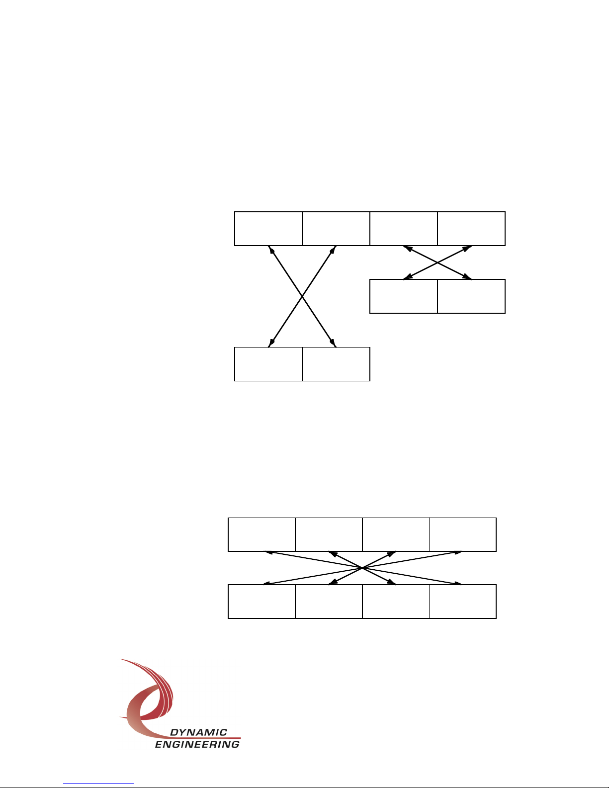
Page 21 of 32 Embedded Solutions
bit port the bytes and words are swapped so D31-24 becomes D7-0 etc. Byte
Swap when ‘0’ provides the data on the same byte lanes that the PCI bus
provides them on. Byte Swapping can be used in conjunction with the Word
Swap feature for big endian ó little endian conversion.
16 bit ports
D15-8 ó D7-0
D31-24 óD23-16
FIGURE 7 PCI5IP 16 BIT BYTE SWAPPING
32 bit ports
D31-24 ó D7-0
D23-16 ó D15-8
D15-8 ó D23-16
D7-0 ó D31-24
FIGURE 8 PCI5IP 32 BIT BYTE SWAPPING
Byte 3 Byte 2 Byte 1 Byte 0
PCI Data
D31 D0
Byte 2 Byte 3
D0D31
Byte 0 Byte 1
IP Bus Access
Byte 3 Byte 2 Byte 1 Byte 0
PCI Data
D31 D0
Byte 0 Byte 1
D0D15
IP Bus
First Access
Byte 0 Byte 1
IP Bus
Second Access
D0D15

Page 22 of 32 Embedded Solutions
Word Swap when ‘1’ will cause the upper and lower words to be swapped. Data
written to PCI D15-0 will be driven onto the IP bus as if it originated on D31-16.
Word Swap when ‘0’ leaves the data on the PCI word definitions. Please note
that Word Swap has no effect on 32 bit accesses to 32 bit IP Module ports.
The IP bus interface state-machine will move data from D15-0 to the “0” address
and from PCI D31-16 to the IP “2” address. IP addresses are word based for
non-32 bit capable accesses [even with 32 bit transfers]. The PCI bus will write
data to either the upper or lower words and apply the corresponding CBE byte
lane strobes. The PCI5IP hardware will translate the data to D15-0 on the IP.
Word swapping can be used effectively for big endian ó little endian translation
and to accommodate IPs with registers that can be more effectively accessed in
reverse order. For example: if the IP registers are organized with the MS data at
address 0x00 and the LS data at 0x02 then a single 32 bit write can be made to
0x00 with address incrementing enabled and word swapping enabled so that the
PCI D31-16 data is written to IP 0x00 and the PCI D15-0 data is written to IP
0x02. If the IP registers have data 16 bits or less then word swapping will not be
needed.
With the combination of Byte and Word Swapping plus address definition any
byte/word can be direct to/from any destination. Big ó little endian issues can
be resolved and IP architecture optimized for software access.
The bus error bit is a status bit with a write clear. The clear is active at the time
of the write only and does not need to be reset. If the bus error bit is set when
the register is read then a bus error has occurred on this slot. Once set the bit
will remain set until explicitly cleared by writing a ‘1’ to this bit position. This bit
must be cleared to re-arm the Bus Error Interrupt / Master status capability.

Page 23 of 32 Embedded Solutions
pci5ip_intreg_int
[$7000 PCI5IP interrupt register read only]
CONTROL REGISTER 0
DATA BIT DESCRIPTION
31 ‘0’
30 Bus Error Slot DE
29 Bus Error Slot BC
28 Bus Error Slot E
27 Bus Error Slot D
26 Bus Error Slot C
25 Bus Error Slot B
24 Bus Error Slot A
23 ‘0’
22 Bus Error 1= occurred 0 = none
21 UNMASKED E1
20 UNMASKED E0
19 UNMASKED D1
18 UNMASKED D0
17 UNMASKED C1
16 UNMASKED C0
15 UNMASKED B1
14 UNMASKED B0
13 UNMASKED A1
12 UNMASKED A0 1 = SET 0 = NOT SET
11 ‘0’
10 INTRN 1 = SET, 0 = NOT SET
9 MASKED E1
8 MASKED E0
7 MASKED D1
6 MASKED D0
5 MASKED C1
4 MASKED C0
3 MASKED B1
2 MASKED B0
1 MASKED A1
0 MASKED A0 1 = SET 0 = NOT SET
FIGURE 9 PCI5IP INTERRUPT STATUS PORT
Interrupt requests from each of the IP slots are available as status from this port.
The interrupt requests are inverted to make them active high for software
usability. The requests are available in a masked and unmasked form to allow
polling with the PCI interrupt masked off. When an interrupt is detected this
register should be read to determine the source or sources and appropriate
action taken to clear the interrupt at the IP or clear the mask on PCI5IP.

Page 24 of 32 Embedded Solutions
PCI5IP provides direct access to the interrupt space. If the IP causing the
interrupt requires an interrupt vector fetch to clear the interrupt the appropriate
INT space should be accessed. Address bit A1 selects between Int0 and Int1.
A1 follows the word address to allow access to both INT0 and INT1 clearing
addresses within the INT space.
Most IP’s support having an interrupt vector. The vector associated with INT0
can be accessed from base0 + pci5ip_int[slot]_st + 0x00. The vector associated
with INT1 can be accessed from base0 + pci5ip_int[slot]_st + 0x02. If the IP
does not require a Vector fetch to clear the interrupt then proceed with IO or
other accesses as necessary.
The Bus Error status bit is set high when a Bus Error is handled by the internal
watch dog timer circuit. The status will stay high until cleared with the Bus Error
Int / Status Clear bit in the base control register. The Bus Error status bit is or’d
into the interrupt request logic and if enabled will cause a level sensitive interrupt
to the host. The interrupt will remain asserted until the status is cleared. In
addition the slot bus error status bits are available to determine which position(s)
have caused Bus Errors.
Please see the Base Control register for the definitions of the enable and clear
control bits.

Page 25 of 32 Embedded Solutions
pci5ip_intreg_dswitch
[$6000 User Switch Port read only]
DipSwitch Port
DATA BIT DESCRIPTION
23-16 Revision Minor
15-8 Revision Major
7-0 Sw7-0
FIGURE 10 PCI5IP USER SWITCH PORT
The user switch is read through this port. The bits are read as the lowest byte.
Access the port as a long word and mask off the undefined bits. Read only. The
dip-switch positions are defined in the silkscreen. For example the switch figure
below indicates a 0x12.
The switch can be used for any user purpose or to identify a particular PCI5IP in
a system with more than one card installed. Dynamic Engineering Driver
software uses the switch for slot identification.
The FLASH revision is read from this port. The Revision Major field is also
mapped to the PCI interface and reported through the configuration space. This
field can be read and used as a switch when new features are added to the card.
The Minor revision is rolled whenever changes are made no matter how small
[and released]. The Major field is updated when larger changes are made.
1
7 0
0

Page 26 of 32 Embedded Solutions
Applications Guide
Interfacing
Some general interfacing guidelines are presented below. Do not hesitate to
contact the factory if you need more assistance.
Start-up
Make sure that the "system" can see your hardware before trying to access it.
Many BIOS will display the PCI devices found at boot up on a "splash screen"
with the VendorID 0x10EE and CardId 0x000B and an interrupt level. Look
quickly! If the information is not available from the BIOS then a third party PCI
device cataloging tool will be helpful. We use PCIView.
Watch the system grounds. All electrically connected equipment should have a
fail-safe common ground that is large enough to handle all current loads without
affecting noise immunity. Power supplies and power consuming loads should all
have their own ground wires back to a common point.
Power all system power supplies from one switch. Connecting external
voltages to the PCI5IP when it is not powered can damage it, as well as the rest
of the host system. This problem may be avoided by turning all power supplies
on and off at the same time. This applies more to the IP's installed onto the
PCI5IP than the PCI5IP itself, and it is smart system design when it can be
achieved.
Connector definition. Slot A's IO connector is tied 1:1 to I/O A which is nearest
the card edge on the Slot A side. Slot B is tied to I/O B and Slot C to I/O C, Slot
D to I/O D and Slot E to I/O E. The IO connectors are standard 50 pin ribbon and
discrete wire compatible. Please refer to the diagram near the end of the
manual. The interconnection traces are differentially routed, impedance
controlled, and matched length for each slot separately.
Engineering Kit
PCI5IP is tested in a Windows® environment. Please consider purchasing the
engineering kit for the PCI5IP. When the driver option is selected the
engineering kit includes our test suite as reference code. The reference SW is
supplied as source.

Page 27 of 32 Embedded Solutions
IP Module Logic Interface Pin Assignment
The figure below gives the pin assignments for the IP Module Logic Interface on
the PCI5IP slots A,C,E. Slots B, D have the upper half of the data bus in place of
D15-0 and the upper strobes BS3,2 in place of BS1,0. Also see the User Manual
for your IP board(s) for more information.
GND GND 1 26
CLK +5V 2 27
Reset* R/W* 3 28
D0 IDSEL* 4 29
D1 DMA-reserved 5 30
D2 MEMSEL* 6 31
D3 DMA-reserved 7 32
D4 INTSEL* 8 33
D5 DMA-reserved 9 34
D6 IOSEL* 10 35
D7 reserved 11 36
D8 A1 12 37
D9 DMA-reserved 13 38
D10 A2 14 39
D11 n/c 15 40
D12 A3 16 41
D13 INTREG0* 17 42
D14 A4 18 43
D15 INTREQ1* 19 44
BS0* A5 20 45
BS1* Strobe 21 46
–12V A6 22 47
+12V Ack* 23 48
+5V reserved 24 49
GND GND 25 50
NOTE 1: The error signals is defined by the IP Module Logic Interface Specification, but not used by this
Carrier. See the Specification for more information.
NOTE 2: The layout of the pin numbers in this table corresponds to the physical placement of pins on the
IP connector. Thus this table may be used to easily locate the physical pin corresponding to a desired
signal. Pin 1 is marked on the carrier. Please note that the PCI5IP revision 2 and later use SMT
connectors. Older PCI5IP boards have a slightly different mechanical configuration for the connectors.
FIGURE 11 PCI5IP LOGIC INTERFACE

Page 28 of 32 Embedded Solutions
Construction and Reliability
IP Modules were conceived and engineered for rugged industrial environments.
The PCI5IP is constructed out of 0.062 inch thick high temperature ROHS
compliant FR4 material.
Through hole and surface mounting of components are used. High insertion and
removal forces are required, which assists in the retention of components.
The IP Module connectors are keyed and shrouded with Gold plated pins on both
plugs and receptacles. They are rated at 1 Amps per pin, 200 insertion cycles
minimum. These connectors make consistent, correct insertion easy and reliable.
The IP Module can be secured against the carrier with the connectors. If more
security against vibration is required then IP mounting kit can be used to attach
the IP to the carrier. Dynamic Engineering has mounting kits available if your IP
did not come with one. http://www.dyneng.com/IPHardware.html
MTBF
PCI5P has been modeled with Belcore reliability prediction software. The MTBF
is reported as 1,099,222 Hrs. GB 25C.
Thermal Considerations
PCI5IP design consists of CMOS circuits. The power dissipation due to internal
circuitry is very low. The installed IP Modules may require forced air cooling. With
the one degree differential temperature to the solder side of the board external
cooling is easily accomplished.

Page 29 of 32 Embedded Solutions
Warranty and Repair
Please refer to the warranty page on our website for the current warranty offered
and options.
http://www.dyneng.com/warranty.html
Service Policy
Before returning a product for repair, verify as well as possible that the suspected
unit is at fault. Then call the Customer Service Department for a RETURN
MATERIAL AUTHORIZATION (RMA) number. Carefully package the unit, in the
original shipping carton if this is available, and ship prepaid and insured with the
RMA number clearly written on the outside of the package. Include a return
address and the telephone number of a technical contact. For out-of-warranty
repairs, a purchase order for repair charges must accompany the return.
Dynamic Engineering will not be responsible for damages due to improper
packaging of returned items. For service on Dynamic Engineering Products not
purchased directly from Dynamic Engineering contact your reseller. Products
returned to Dynamic Engineering for repair by other than the original customer
will be treated as out-of-warranty.
Out of Warranty Repairs
Out of warranty repairs will be billed on a material and labor basis. Customer
approval will be obtained before repairing any item if the repair charges will
exceed one half of the quantity one list price for that unit. Return transportation
and insurance will be billed as part of the repair and is in addition to the minimum
charge.
For Service Contact:
Customer Service Department
Dynamic Engineering
150 DuBois St. Suite C
Santa Cruz, CA 95060
831-457-8891
831-457-4793 fax
support@dyneng.com

Page 30 of 32 Embedded Solutions
Specifications
Logic Interfaces: IP Logic Interface, PCI Interface -33 MHz. 32 bit, universal signaling
Access types: IO, ID, MEM, INT IP Spaces supported via PCI bus accesses
CLK rates supported: 8 MHz or 32 MHz slot by slot selectable. 33 MHz. PCI
Software Interface: Control Registers, and Installed IP. Programming procedure
documented in this manual
Access Modes: LW, Word or Byte to IP registers LW can be converted to two word
accesses or as a LW to a 32 bit IP. LW to Internal PCI Interface Control
registers. Bus error detection and handling.
Access Time: Typical access time with 32 MHz. IP and double access mode is 500 nS.
Interrupt: 2 per IP slot with separate enables., Programmable Bus error interrupt
DMA: No DMA Support implemented at this time
Onboard Options: All Options are Software Programmable
Interface: 50 pin Header Connectors with differentially routed, controlled
impedance, matched length per connector. Option for ejectors.
Dimensions: Full length PCI board. With front bezel and rear mounting bracket.
Construction: High Temp ROHS compliant FR4 Multi-Layer Printed Circuit, Through
Hole and Surface Mount Components.
Power: RF filtered and fused to each IP slot. Resettable “self healing”
fuses.
User 8 position software readable switch
8 software controllable LED's
Other LED LED's (4) monitored power (±12,5, 3.3) LED’s (5) used to show
IP acknowledge to access – 1 per position.
Slots 5 single wide IP slots with double wide and 32 bit capability in
slot pairs B/C and D/E
Temperature Range -40Có+85C Components Standard
Temperature Coefficient: 2.17 W/oC for uniform heat across Carrier
MTBF 1,099,222 Hrs. GB 25C

Page 31 of 32 Embedded Solutions
Order Information
Standard temperature range -40ó85øC
PCI5IP http://www.dyneng.com/pci5ip.html
Full length PCI card with 5 IP positions
-STB Add Strobe Header
-CC Add conformal coating
-ROHS Add ROHS processing and label.
-EJ Add latch block release/retention mechanism
to ribbon cable connectors. Please note this
option is slightly out of spec for PCI height.
-BB Switch to blank bezel. Standard is cable
egress friendly with cutout. Changes position
A IO connector from right angle through the
bezel to vertical.
IP-DEBUG-BUS http://www.dyneng.com/ipdbgbus.html
IP test points, reset switch, fused power, quick
switch isolated interface lines to allow hot
swapping of IP cards.
IP-DEBUG-IO http://www.dyneng.com/ipdbgio.html
Isolate the IO connector to help with
debugging. 50-pin header for system cable
connection. 50 testpoints suitable for wirewrap to allow loop-back connections.
HDRterm50 http://www.dyneng.com/HDRterm50.html
50-pin header to 50 screw terminal converter
with DIN rail mounting.
HDRcabl50 50 pin ribbon cable compatible with PCI5IP
and HDRterm50. Various lengths off-the-shelf,
and custom
All information provided is Copyright Dynamic Engineering

Page 32 of 32 Embedded Solutions
FIGURE 12 PCI5IP LOCATION REFERENCE
FIGURE 13 PCI5IP CONNECTOR REFERENCE
50 Pin Header
Pin 1
Pin 2
Pin 50 Pin 49
The PCI5IP has 5 slots (A,B,C,D,E) and 5 header
connectors associated with those slots.
The wiring is 1:1 from the IP IO connector to the PCI5IP
header connector. The connectors are numbered to
match standard ribbon cable as shown in the figure to
the right.
Matched length impedance controlled traces are used
between the IO connector and Header connector.
IO Connector A is right angle standard and can
optionally be populated with a vertical header.
USER
SWITCH
7<----0
Reset
Switch
A B C
A
B C
D E
D E
Power & Access
LEDS
User LEDs
 Loading...