

DX Radio Systems 9000V5 Service Manual
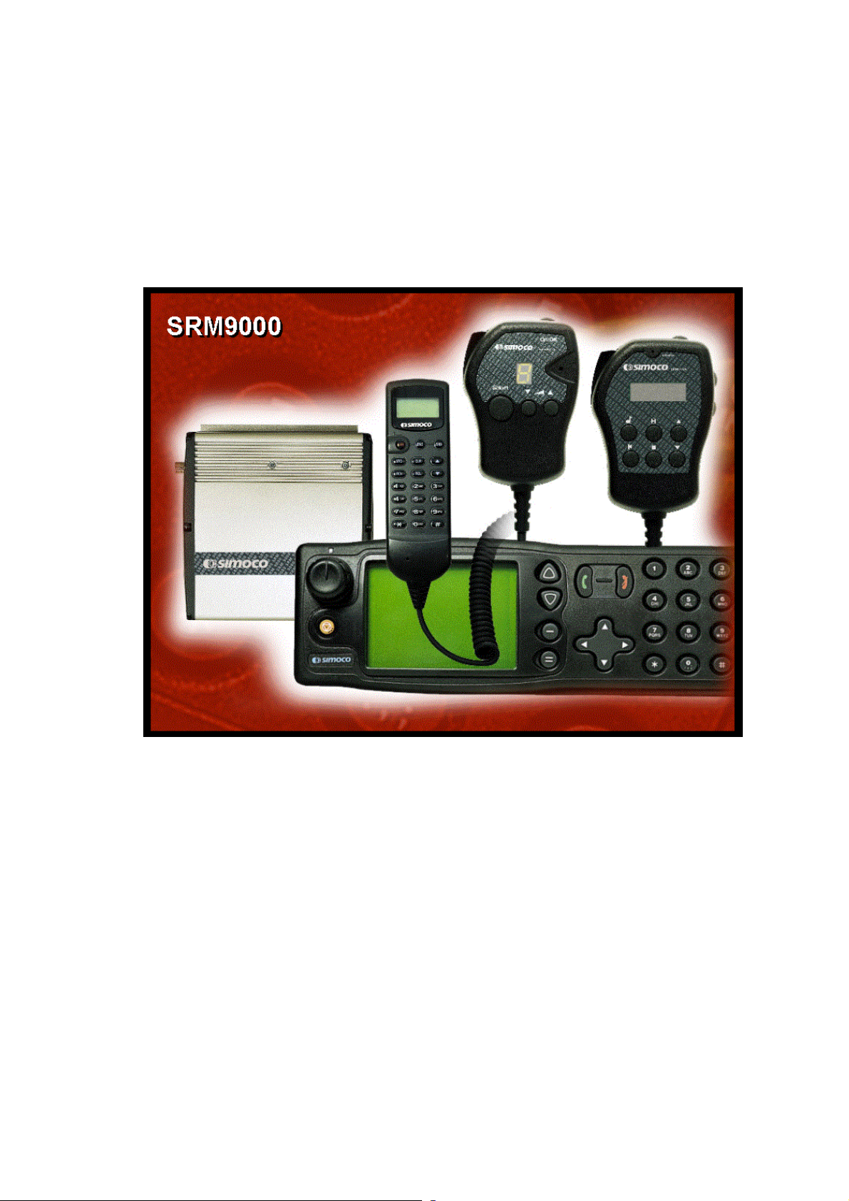
SRM 9000 Series
FM VHF/UHF Mobile Radio Transceiver
SERVICE MANUAL
TNM-M-E-0001
October 2000
Draft D
abcde
DRAFT D
Revision History
Revision Editor Date Revision Details
1.0 J. McB 30/03/2000 Initial Release
Draft A A.G. June 2000 Partial re-format to Simoco Europe standard.
Draft B P.N. 04/07/2000 Rev6 Schematics, UW Band & Appendix
updates
Draft C P.N. 31/07/2000 Still in progress – not to be released!
Updated with E0,AC,TK,UW rev7 schematics &
layouts
Revised Block Diagram.
9010 mic, corrected alignment instructions
Draft C5 A.G. 17-07-2000 Update to Draft C from Simoco Pacific.
Draft D A.G. 27-09-2000 Amended text: Variants; Tech Spec & App B.
List of Associated Publications
Document No. Description Issued By
TNM-I-E-0005 SRM9000 Series Installation Instructions Simoco Europe
TNM-U-M-0001 SRM9010 PMR/Trunk Operating Instructions Simoco Europe
TNM-U-E-0013 SRM9020 PMR Operating Instructions Simoco Europe
TNM-U-E-0014 SRM9025 PMR Operating Instructions Simoco Europe
TNM-U-E-0015 SRM9025 Trunk Operating Instructions Simoco Europe
TNM-U-E-0003 SRM9030 PMR Operating Instructions Simoco Europe
TNM-U-E-0004 SRM9030 Trunk Operating Instructions Simoco Europe
TNM-M-E-0001 Page ii

DRAFT D
Table of Contents
1. INTRODUCTION............................................................................................................1
1.1 GENERAL........................................................................................................................1
1.2 SCOPE ...........................................................................................................................1
1.3 DESCRIPTION..................................................................................................................1
1.4 PRODUCT VARIANTS AND FACILITIES ...............................................................................2
1.5 GLOSSARY......................................................................................................................5
2. SERVICE PHILOSOPHY ...............................................................................................6
2.1 SERVICE CONCEPT .........................................................................................................6
2.2 WARRANTY.....................................................................................................................6
2.2.1 Service within and out of warranty........................................................................6
2.2.2 Ancillary Items.......................................................................................................6
2.3 SOFTWARE POLICY.........................................................................................................6
2.4 ADJUSTMENT AND ALIGNMENT.........................................................................................7
2.5 TECHNICAL SPECIFICATION..............................................................................................8
2.5.1 General .................................................................................................................8
2.5.2 Transmitter............................................................................................................9
2.5.3 Receiver..............................................................................................................10
2.5.4 Signalling.............................................................................................................11
2.5.5 Environmental.....................................................................................................12
3. TECHNICAL DESCRIPTION .......................................................................................13
3.1 RECEIVER.....................................................................................................................13
3.1.1 Front End Filters and RF Amplifier......................................................................13
3.1.2 First Mixer and IF Section...................................................................................13
3.1.3 Quadrature Demodulator....................................................................................15
3.1.4 Receiver Audio Processing.................................................................................15
3.2 TRANSMITTER...............................................................................................................15
3.2.1 Drivers and PA Stages........................................................................................15
3.2.2 Power Control .....................................................................................................17
3.2.3 Antenna Changeover and Harmonic Filter..........................................................17
3.2.4 Transmitter Audio Processing.............................................................................17
3.3 FREQUENCY SYNTHESISER............................................................................................19
3.3.1 General ...............................................................................................................19
3.3.2 PLL......................................................................................................................19
3.3.3 VCO ....................................................................................................................19
3.3.4 Negative Bias Generator and Loop Filter............................................................19
3.3.5 Phase Modulator.................................................................................................19
3.3.6 Reference Oscillator ...........................................................................................20
3.4 CONTROL .....................................................................................................................20
3.4.1 DSP and FPGA...................................................................................................20
3.4.2 DSP Clock Oscillator...........................................................................................22
3.5 MEMORY ......................................................................................................................22
3.5.1 Multiplexer...........................................................................................................22
3.6 POWER SUPPLIES.........................................................................................................22
3.6.1 Power On Function .............................................................................................22
3.6.2 Power Supplies...................................................................................................23
4. ALIGNMENT ................................................................................................................25
4.1 TEST EQUIPMENT ....................................................................................................25
4.2 TEST SET UP .................................................................................................................27
4.2.1 COMMS Set up...................................................................................................28
4.2.2 Radio Preparation...............................................................................................29
TNM-M-E-0001 Page iii

DRAFT D
4.2.3 ALIGNMENT PROCEDURE...............................................................................30
5. REPLACEABLE PARTS..............................................................................................39
6. CIRCUIT DIAGRAMS AND PARTS LIST....................................................................41
6.1 LIST OF ILLUSTRATIONS.................................................................................................41
List of Figures
Figure 3-1 VHF/UHF Receiver Block Diagram .......................................................................14
Figure 3-2 VHF/UHF Transmitter Block Diagram ...................................................................16
Figure 3-3 VHF/UHF Synthesiser, Block Diagram.................................................................. 18
Figure 3-4 VHF/UHF Control Block Diagram .......................................................................... 21
Figure 4-1 SRM9000 Programming & Alignment Breakout Box ............................................. 26
Figure 4-2 SRM9000 Speaker Output Breakout Box..............................................................26
Figure 4-3 Test Set up ............................................................................................................ 27
Figure 5-1 Replaceable Parts ................................................................................................. 39
Figure 5-2 Band-Specific Parts ...............................................................................................40
Figure 6-1 SRM9000 Block Diagram ...................................................................................... 42
Figure 6-2 DSP and FGPA Schematic.................................................................................... 43
Figure 6-3 Power Supply Schematic....................................................................................... 44
Figure 6-4E0 Receiver Circuit Schematic ............................................................................... 45
Figure 6-5E0 Transmitte Circuit Schematic ............................................................................ 49
Figure 6-6E0 Synthesiser - VCO Schematic........................................................................... 53
Figure 6-7E0 Synthesiser - PLL Schematic ............................................................................57
Figure 6-8 A/D Converter Schematic ...................................................................................... 61
Figure 6-9 D/A Multiplexer Schematic ....................................................................................62
Figure 6-10 I/O Connections Schematic ................................................................................. 63
Figure 6-11 SRM9000 PCB Layout, Top (1/2)........................................................................ 64
Figure 6-12 SRM9000 PCB Layout, Top (2/2)........................................................................ 65
Figure 6-13 SRM9000 PCB Layout, Bottom (1/2)................................................................... 66
Figure 6-14 SRM9000 PCB Layout, Bottom (2/2)................................................................... 67
List of Tables
Table 1-1 Common Features for All Variants............................................................................ 2
Table 1-2 Conventional-PMR Variants .....................................................................................3
Table 1-3 Trunked Variants ......................................................................................................4
TNM-M-E-0001 Page iv

DRAFT D
1. INTRODUCTION
1.1 General
The SRM9000 series of FM mobile radio transceivers is designed for conventional PMR and
Trunked operation in VHF and UHF radio systems.
The system is available in a number of functional variants. Each variant uses the standard
SRM9000 mobile transceiver, which is software configured for different control ancillaries. The
software configuration together with the type of controller (Basic or Enhanced microphone,
Handset, or Alphanumeric Control Head) determines the radio features for the different variants
as follows.
PMR/Trunked
Basic Telemetry Transceiver No Display or Control Head SRM9005
Low Range Version with Basic Control Microphone SRM9010
Mid Range Version with Enhanced Control Microphone SRM9020
Handset Version with Alpha Display Handset SRM9025
System Level Remote Version with Alpha Display Handset SRM9030
1.2 Scope
This manual provides technical specifications, description and servicing details for the SRM9000
series of mobile radio transceivers together with the related microphones and control heads.
Unless specifically stated otherwise, the text and illustrations refer to all versions in the series.
1.3 Description
The design concept utilises wide band analogue techniques for RF transmit and receive circuitry
with digital signal processing for narrow and wideband modulation and demodulation. Electronic
tuning is used throughout the mobile to eliminate manual tuning and level adjustment.
A Digital Signal Processor (DSP) and a Field Programmable Gate Array (FPGA) are used with
other dedicated devices in the SRM9000 to perform the following functions under software
control:
• Frequency Synthesis of all operating frequencies.
• Modulation and demodulation of 12.5/20/25kHz FM signals on a per channel basis.
• Modem functionality for specified data modulation schemes.
• Filtering, pre-emphasis, de-emphasis, limiting, compression, muting, CTCSS, Selcall
or any other frequency or level dependent signal modification.
• Serial communications with the Control Ancillaries and Alignment Tool.
• Tuning Control data for TX and RX.
The SRM9000 Transceiver comprises a rugged extruded aluminium sleeve which houses a
single printed circuit board assembly and provides all heatsinking requirements. The sleeve
housing is closed at each end by high-impact plastic end caps; all cable ports and mechanical
interfaces are sealed against moisture and dust ingress.
The PCB assembly comprises a single, multi-layer PCB containing all the RF and control
circuitry. The PCB seats on an extruded aluminium tray that slides into the outer aluminium
sleeve where it is secured with screws accessed from the outside of the case. Provision is
made under the main PCB tray assembly for additional hardware options.
There are two installation options available for the SRM9000. The outer aluminium extrusion
has side flanges which allow the mobile to be bolted directly to any flat surface in the vehicle. A
quick release cradle is also available.
TNM-M-E-0001 Page 1
DRAFT D
1.4 Product Variants And Facilities
Product variants and facilities are detailed in Table 1-1, Table 1-2 and Table 1-3
Table 1-1 Common Features for All Variants
Feature: Model: 9005 9010 9020 9025 9030
Control
Display
Adjustable Display
Illumination
Buttons and Keys
Speaker
Frequency Bands
Channel Spacing
Menu driven
Customisable
Menus
None or
Serial or
Display
Microphone
Display
Microphone
Display
Handset
Parallel if
Option Brd
- 1 digit LED 6 digit LCD 2x12 char LCD 8x14 char
- Yes Yes - Yes
- Vol Up/Down
Select
1 Function
Vol Up/Down
4 Function
Vol Up/Down
6 Function
12 Keypad
Send/End
Menu + Scroll
- Yes Yes Yes Yes
66-88MHz, 136-174MHz, 174-235MHz, 335-400MHz,
400-450MHz, 440-500MHz, 470-530MHz
12.5/20/25kHz
- - - Yes Yes
- - - Yes Yes
Control Unit
with
Microphone
graphic LCD
6 Function
TNM-M-E-0001 Page 2
DRAFT D
Table 1-2 Conventional-PMR Variants
Feature: Model 9005 9010 9020 9025 9030
Channels
Signalling
Attack Operation
DTMF Encode
PTT Limit Timer
with warning
beeps
PTT Inhibit on
Busy
Voting
Scanning
Priority Scanning
Nuisance Delete
Multiax
Mod/Demod Fctn
Ignition Sense
Input
VOX Handsfree
General External
IO
600 Ohm Interface
Internal GPS
10 10 100 1000 1000
CTCSS / DCS CTCSS / DCS
ANI
CTCSS /
DCS
Selcall
CTCSS / DCS
Selcall +
Phonebook
CTCSS / DCS
Selcall +
Phonebook
- Yes Yes Yes Yes
- - - Yes Yes
Yes
Yes
Yes
8 fixed groups 8 fixed groups 7 fixed, 1
4 fixed, 4 user 4 fixed, 4 user
user
Yes
- - - Yes Yes
Yes
Option - - - Yes
Option Option Option Yes Option
Option Option Option Option Option
Option Option Option Option Option
Option Option Option Option Option
TNM-M-E-0001 Page 3
DRAFT D
Table 1-3 Trunked Variants
Feature: Model: 9005 9010 9020 9025 9030
Channels
Frequency Bands
Background Hunt and
Vote-Now
MPT1343 dialstrings
ANN Numbering
Memories
User Phonebook
Alpha Status List
SDM/EDMs
NPDs
Mod/Demod Fctn
Attack Operation
Ignition Sense Input
VOX Handsfree
General External IO
600 Ohm Interface
1024 channels in 50 sub-bands
Specifically : 136-174MHz, 400-450MHz (and possible in all other bands)
Yes Yes Yes Yes Yes
Yes Yes Yes Yes Yes
- Yes Yes Yes Yes
10 10 100 250 250
- - - Yes Yes
- - - Yes Yes
Yes - - Yes Yes
Yes - - Yes Yes
Option - - - -
- Yes Yes Yes Yes
Yes Yes Yes Yes Yes
Option Option Option Yes Option
Option Option Option Option Option
Option Option Option Option Option
TNM-M-E-0001 Page 4

DRAFT D
1.5 Glossary
The following specific abbreviations are used in this handbook:
ADC Analog to Digital Converter
AFC Automatic Frequency Control
AGC Automatic Gain Control
CODEC COde (Analog to Digital Converter) / DECode (Digital to Analog
Converter) integrated circuit.
CTCS Continuous Tone Controlled Squelch System
DAC Digital to Analog Converter
DSP Digital Signal Processor
FPGA Field Programmable Gate Array
I The In phase baseband signal produced by the internal “I” mixer of
demodulator U401.
PLL Phase Locked Loop
PSD Peak System Deviation
PMR Private Mobile Radio
Q The Quadrature baseband signal produced by the internal “Q” mixer of
demodulator U401. This signal is 90° out of phase with the I signal.
RSSI Receiver Signal Strength Indicator
TCXO Temperature Compensated Crystal Oscillator
TNM-M-E-0001 Page 5

DRAFT D
2. SERVICE PHILOSOPHY
2.1 Service Concept
The SRM9000 series has been designed to provide low cost trunked and non-trunked analogue,
mobile transceivers, using common core electronics, software and interfacing. It is a
requirement that once the customer has purchased equipment, Simoco can follow this by
providing an ongoing, high level of customer support together with a competitive and
professional servicing activity.
There are three levels of service available:
LEVEL ACTIVITY RECOMMENDED
SPARES
1 Replacement of complete
transceiver/antenna/fuses
Reprogramming
2 Replacement of PCB or
mechanical component
replacement, Cosmetic repair
3 Repair by PCB or mechanical
component replacement,
Cosmetic repair.
Repair of Radio PCB to
component level in CRU.
Antennas, Fuses
Ancillaries
Listed in Level 2
Spares Schedule
Listed in Level 2
Spares Schedule
Radio PCB
components only
available to CRU.
RECOMMENDED TEST
EQUIPMENT
Multimeter P.C.
Radio software
Programmer
As above + service aids
and test equipment
As above + service aids
and test equipment
2.2 Warranty
Initially, the normal 12-month warranty will apply to all radios and ancillaries.
2.2.1 Service within and out of warranty
The field Service Level for the SRM9000 mobile is LEVEL 2, PCB replacement.
LEVEL 2 service, PCB (only) and case part replacement, will be carried out in field repair
workshops, or the Central Repair Unit (CRU) if required.
LEVEL 3 Service (Radio PCB component level repair) will ONLY be carried out in the Central
Repair Unit. For this, the complete radio must be returned to the CRU.
A PCB replacement program may be offered by the CRU in some countries.
2.2.2 Ancillary Items
All ancillary items (except remote alphanumeric control head) are Level 1 service.
These items should be replaced if faulty; they are non-repairable, and non-returnable to the CRU.
2.3 Software Policy
Software provided by Simoco Europe shall remain the Company's property, or that of its
licensors and the customer recognises the confidential nature of the rights owned by the
Company.
The customer is granted a personal, non-exclusive, non-transferable limited right of use of such
software in machine-readable form in direct connection with the equipment for which it was
supplied only. In certain circumstances the customer may be required to enter into a separate
licence agreement and pay a licence fee, which will be negotiated at the time of the contract.
TNM-M-E-0001 Page 6

DRAFT D
The customer undertakes not to disclose any part of the software to third parties without the
Company's written consent, nor to copy or modify any software. The Company may, at its
discretion, carry out minor modifications to software. Major modifications may be undertaken
under a separate agreement, and will be charged separately.
All software is covered by a warranty of 3 months from delivery, and within this warranty period
the Company will correct errors or defects, or at its option, arrange free-of-charge replacement
against return of defective material.
Other than in clause above, the Company makes no representations or warranties, expressed
or implied such, by way of example, but not of limitation regarding merchantable quality or
fitness for any particular purpose, or that the software is error free, the Company does not
accept liability with respect to any claims for loss of profits or of contracts, or of any other loss of
any kind whatsoever on account of use of software and copies thereof.
2.4 Adjustment and Alignment
There are no internal adjustments in the SRM9000. Re-programming and alignment is done
with the unit installed using software tools. For servicing, the radio PCB can be operated as a
stand alone unit provided a temporary heatsink is fitted under the transmitter PA module for
transmitter servicing and that the receiver audio output be kept below 100mW for receiver
servicing. Radio performance is not adversely affected by operating without the outer sleeve but
there will be some change to performance when the metal cans are removed from the RF
sections of the board.
TNM-M-E-0001 Page 7

DRAFT D
2.5 Technical Specification
2.5.1 General
Operation
Single or two frequency simplex
Modulation
Frequency modulation (phase) F3E
Supply Voltage Requirements
10.8 to 16.2V DC negative earth (13.8V nom.)
Current Consumption
Mobile With
Control Mic
Radio off
Standby(squelched):
RX Audio O/P:
300mW (not bridged)
4.0W
≤ 5mA ≤ 5mA ≤ 5mA
≤ 200mA ≤ 210mA ≤ 210mA*
≤ 450mA ≤ 470mA ≤ 500mA *
≤ 1200mA ≤ 1220mA ≤ 1250mA*
Mobile With Alpha
Mic
Mobile With Alpha
Head
Transmit:
25W
1W
*Add 250mA to current consumption for Alpha Head with backlight on.
Frequency Bands
Band Frequency Range Band Frequency Range
E0 66 - 88 MHz R1 335 - 375MHz
AC 136 - 174MHz R2 370 - 400MHz
K1 174 - 208MHz TK 400 - 450MHz
KM 208 -245MHz UW 440 - 500MHz
Switching Bandwidth
Radio covers the complete band without retuning
Channel Spacing
12.5 / 20 / 25kHz
Frequency Stability
Better than ±2.5 ppm
Operating Temperature
-30°C to +60°C ambient
VHF UHF
≤ 6.5A ≤ 7.5A
≤ 2.0A ≤ 2.5A
WR 470 - 530MHz
TNM-M-E-0001 Page 8

DRAFT D
Dimensions (mm) Height Width Depth
Transceiver
9030 Alpha Control Head
9025 Alpha Display Handset
9020 Alpha Mic
9010/30 Microphone
Weight
Transceiver 1.8kg
2.5.2 Transmitter
Power Output
High Power: 25W Adjustable down to 1W
Low Power: 1W Adjustable up to 25W
Transmitter Rise Time
Less than 40 ms
56
65
165
96
82
170
188
52
68
57
165
45
30
44
38
Duty Cycle
1 minute transmit : 4 minutes receive
Spurious Emissions
< 0.25uW (9kHz to 1GHz)
< 1.0uW (1GHz to 4GHz))
Residual Noise
60% deviation. CCITT Weighted
25kHz Channel Spacing >45dB
12.5kHz Channel Spacing >40dB
Audio Frequency Distortion
≤ 3% (at 60% deviation)
Audio Frequency Response
300 to 3000Hz* +1dB -3dB
Figures apply for a flat audio signal or a 6dB/octave pre-emphasis curve
(*2550Hz 12.5kHz channel spacing)
TNM-M-E-0001 Page 9

2.5.3 Receiver
Sensitivity
≤ 0.3µV PD (-117.5dBm) for 12dB SINAD
≤0.4µV PD for 20 dB Quieting.
Adjacent Channel Selectivity
25kHz Channel Spacing >73dB
12.5kHz Channel Spacing > 65dB
Intermodulation Rejection
ETS Method > 65dB
AS4295 Method> 70dB
Spurious Response Rejection
> 75dB
Blocking
> 95dB ( ±1MHz)
DRAFT D
Conducted Spurious Emissions
< 2nW (-57dBm) 9kHz to 4GHz
FM Residual Noise (CCITT weighted)
25kHz : > 45dB
12.5kHz : > 40dB
Mute Range
Typically 6 to 25dB SINAD
Typical setting 10 to 12dB SINAD
Mute Response Time
<30mS (no CTCSS)
add 200mS for CTCSS
Voting Response Time
tba
Audio Distortion
< 3% (1W / 4ohm, 60% modulation)
<5% (4W / 4ohm, 60% modulation)
TNM-M-E-0001 Page 10

DRAFT D
Audio Frequency Response
350 to 3000Hz*, +1dB to -3dB (no CTCSS)
360 to 3000Hz*, +1dB to -3dB (with CTCSS)
Figures apply for a flat audio response or a 6dB/octave de-emphasis curve
(*2550Hz for 12.5kHz channel spacing)
2.5.4 Signalling
CTCSS
38 standard CTCSS tones are supported plus any non prescribed tones in the range 67 to
241.8Hz.
Frequency (Hz) Frequency (Hz) Frequency (Hz)
67.0 Hz
71.9 Hz
74.4 Hz
77.0 Hz
79.7 Hz
82.5 Hz
85.4 Hz
88.5 Hz
91.5 Hz
94.8 Hz
97.4 Hz
100.0 Hz
103.5 Hz
CTCSS Encoder Tone Deviation
Channel Spacing
25 kHz
20 kHz
12.5 kHz
SELCALL
The following tone sets are supported:
107.2 Hz
110.9 Hz
114.8 Hz
118.8 Hz
123.0 Hz
127.3 Hz
131.8 Hz
136.5 Hz
141.3 Hz
146.2 Hz
151.4 Hz
156.7 Hz
250.3 Hz
Deviation
500 to 750 Hz
400 to 600 Hz
250 to 375 Hz
162.2 Hz
167.9 Hz
173.8 Hz
179.9 Hz
186.2 Hz
192.8 Hz
203.5 Hz
210.7 Hz
218.1 Hz
225.7 Hz
233.6 Hz
241.8 Hz
ST-500: CCIR, EEA, ZVEI, DZVEI, EIA
ST500/CML: ZVEI_3, DZVEI
CML: CCIR, EEA, ZVEI
SIGTEC: CCIR, CCIRH, EEA, ZVEI_1, XVEI_2, ZVEI_3, NATEL, EIA
SEPAC: CCIR, EEA, ZVEI_1, ZVEI_2, ZVEI_3, EIA
Tone period: 20mS, 33mS 40mS, then 10mS steps to 2.55S.
Selcall Tone Deviation
6dB/octave pre-emphasis response, relative to 70% PSD at 2.4 kHz
TNM-M-E-0001 Page 11

DRAFT D
DTMF Tone Frequencies
Tones 0-9, *, #.
Tones 1209 Hz 1336 Hz 1477 Hz
697 Hz
770 Hz
852 Hz
941 Hz
2.5.5 Environmental
Operational Temperature
-30°C to +60°C
Storage Temperature
-40°C to +80°C
Vibration Specification
IEC 68-2-6 with additional frequency acceleration from 60 – 150 Hz
Cold
IEC 68-2-1 Test 5 hours at -10°C
Dry Heat
IEC 68-2-2 Test 5 hours at +55°C
1
4
7
*
2
5
8
0
3
6
9
#
Damp Heat Cycle
IEC 68-2-30 Test 2 cycles at +40°C
Product Sealing
Main Radio Unit: IEC529 rating IP54
Microphones: IEC529 rating IP54
Remote Control Head IEC529 rating IP54
TNM-M-E-0001 Page 12

DRAFT D
3. Technical Description
3.1 Receiver
Refer Figure 3-1
3.1.1 Front End Filters and RF Amplifier
The receiver input signal from the antenna passes through the antenna filter comprising L10,
L11, L12 and associated tuning capacitors. With the mobile in receive mode, diodes D3, D4 and
D5 in the antenna switch are reverse biased allowing the receiver input signal to be coupled
through to the front end with minimal loss. The overall insertion loss of the antenna filter and
switch is approximately 0.8dB. Front end selectivity is provided by varactor tuned bandpass
filters at the input and output of the RF amplifier.
Front end tuning voltages are derived from the alignment data stored in the radio. The DSP
processes this data to optimise front end tuning relative to the programmed channel frequencies
which may be changed at any time without re-aligning the radio.
To achieve the required varactor tuning range an arrangement of positive and negative bias
power supplies is used to provide a total bias across the varactors of up to 14.0VDC. A fixed
2.5V positive bias derived from the 5.0V supply and voltage divider R425/426 is applied to the
cathodes of the varactor diodes. The negative bias supply originates at the DSP/FPGA as a
composite digital tuning signal (FE TUNE) containing the data for the four front end tuning
values TUNE 1 to 4 for the particular channel frequency selected. The level is dependent on
channel frequency and tuning and varies between +0.1 and +3.0V. This signal then passes
through buffer U901A and level translator Q900 to Q903 where it is converted to a high level (-
0.5 to -11.5V) negative equivalent of the original signal. The -12.0V rail of the level translator is
generated by U300B/C with D304 to D306 providing the required voltage multiplier effect. The
high level negative signal is then split into the four individual front end negative DC values under
software control by multiplexer U902 and associated storage capacitors C904 to C907 before
being applied to the anodes of the front end tuning varactors.
The RF amplifier stage comprises a low noise transistor amplifier (Q400) which is compensated
to maintain good linearity across the required frequency bands and temperature range. This
provides excellent intermodulation and blocking performance across the full operating range.
The gain of this stage is typically 17dB for both UHF and VHF versions.
3.1.2 First Mixer and IF Section
The output of the last front end bandpass filter is coupled into single balanced mixer T400/D413
which converts the RF signal to an IF frequency of 45MHz. The local oscillator injection level is
typically +8dBm at T400 pin 1 with low side injection used for UHF and high side for VHF.
Following the mixer is IF amplifier Q401 which provides approximately 15dB of gain and in
association with its output circuitry presents the required load conditions to the 4 pole 45MHz
crystal filter Z401/402.
TNM-M-E-0001 Page 13

9
0
0
0
_
1
6
o
t
1
0
7
U
1
0
o
t
7
U
P
C
X
U
A
z
.
2
H
0
O
M
.
4
L
0
Q
9
r
e
f
x
o
f
T
T
u
B
DRAFT D
r
B
e
C
1
f
f
0
G
u
9
A
B
U
r
o
t
a
l
1
u
0
d
Q
4
I
o
U
m
e
D
2
z
0
e
s
l
r
H
4
/
o
e
t
M
1
l
P
i
-
0
5
F
4
4
4
Z
p
1
m
0
4
A
Q
F
I
I
Q
r
e
x
2
e
m
l
0
o
p
9
i
r
t
l
F
U
u
M
F
h
A
c
t
x
i
T
w
/
x
S
R
D
O
M
/
C
S
O
f
e
R
/
C
F
A
B
3
0
1
U
p
2
m
1
A
8
c
i
Q
M
C
C
A
0
E
D
0
/
D
8
C
O
U
D
C
A
h
C
F
c
3
t
A
i
0
x
w
1
R
S
U
o
i
o
d
i
n
I
u
d
m
A
u
o
r
i
o
A
o
n
r
d
o
c
u
F
i
i
t
A
p
M
O
P
S
D
/
A
G
P
F
m
o
r
F
O
1
C
D
V
O
X
M
T
X
o
T
T
H
T
N
Y
S
r
e
s
i
r
7
s
e
f
0
e
f
6
h
u
t
Q
B
n
y
S
5
0
r
6
e
O
/
f
f
4
C
u
0
V
B
6
Q
0
O
x
0
C
6
R
V
Q
l
o
s
r
P
t
O
t
l
P
n
C
o
o
C
V
V
C
1
1
h
x
6
c
/
t
R
i
/
0
x
w
1
T
6
S
D
U
x
S
R
P
h
1
c
O
t
x
0
i
C
6
R
w
V
Q
S
r
0
e
0
x
i
4
T
M
s
s
r
a
e
P
t
l
d
i
n
F
a
B
p
0
m
0
A
4
F
Q
R
s
s
r
a
e
p
t
l
d
i
n
F
a
B
a
4
h
n
c
D
n
t
i
,
e
t
w
3
n
S
D
A
5
D
&
r
e
x
e
l
p
i
2
t
l
0
u
9
M
U
m
o
r
F
4
&
3
,
2
,
1
e
n
u
T
o
T
p
m
A
F
A
r
e
p
k
a
m
e
A
p
S
1
T
U
O
R
K
P
S
A
P
x
T
3
0
8
U
5
U
2
T
U
O
R
K
P
S
P
/
3
p
x
0
O
u
m
8
A
F
A
U
A
h
/
c
1
t
i
1
8
w
3
/
1
S
0
8
r
1
k
8
p
Q
S
t
u
O
D
U
A
N
O
R
K
P
S
1
a
1
r
n
2
L
e
n
1
t
,
l
e
L
i
t
0
F
n
&
1
A
L
Figure 3-1 VHF/UHF Receiver Block Diagram
TNM-M-E-0001 Page 14

DRAFT D
3.1.3 Quadrature Demodulator
Additional IF gain of approximately 30dB occurs at U401 which is a dedicated IF AGC
amplifier/Quadrature Demodulator configured for single ended input and output operation. The
AGC voltage for U401 is derived from the RSSI function of the DSP via AUX CTL and
multiplexer U902. The onset of AGC operation occurs when RF input signal levels at the
antenna exceed -90dBm.
Conversion of the 45MHz IF signal to I and Q baseband signals is carried out by the
demodulator section of U401. The 90MHz local oscillator signal is generated by VCO Q402
which is phase locked by the auxiliary PLL output of U701 via feedback signal AUX LO2.
3.1.4 Receiver Audio Processing
All receiver audio processing and filtering functions are performed by the CODEC U800 under
the control of the DSP. The receiver I and Q analog baseband signals are converted to digital
signals by the CODEC ADC before being applied to a series of digital filters which provide the
final stage of adjacent channel filtering, high pass and low pass filtering and mute noise
processing for narrow and wideband operation. The processed signals are then converted to
analog audio signals by the CODEC DAC and are applied to conventional audio amplifiers
U803A/B and the speaker amplifier U5.
There are two speaker options available. A half bridged configuration using a speaker across
balanced output SPKR OUT1 and 2 which provides an audio output level of up to 4 watts into 4
ohms. The other option is a full bridge configuration using a high power speaker across SPKR
OUT1 and 2 and providing an audio output level of up to 10 watts into 8 ohms. The carrier and
signalling mute functions are performed by Q810/811/813 under DSP control with additional
receiver muting to U803B being applied by U103C when the mobile is in transmit mode. Deemphasis to the audio PA U5 is performed by R43 and capacitors C42 to C58. Flat audio is
provided to S1-6 via amplifier U803A.
3.2 Transmitter
Refer Figure 3-2.
3.2.1 Drivers and PA Stages
The RF output level from the VCO buffer Q604 is typically +5dBm (UHF) and +8dBm (VHF). TX
buffer Q606 increases this level by approximately 3dB (UHF) and 11dB (VHF) and also provides
additional VCO isolation. The following section of the TX buffer Q612 is controlled by the
transmitter power control loop and Q609. Q609 is normally saturated in transmit mode so there
is no minimum gain control applied to this stage. The gain of Q612 is typically 10dB (UHF) and
15dB (VHF) but the output level is reduced by input and output resistive attenuators to limit the
PA driver input level to typically +20dBm. The gain of PA driver Q12 is controlled by the power
control loop to ensure that transmitter output power remains within defined limits. The PA driver
output level is typically +25dBm. PA module U2 utilises three stages (UHF) and two stages
(VHF) to achieve the required final RF output power level of +44dBm (25 watts). Power output
settings are derived from alignment data stored in flash memory during the initial factory
alignment. The DSP processes this data to optimise the power output level relative to the
programmed channel frequencies which may be changed at any time without retuning the radio.
.
TNM-M-E-0001 Page 15
2
t
0
e
9
S
U
r
r
e
m
e
o
x
w
r
e
o
l
F
P
p
i
t
l
x
u
T
M
r
e
B
f
f
3
u
U
B
l
r
o
e
r
t
w
n
o
o
P
C
9
h
1
c
/
t
i
8
A
1
w
/
P
S
7
/
x
r
1
/
T
e
t
4
l
i
1
F
Q
r
o
t
c
6
e
t
D
e
D
a
r
n
e
n
t
l
e
i
t
F
n
A
a
n
n
e
t
n
A
A
P
X
T
2
1
/
1
1
/
0
1
L
h
5
/
c
t
4
i
/
3
w
S
D
2
U
DRAFT D
A
m
o
G
r
P
F
F
e
t
a
G
r
e
t
0
r
2
e
v
Q
n
I
o
i
d
u
A
c
i
M
x
T
1
N
I
D
U
A
8
e
t
0
a
1
G
U
7
1
_
0
0
0
9
o
i
d
u
A
a
t
s
a
n
o
D
i
t
+
p
O
x
T
2
N
I
D
U
A
7
e
t
0
a
1
G
U
r
o
t
6
a
r
1
A
/
a
3
5
p
1
U
m
Q
o
C
l
r
o
0
e
r
1
t
/
w
n
3
o
o
Q
P
C
r
e
x
x
i
R
M
1
x
O
R
L
o
T
s
t
l
o
V
l
o
r
P
t
P
n
o
C
C
O
C
V
r
e
v
i
r
2
D
1
A
Q
P
x
T
/
p
9
m
0
A
6
/
/
x
r
6
T
e
f
0
f
6
u
Q
B
h
x
c
t
R
i
/
x
w
T
S
r
e
O
f
f
C
u
V
B
O
2
C
0
V
6
x
Q
T
1
D
O
M
X
T
2
1
6
1
1
6
/
0
1
6
D
5
0
6
/
4
0
6
Q
r
e
s
i
r
7
s
e
f
0
e
f
6
h
u
t
Q
B
n
y
S
O
h
c
C
t
i
V
w
x
S
T
3
0
6
Q
H
T
N
Y
S
o
t
P
S
D
/
A
G
P
F
m
o
r
F
1
0
7
U
Q
r
o
t
a
Q
l
I
1
u
0
d
m
4
o
o
U
r
m
F
e
D
I
F
h
A
c
t
x
i
T
w
/
x
S
R
C
C
A
0
E
D
0
/
D
8
C
O
U
D
C
A
h
F
c
t
A
i
x
w
R
S
F
A
x
R
B
3
0
1
U
C
3
0
1
U
p
2
m
1
A
8
c
i
Q
M
)
l
o
r
t
n
N
o
O
C
1
F
D
A
O
x
R
M
/
x
T
(
Figure 3-2 VHF/UHF Transmitter Block Diagram
An active filter comprising Q14, 17,18 and 19 provides isolation to minimise power supply noise
at the PA. This is achieved by maintaining a voltage differential of approximately 1V across Q14
and indirectly filtering its gate voltage. Q14 is switched on only during transmit via R523 to
minimise receiver power requirements.
TNM-M-E-0001 Page 16

DRAFT D
3.2.2 Power Control
Output power is stabilised by a power control feedback loop. L1, R54, a printed circuit
transmission line, D6 and associated components comprise the power detector with Q3/10, U3
and associated components providing the power setting and control sections. Forward and
reverse power is sampled by the power detector and applied as a DC voltage to the inverting
input of comparator U3A. The TX PWR SET voltage which is a DC voltage proportional to the
programmed TX power setting is applied to the non-inverting input of the comparator. PA
module output level changes due to supply voltage, load or temperature variations are detected
and applied to the comparator which proportionally adjusts the PA driver (Q12) supply, and
therefore the PA drive level, via Q10/Q3. High temperature protection is provided by thermistor
R452 which progressively reduces the power level if the PA module temperature becomes
excessive. Q15 and Q16 provide for dual power control time constants necessary for good
power ramp and decay characteristics.
3.2.3 Antenna Changeover and Harmonic Filter
The antenna changeover circuit consisting of pin diodes D3/D4/D5 is switched by Q4/Q8/Q11
and associated circuitry allowing the transmitter output to be coupled to the antenna while
providing isolation for the receiver input. With the transmitter switched on, the diodes are
forward biased allowing power to be coupled through to the antenna and isolating the receiver
by grounding its input at C28. The short circuit at the receiver input is transformed to an effective
open circuit at D3 by L13, which minimises transmitter loading. With the transmitter switched off
the diodes are reverse biased allowing the receiver input signal to reach the receiver front end
with minimal loading and loss.
The harmonic rejection low pass filter comprises L10/11/12 and associated capacitors.
3.2.4 Transmitter Audio Processing
Microphone audio input signals of 40mV RMS with a source impedance of 470 ohms are
provided at the microphone input (AUD IN1) by an external microphone unit comprising an
electret microphone insert and a preamplifier with a gain of 18dB. U108 is a control gate for the
microphone audio signals.
AUD IN2 is the external audio options and data input which is controlled by gate U107. Inverter
Q20 ensures that the data or audio options signals are muted when the mic. audio gate is
active. The AUD IN2 input level and source impedance is the same as the microphone input.
Q812 is a unity gain amplifier which provides buffering of the audio and data signals. U103B
provides CODEC input switching which selects either the receiver I signal or transmitter
audio/data signals depending on the TX/RX mode. All pre-emphasis, filtering, compression and
limiting processes for narrow and wideband operation are carried out in the CODEC (U800)
under the control of the DSP. The processed transmitter audio/data from the CODEC output at
VOUTL is applied to the VCO as a modulation signal with a level of approximately 200mV P/P.
TNM-M-E-0001 Page 17
DRAFT D
9
0
0
0
_
1
4
F
r
o
m
F
P
G
A
/
D
S
P
t
o
i
d
u
1
n
A
i
d
c
i
u
M
A
u
o
i
p
d
n
I
u
A
a
t
n
a
o
i
D
t
p
d
n
O
a
r
e
x
x
i
R
o
1
M
T
O
x
L
R
r
e
t
/
l
i
4
F
3
7
p
o
C
o
L
P
P
C
o
T
h
x
c
t
R
i
/
x
w
T
S
O
C
V
x
T
/
x
R
/
2
9
2
1
7
7
r
e
f
x
f
T
u
B
1
1
6
/
1
0
6
D
5
0
r
6
e
/
f
f
4
u
0
B
6
Q
2
0
6
O
/
0
C
0
V
6
Q
S
A
I
B
P
A
C
V
s
y
a
l
i
O
p
B
p
C
g
u
V
e
S
N
T
F
U
P
O
P
D
C
r
e
s
i
1
s
0
e
7
h
t
U
n
y
S
/
1
3
0
0
7
7
/
/
0
2
0
0
7
7
Q
r
h
7
t
e
f
0
n
f
6
y
u
Q
S
B
1
D
O
M
x
T
H
T
N
Y
S
L
A
T
X
F
)
)
F
F
r
H
H
e
0
V
U
d
1
(
(
i
7
v
2
6
i
U
7
3
D
D
h
A
c
O
3
t
i
0
M
w
1
x
S
U
T
r
0
e
f
1
f
7
u
Q
B
A
m
G
o
r
P
F
F
N
O
1
D
O
M
I
h
c
t
B
x
i
3
T
w
/
0
x
S
1
R
U
F
A
C
A
D
/
C
D
A
C
0
S
0
O
7
f
U
e
R
C
0
E
0
D
8
O
U
C
C
F
A
8
e
t
0
a
1
G
U
2
p
c
1
i
m
8
M
A
Q
Q
N
I
C
F
A
A
p
2
C
0
F
m
8
A
A
U
7
e
t
0
a
1
G
U
2
O
L
X
U
A
z
H
O
M
L
0
9
2
O
L
r
o
t
a
l
u
d
o
o
T
m
e
D
Q
I
2
0
4
Q
1
0
4
U
P
C
X
U
A
6
1
r
7
o
/
t
e
5
a
s
l
1
a
u
7
/
h
d
4
o
P
1
M
7
Q
s
s
A
r
/
a
e
1
P
t
l
1
i
7
w
F
o
U
L
1
d
o
M
x
T
3
1
n
7
e
/
2
G
1
p
7
/
m
1
a
1
7
R
Q
r
B
/
e
f
1
f
1
u
7
B
U
l
a
B
e
n
u
T
Figure 3-3 VHF/UHF Synthesiser, Block Diagram
TNM-M-E-0001 Page 18

DRAFT D
3.3 Frequency Synthesiser
3.3.1 General
Refer Figure 3-3
The SRM9000 frequency synthesiser consists of individual transmitter and receiver (local
oscillator) voltage controlled oscillators, loop filter, varactor negative bias generator, reference
oscillator and an integrated, dual phase locked loop device U701.
3.3.2 PLL
The PLL device contains two prescalers, programmable dividers and phase comparators to
provide a main and auxiliary PLL. The main PLL of U701 controls the frequency of the TX/RX
VCOs via Control Voltage outputs at pins 2 and 3 and VCO Feedback to pin 6. The auxiliary
PLL is used to control the receiver 90MHz second local oscillator via the Control Voltage output
at pin 17 and VCO Feedback to pin 15. The PLL operation involves the division of the 14.4MHz
reference oscillator frequency by divider U710 and the internal divider of U701 down to a lower
frequency which corresponds to a sub-multiple of the radio channel spacing ie. 6.25kHz for
12.5/25kHz channel spacing or 5kHz for 20kHz channel spacing. The VCO frequency is
sampled and divided down to the same frequency after which it is phase compared to the
reference. Any error produces an offset to the Control Voltage output which is used to correct
the VCO frequency. A valid lock detect output is derived from pin 20 and is sampled by the
FPGA during transmit. If an unlocked signal is detected the radio will switch back to receive
mode.
3.3.3 VCO
The transmitter and receiver VCOs use low noise JFET transistors (Q600 RX, Q602 TX) and
inductors L602 (RX), L608 (TX) to generate the signals for the required band coverage.
Electronic tuning is provided by varactor diodes D600 to D608 with their control voltages derived
from the Loop Filter, PLL and Negative Bias Generator.
VCO selection and timing is controlled by the DSP via the RX and TX power supplies and
applied through switches Q601 (RX) and Q603 (TX). VCO buffer Q604/605 isolates the VCO
from load variations and active power supply filter Q615 minimises supply related noise. A PLL
feedback signal is sampled from the VCO buffer output via buffer Q607.
3.3.4 Negative Bias Generator and Loop Filter
A positive and negative varactor bias supply similar to the front-end varactor arrangement has
been used to achieve the required broadband tuning range of the VCOs. PLL device U701 is
programmed to deliver a fixed nominal +2.5V output from phase detector/charge pump CPPF or
CPP (selection depends on radio setup) regardless of the channel frequency selected. This
voltage is filtered to remove synthesiser noise and reference products by loop filter
C719/722/734 and R721/724/734. The resulting low noise voltage is applied to the cathode side
of the VCO varactor tuning diodes as a positive bias voltage. The negative bias supply
originates as a positive DC voltage (0.1V to 3.0V) at the DAC output of U701 (DOUT) with a
level relative to the programmed state of the radio (eg. channel frequency, TX/RX state). The
voltage is converted to a high level negative supply by VCO Varicap Negative Supply Q700 to
Q703. The -17V rail of this supply is generated by U300B/C with D304 to D307 providing the
voltage multiplying effect needed to achieve -17V. The output of the negative supply is applied
directly to the VCO varactor anodes as the negative tuning voltage VCAP BIAS.
3.3.5 Phase Modulator
The modulation path for audio, data and higher frequency CTCSS signals is via D609 and its
associated components in the TX VCO. The reference input to the PLL (FXTAL) provides the
low frequency modulation path in conjunction with phase modulator Q714 to Q716. U711A is a
low pass filter which provides 6dB per octave attenuation to frequencies above approximately
180Hz. Modulation balance adjustment is carried out using a CODEC generated 100Hz square
wave applied to TX MOD1. A DAC output from the Alignment Tool is applied to buffer U711B
and ramp generator Q711 to Q713 via the TUNE BAL line to adjust the low frequency
modulation level.
TNM-M-E-0001 Page 19

DRAFT D
3.3.6 Reference Oscillator
TCXO U700 determines the overall frequency stability and frequency setting of the radio. The
frequency setting is achieved by adjusting its ADJ voltage with the Alignment Tool. In addition,
the ADJ input is used in a frequency control loop with the receiver I and Q signals to provide
receiver AFC. U700 operates at 14.4MHz and is specified at ±2.5ppm frequency stability over
the temperature range -25° to +75°C.
3.4 Control
Refer Figure 3-4
3.4.1 DSP and FPGA
The SRM9000 transceiver operates under the control of a DSP (U102) and FPGA (U106)
combination which together with a number of other dedicated devices perform all the operational
and processing functions required by the radio. The FPGA is configured by the DSP under
software control to provide the following functions:
• Channel set-up of all operating frequencies
• Modulation processing and filtering
• De-modulation processing and filtering
• TX power output reference
• Receiver front end tuning
• Serial communications with alignment tool, microphone and control head
• Modem functionality for data modulation
• All signalling / CTCSS generation and decoding
• CO control
• Receiver muting control
• TX / RX switching
• PLL detect
TNM-M-E-0001 Page 20
 Loading...