

Page 1

MPM, APM, PPM, & LTI Series Modbus® Register Tables
DWYER INSTRUMENTS, INC.
PO Box 373 • Michigan City IN 46360 USA
Tel (800) 872-9141 • Fax (219) 872-9057
www.dwyer-inst.com
Page 2

MPM, APM, PPM, & LTI Series Modbus® Register Tables Serial Communication
WARNING
As is typical with most instruments, the addition of serial communications carries an inherent risk; it allows a remote operator to change
the operation and/or characteristics of the device being digitally communicated with. Inappropriate communication could have serious
consequences in meter or system operation.
Ultimately, it is up to the system designer to provide for the safe operation of a process. But certainly, no single event should make the
difference between a safe situation and a catastrophe. Please use the appropriate level of caution when implementing serial
communication.
CAUTION: If the Interlock Relay function is being used on any MPM, APM, PPM, or LTI meter, its proper operation can be
affected by inappropriate digital communications. Please take the steps necessary to provide for reliable interlock protection.
Disclaimer
The information contained in this document is subject to change without notice. Dwyer Instruments, Inc. makes no representations or
warranties with respect to the contents hereof; and specifically disclaims any implied warranties of merchantability or fitness for a
particular purpose.
Register Trademarks
Modbus® is a Registered Trademark of Schneider Automation Inc. All other trademarks mentioned in this document are the property of
their respective owners.
© 2010 Dwyer Instruments, Inc. All rights reserved.
Page 2
Page 3
MPM, APM, PPM, & LTI Series Modbus® Register Tables Serial Communication
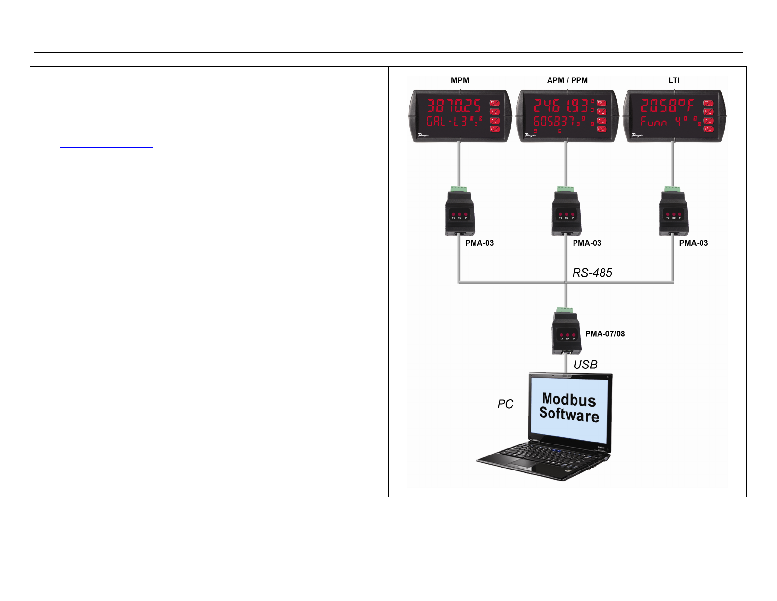
Introduction
This document describes how to communicate with the MPM, APM, PPM, or LTI Series
of meters using the Modbus
familiar with Modbus serial communication and the meters. Refer to the meter instruction
manual and the serial communication adapters’ manual for setup and wiring instructions.
Go to http://www.modbus.org/
Modbus Technical Resources.
Note that although there are no specific 3x Registers, all 4x Registers are mirrored into
3x register space, and are therefore capable of being read by Modbus function 04 (Read
Input Registers).
®
RTU Serial Communication Protocol. The user should be
to obtain a copy of the Modbus Specifications and to find
Register Overview
40001 – 40047: Process Value (PV), Max PV, Min PV, Total, and Grand Total in floating
point and long integer formats, with interspersed relay status & digital I/O
status, for block reading; Start & Stop batch, Relay acknowledge, Reset
Max & Min, Reset Total, Grand Total & Batch count.
40051 – 40089: Manual control of relays, analog output, and digital outputs; Modbus
input display settings to use the meter as a Modbus display.
40101 – 40125: Input selection, Decimal points, totalizer settings, display settings, and
display intensity.
40126 – 40145: Adjust, RTD number to average, Filter & Bypass, Gate settings for pulse
input, Serial communication settings, Transfer function, Number of
points, Exponent, Round horizontal tank parameters, and Cutoff.
40152 – 40180: Function keys, Digital I/O, Passwords.
40181 – 40187: Dual-scale model: PV2 settings and PV2 value, PV1 Percent.
40301 – 40372: Relays; Set & Reset points, Turn-on & Turn-off delays, Operating Mode.
40401 – 40413: Analog output value and setup parameters.
41001 – 41129: Remote Scaling for 4-20 mA input.
42001 – 42129: Remote Scaling for voltage input.
43001 – 43129: Remote Scaling for pulse input.
44001 – 44129: Remote Scaling for 4-20 mA input PV2.
45001 – 45129: Remote Scaling for voltage input PV2.
49901 – 49908: Product ID and Firmware Version.
49999: Load Factory Defaults
Page 3
Page 4
MPM, APM, PPM, & LTI Series Modbus® Register Tables Serial Communication
Register
1
Number Address (hex)
40001 – 40002
40003
40004
40005 – 40006
40007 – 40008
40009 – 40010
40011 – 40012
40013 – 40014
40015 – 40016
40017 – 40018
40019 – 40020
40021
40022
0 – 1
(0000 – 0001)
2
(0002)
3
(0003)
4 – 5
(0004 – 0005)
6 – 7
(0006 – 0007)
8-9
(0008 – 0009)
10 – 11
(000A – 000B)
12 – 13
(000C – 000D)
14 – 15
(000E – 000F)
16 – 17
(0010 – 0011)
18 – 19
(0012 – 0013)
20
(0014)
21
(0015)
Name Access
PV/Rate Display
value
Alarm and Relay
status
Digital Inputs and
Outputs status
Maximum Display
value
Minimum Display
value
Total value Read Only 0 to 999999999 User defined Floating point 03, 04
Grand Total value Read Only 0 to 999999999 User defined Floating point 03, 04
Total overflow
value
Total non-
overflow value
Grand Total
overflow value
Grand Total non-
overflow value
PV/Rate Display
value
PV/Rate Display
value
Read Only -99999 to 999999 User defined Floating point 03, 04
Read Only
Read Only
Read Only -99999 to 999999 User defined Floating point 03, 04
Read Only -99999 to 999999 User defined Floating point 03, 04
Read Only 0 to 999 User defined Floating point 03, 04
Read Only 0 to 999999 User defined Floating point 03, 04
Read Only 0 to 999 User defined Floating point 03, 04
Read Only 0 to 999999 User defined Floating point 03, 04
Read Only -99999 to 999999 User defined Long Hi 03, 04
Read Only User defined Long Lo 03, 04
Limits or
1 = In Alarm
energized
1 = Input selected
1 = Output active
Range
1 = relay
2
Units
None Word; Bits 03, 04
None Word; Bits 03, 04
Data
Type
3
Function
Code(s)
Comments
Represents the PV/Rate display value including the decimal
point. Under Range = -99999, Over Range = 999999, and
Open = -99999
Read alarm status and energized/non-energized status of
relays. Alm = Alarm. Rly = Relay.
15 14 13 12 11 10 9 8 7 6 5 4 3 2 1 0
Alm8 Alm7 Alm6 Alm5 Alm4 Alm3 Alm2 Alm1 Rly8 Rly7 Rly6 Rly5 Rly4 Rly3 Rly2 Rly
Read the state of the digital inputs and outputs.
15 14 13 12 11 10 9 8 7 6 5 4 3 2 1 0
DI 8 DI 7 DI 6 DI 5 DI 4 DI 3 DI 2 DI 1 DO8 DO7 DO6 DO5 DO4 DO3 DO2 DO
Represents the Maximum display value, including the decimal
point, since last power up or Max Value reset.
Represents the Minimum display value, including the decimal
point, since last power up or Min Value reset.
Represents the Total value, including the decimal point, since
last Total reset.
Represents the Grand Total value, including the decimal point,
since last Grand Total reset.
Represents the Total overflow value, since last Total reset.
Represents the Total non-overflow value, since last Total reset.
Represents the Grand Total overflow value, since last Grand
Total reset.
Represents the Grand Total non-overflow value, since last
Grand Total reset.
Represents the PV/Rate display value excluding the decimal
point. Decimal point setting in 40102.
Must be read with 40021.
1
1
Page 4
Page 5
MPM, APM, PPM, & LTI Series Modbus® Register Tables Serial Communication
1
Register
Number Address (hex)
Name Access
Limits or
Range
2
Units
Data
Type
3
Function
Code(s)
Comments
40023
40024
40025
40026
40027
40028
40029
40030
40031
40032
40033
40034
40035
40036
40037
40038
40039
22
(0016)
23
(0017)
24
(0018)
25
(0019)
26
(001A)
27
(001B)
28
(001C)
29
(001D)
30
(001E)
31
(001F)
32
(0020)
33
(0021)
34
(0022)
35
(0023)
36
(0024)
37
(0025)
38
(0026)
Alarm and Relay
status
Digital Inputs and
Outputs status
Maximum Display
value
Maximum Display
value
Minimum Display
value
Minimum Display
value
Total value Read Only 0 to 999999999 User defined Long Hi 03, 04
Total value Read Only User defined Long Lo 03, 04
Grand Total value Read Only 0 to 999999999 User defined Long Hi 03, 04
Grand Total value Read Only User defined Long Lo 03, 04
Total overflow
value
Total non-
overflow value
Total non-
overflow value
Grand Total
overflow value
Grand Total non-
overflow value
Grand Total non-
overflow value
Start Batch Write Only Not applicable None Bit 06, 16
Read Only
Read Only
Read Only -99999 to 999999 User defined Long Hi 03, 04
Read Only User defined Long Lo 03, 04
Read Only -99999 to 999999 User defined Long Hi 03, 04
Read Only User defined Long Lo 03, 04
Read Only 0 to 999 User defined Integer 03, 04
Read Only 0 to 999999 User defined Long Hi 03, 04
Read Only User defined Long Lo 03, 04
Read Only 0 to 999 User defined Integer 03, 04
Read Only 0 to 999999 User defined Long Hi 03, 04
Read Only User defined Long Lo 03, 04
1 = In Alarm
1 = relay
energized
1 = Input selected
1 = Output active
None Word; Bits 03, 04
None Word; Bits 03, 04
Mirror of 40003. Read alarm status and energized/nonenergized status of relays. Alm = Alarm. Rly = Relay.
15 14 13 12 11 10 9 8 7 6 5 4 3 2 1 0
Alm8 Alm7 Alm6 Alm5 Alm4 Alm3 Alm2 Alm1 Rly8 Rly7 Rly6 Rly5 Rly4 Rly3 Rly2 Rly
Mirror of 40004. Read the state of the digital inputs and outputs.
15 14 13 12 11 10 9 8 7 6 5 4 3 2 1 0
DI 8 DI 7 DI 6 DI 5 DI 4 DI 3 DI 2 DI 1 DO8 DO7 DO6 DO5 DO4 DO3 DO2 DO
Represents the Maximum display value, excluding the decimal
point, since last power up or Max Value reset.
Must be read with 40025.
Represents the Maximum display value, excluding the decimal
point, since last power up or Max Value reset.
Must be read with 40027.
Represents the Total value, excluding the decimal point, since
last Total reset. Decimal point setting in 40103.
Must be read with 40029.
Represents the Grand Total value, excluding the decimal point,
since last Total reset. Decimal point setting in 40104.
Must be read with 40031.
Represents the Total overflow value, since last Total reset.
Represents the Total non-overflow value, since last Total reset.
Must be read with 40034.
Represents the Grand Total overflow value, since last Grand
Total reset.
Represents the Grand Total non-overflow value, since last
Grand Total reset.
Must be read with 40037.
Set bit to 1 to start the batch process.
1
1
Page 5
Page 6
MPM, APM, PPM, & LTI Series Modbus® Register Tables Serial Communication
1
Register
Number Address (hex)
Name Access
Limits or
Range
2
Units
Data
Type
3
Function
Code(s)
Comments
40040
40041
40042
40043
40044
40045
40046
40047
40048
40049 – 40050
40051
39
(0027)
40
(0028)
41
(0029)
42
(002A)
43
(002B)
44
(002C)
45
(002D)
46
(002E)
47
(002F)
48 – 49
(0030 – 0031)
50
(0032)
Stop Batch Write Only Not applicable None Bit 06, 16
Alarm
Acknowledge
Reset Maximum
Display value
Reset Minimum
Display value
Reset Maximum
/Minimum Display
value
Reset Total value Write Only Not applicable None Bit 06, 16
Reset Grand
Total value
Reset Batch
Count value
Control Mode Read Write Not applicable None Bit
Write Only Not applicable None Word; Bits 06, 16
Write Only Not applicable None Bit 06, 16
Write Only Not applicable None Bit 06, 16
Write Only Not applicable None Bit 06, 16
Write Only Not applicable None Bit 06, 16
Write Only Not applicable None Bit 06, 16
03, 04,
06, 16
Set bit to 1 to pause the batch process; set bit to 1 again to stop
batch process.
Clear Relay n alarm condition. Set bit equal to 1 to
acknowledge. Only has effect on relays programmed to allow
manual acknowledging. Bits 0-7 mirror Bits 8-15, Alm = Alarm
15 14 13 12 11 10 9 8 7 6 5 4 3 2 1 0
Alm8 Alm7 Alm6 Alm5 Alm4 Alm3 Alm2 Alm1 Alm8 Alm7 Alm6 Alm5 Alm4 Alm3 Alm2 Alm
Set bit to 1 to reset the Maximum Display value.
Set bit to 1 to reset the Minimum Display value.
Set bit to 1 to reset the Maximum/ Minimum Display values.
Set bit to 1 to reset the Total value.
Set bit to 1 to reset the Grand Total value.
Set bit to 1 to reset the Batch Count value.
Reserved for future use.
Reserved for future use.
0 = auto, 1 = manual
1
40052
40053
40054
51
(0033)
52
(0034)
53
(0035)
Manual Control
Analog Output
Setting
Manual Control
Relay 1 Setting
Read Write 0 to 23999 μA Integer
Read Write Not applicable None Bit
03, 04,
06, 16
03, 04,
06, 16
Represents the Manual Control Analog Output value.
Note: Register 40051 must be set to 1 = manual mode for
registers 40052-40069 to take effect.
Reserved for future use.
Represents the Manual Control Relay 1 setting. 0 = off, 1 = on
Page 6
Page 7

MPM, APM, PPM, & LTI Series Modbus® Register Tables Serial Communication
1
Register
Number Address (hex)
Name Access
Limits or
Range
2
Units
Data
Type
3
Function
Code(s)
Comments
40055
40056
40057
40058
40059
40060
40061
40062
40063
40064
40065
40066
40067
40068
40069
40070
40071
54
(0036)
55
(0037)
56
(0038)
57
(0039)
58
(003A)
59
(003B)
60
(003C)
61
(003D)
62
(003E)
63
(003F)
64
(0040)
65
(0041)
66
(0042)
67
(0043)
68
(0044)
69
(0045)
70
(0046)
Manual Control
Relay 2 Setting
Manual Control
Relay 3 Setting
Manual Control
Relay 4 Setting
Manual Control
Relay 5 Setting
Manual Control
Relay 6 Setting
Manual Control
Relay 7 Setting
Manual Control
Relay 8 Setting
Manual Control
DO 1 Setting
Manual Control
DO 2 Setting
Manual Control
DO 3 Setting
Manual Control
DO 4 Setting
Manual Control
DO 5 Setting
Manual Control
DO 6 Setting
Manual Control
DO 7 Setting
Manual Control
DO 8 Setting
Modbus Big
Display Setting
Modbus Little
Display Setting
Read Write Not applicable None Bit
Read Write Not applicable None Bit
Read Write Not applicable None Bit
Read Write Not applicable None Bit
Read Write Not applicable None Bit
Read Write Not applicable None Bit
Read Write Not applicable None Bit
Read Write Not applicable None Bit
Read Write Not applicable None Bit
Read Write Not applicable None Bit
Read Write Not applicable None Bit
Read Write Not applicable None Bit
Read Write Not applicable None Bit
Read Write Not applicable None Bit
Read Write Not applicable None Bit
Read Write Not applicable None Bit
Read Write Not applicable None Bit
03, 04,
06, 16
03, 04,
06, 16
03, 04,
06, 16
03, 04,
06, 16
03, 04,
06, 16
03, 04,
06, 16
03, 04,
06, 16
03, 04,
06, 16
03, 04,
06, 16
03, 04,
06, 16
03, 04,
06, 16
03, 04,
06, 16
03, 04,
06, 16
03, 04,
06, 16
03, 04,
06, 16
03, 04,
06, 16
03, 04,
06, 16
Represents the Manual Control Relay 2 setting. 0 = off, 1 = on
Represents the Manual Control Relay 3 setting. 0 = off, 1 = on
Represents the Manual Control Relay 4 setting. 0 = off, 1 = on
Represents the Manual Control Relay 5 setting. 0 = off, 1 = on
Represents the Manual Control Relay 6 setting. 0 = off, 1 = on
Represents the Manual Control Relay 7 setting. 0 = off, 1 = on
Represents the Manual Control Relay 8 setting. 0 = off, 1 = on
Represents the Manual Control Digital Output 1 setting. 0 = off,
1 = on
Represents the Manual Control Digital Output 2 setting. 0 = off,
1 = on
Represents the Manual Control Digital Output 3 setting. 0 = off,
1 = on
Represents the Manual Control Digital Output 4 setting. 0 = off,
1 = on
Represents the Manual Control Digital Output 5 setting. 0 = off,
1 = on
Represents the Manual Control Digital Output 6 setting. 0 = off,
1 = on
Represents the Manual Control Digital Output 7 setting. 0 = off,
1 = on
Represents the Manual Control Digital Output 8 setting. 0 = off,
1 = on
Represents the Modbus Big Display setting.
0 = display based on register 40072-40073.
1 = display based on register 40076-40081.
Modbus display mode must be set to 18 in register 40117.
Represents the Modbus Little Display setting.
0 = display based on register 40074-40075.
1 = display based on register 40082-40087.
Modbus display mode must be set to 18 in register 40118.
Page 7
Page 8

MPM, APM, PPM, & LTI Series Modbus® Register Tables Serial Communication
1
Register
Number Address (hex)
Name Access
Limits or
Range
2
Units
Data
Type
3
Function
Code(s)
Comments
40072 – 40073
40074 – 40075
40076
40077
40078
40079
40080
40081
40082
40083
40084
71 – 72
(0047 – 0048)
73 – 74
(0049 – 004A)
75
(004B)
76
(004C)
77
(004D)
78
(004E)
79
(004F)
80
(0050)
81
(0051)
82
(0052)
83
(0053)
Modbus Big
Display value
Modbus Little
Display value
Modbus Big
Display MSD
value
Modbus Big
Display MSD-1
value
Modbus Big
Display MSD-2
value
Modbus Big
Display MSD-3
value
Modbus Big
Display MSD-4
value
Modbus Big
Display MSD-5
(LSD) value
Modbus Little
Display MSD
value
Modbus Little
Display MSD-1
value
Modbus Little
Display MSD-2
value
Read Write
Read Write
Read Write Not applicable None Byte
Read Write Not applicable None Byte
Read Write Not applicable None Byte
Read Write Not applicable None Byte
Read Write Not applicable None Byte
Read Write Not applicable None Byte
Read Write Not applicable None Byte
Read Write Not applicable None Byte
Read Write Not applicable None Byte
-99999 to
+999999
-99999 to
+999999
User defined
User defined
Long Hi
Long Lo
Long Hi
Long Lo
03, 04,
06, 16
03, 04,
06, 16
03, 04,
06, 16
03, 04,
06, 16
03, 04,
06, 16
03, 04,
06, 16
03, 04,
06, 16
03, 04,
06, 16
03, 04,
06, 16
03, 04,
06, 16
03, 04,
06, 16
Represents the Modbus Big display value excluding the decimal
point. Register 40088 contains the decimal point.
Set Register 40070 = 0, Register 40117 = 18
Represents the Modbus Little display value excluding the
decimal point. Register 40089 contains the decimal point.
Register 40071 = 0, Register 40118 = 18
Represents the Modbus Big Display MSD (Most Significant
Digit) value. The hex value represents the allowable ASCII
character, see Table 7.
Register 40117 = 18
Register 40070 = 1 for registers 40076-81.
Register 40088 contains the decimal point.
Represents the Modbus Big Display MSD-1 value. The hex
value represents the allowable ASCII character.
Represents the Modbus Big Display MSD-2 value. The hex
value represents the allowable ASCII character.
Represents the Modbus Big Display MSD-3 value. The hex
value represents the allowable ASCII character.
Represents the Modbus Big Display MSD-4 value. The hex
value represents the allowable ASCII character.
Represents the Modbus Big Display MSD-5 (which is the LSD)
value. The hex value represents the allowable ASCII character.
Represents the Modbus Little Display MSD (Most Significant
Digit) value. The hex value represents the allowable ASCII
character, see Table 7.
Register 40118 = 18
Register 40071 = 1 for registers 40082-87.
Register 40089 contains the decimal point.
Represents the Modbus Little Display MSD-1 value. The hex
value represents the allowable ASCII character.
Represents the Modbus Little Display MSD-2 value. The hex
value represents the allowable ASCII character.
Page 8
Page 9

MPM, APM, PPM, & LTI Series Modbus® Register Tables Serial Communication
1
Register
Number Address (hex)
Name Access
Limits or
Range
2
Units
Data
Type
3
Function
Code(s)
Comments
40085
40086
40087
40088
40089
40090
40091
40092
40093
40094
40095
40101
84
(0054)
85
(0055)
86
(0056)
87
(0057)
88
(0058)
89
(0059)
90
(005A)
91
(005B)
92
(005C)
93
(005D)
94
(005E)
100
(0064)
Modbus Little
Display MSD-3
value
Modbus Little
Display MSD-4
value
Modbus Little
Display MSD-5
(LSD) value
Modbus Big
Display decimal
point
Modbus Little
Display decimal
point
Level Meter Read Write Not applicable None Bit
Process Total Read Write Not applicable None Bit
Pulse Total Read Write Not applicable None Bit
Meter Model Read Only Not applicable None Integer
Relay & Digital IO
count
Analog Output Read Only Not applicable None Bit
Input Selection Read Write Not applicable None Word; bits
Read Write Not applicable None Byte
Read Write Not applicable None Byte
Read Write Not applicable None Byte
Read Write 0 to 5 None Integer
Read Write 0 to 5 None Integer
Read Only Not applicable None Word; bytes
03, 04,
06, 16
03, 04,
06, 16
03, 04,
06, 16
03, 04,
06, 16
03, 04,
06, 16
03, 04,
06, 16
03, 04,
06, 16
03, 04,
06, 16
03, 04,
06, 16
03, 04,
06, 16
03, 04,
06, 16
03, 04,
06, 16
Represents the Modbus Little Display MSD-3 value. The hex
value represents the allowable ASCII character.
Represents the Modbus Little Display MSD-4 value. The hex
value represents the allowable ASCII character.
Represents the Modbus Little Display MSD-5 (which is the
LSD) value. The hex value represents the allowable ASCII
character.
Selects based on number of digits to the right of the decimal
point (e.g. 0 = no decimal point and 5 = d.ddddd).
Register 40070 = 1 or 0
Selects based on number of digits to the right of the decimal
point (e.g. 0 = no decimal point and 5 = d.ddddd).
Register 40071 = 1 or 0
Represents the selection for LEVEL meter with dual scale for
PV1 and PV2. 0 = No, 1 = Yes
Represents the selection for Process Total.
0 = No, 1 = Yes
Represents the selection for Pulse Total.
0 = No, 1 = Yes
0 = Process/Temperature
1 = Process Total
2 = Pulse Total
3 = Dual-Input Process
Relay & Digital IO count
LSByte = Relay count (4 or 8)
MSByte = Digital IO count (0, 4, or 8)
Represents the analog output option
0 = Not installed
1 = Installed
See Table 1.
4 = Reserve
5 = Process Batch
6 = Pulse Batch
7 = No Module
Page 9
Page 10

MPM, APM, PPM, & LTI Series Modbus® Register Tables Serial Communication
1
Register
Number Address (hex)
40102
40103
40104
40105
40106 – 40107
40108
40109
40110
40111 – 40112
40113
40114
40115 – 40116
40117
40118
40119
40120
40121
101
(0065)
102
(0066)
103
(0067)
104
(0068)
105 – 106
(0069 – 006A)
107
(006B)
108
(006C)
109
(006D)
110 – 111
(006E – 006F)
112
(0070)
113
(0071)
114 – 115
(0072 – 0073)
116
(0074)
117
(0075)
118
(0076)
119
(0077)
120
(0078)
Name Access
PV/Rate decimal
point
Total decimal
point
Grand Total
decimal point
Total time base Read Write 0 to 4 None Integer
Total Conversion
Factor
Total Reset mode Read Write Not applicable None Bit
Total Reset Delay Read Write 0 to 9999
Grand Total time
base
Grand Total
Conversion
Factor
Grand Total
Reset mode
Grand Total
Reset Delay
Pulse K- Factor Read Write
Big Display
Setting
Little Display
Setting
Units 1 Read Write Not applicable None Byte
Units 2 Read Write Not applicable None Byte
Units 3 Read Write Not applicable None Byte
Read Write 0 to 7 None Integer
Read Write 0 to 5 None Integer
Read Write 0 to 5 None Integer
Read Write
Read Write 0 to 4 None Integer
Read Write
Read Write Not applicable None Bit
Read Write 0 to 9999
Read Write 0 to 20 None Integer
Read Write 0 to 23 None Integer
Limits or
0.00001 to
0.00001 to
0.00001 to
Range
999999
999999
999999
2
1/10 of Seconds
1/10 of Seconds
Units
None Floating point
(0 to 999.9)
None Floating point
(0 to 999.9)
None Floating point
Data
Type
Integer
Integer
3
Function
Code(s)
03, 04,
06, 16
03, 04,
06, 16
03, 04,
06, 16
03, 04,
06, 16
03, 04,
06, 16
03, 04,
06, 16
03, 04,
06, 16
03, 04,
06, 16
03, 04,
06, 16
03, 04,
06, 16
03, 04,
06, 16
03, 04,
06, 16
03, 04,
06, 16
03, 04,
06, 16
03, 04,
06, 16
03, 04,
06, 16
03, 04,
06, 16
Comments
Selects based on number of digits to the right of the decimal
point (e.g. 0 = no decimal point and 5 = d.ddddd), also
selections for Temp Decimal Point using 0 = dddd, 1 = dddd.d,
6 = dddd°u, and 7 = dddd.du, where “u” is the units (F or C).
Selects based on number of digits to the right of the decimal
point (e.g. 0 = no decimal point and 5 = d.ddddd).
Selects based on number of digits to the right of the decimal
point (e.g. 0 = no decimal point and 5 = d.ddddd).
0 = sec, 1 = min, 2 = hour, 3 = day
0 = auto, 1 = manual
0 = sec, 1 = min, 2 = hour, 3 = day
0 = auto, 1 = manual
See Table 2.
See Table 2.
Represents the Modbus Little Display MSD (Most Significant
Digit) value. The hex value represents the allowable ASCII
character.
Represents the Modbus Little Display MSD-1 value. The hex
value represents the allowable ASCII character.
Represents the Modbus Little Display MSD-2 value. The hex
value represents the allowable ASCII character.
Page 10
Page 11

MPM, APM, PPM, & LTI Series Modbus® Register Tables Serial Communication
1
Register
Number Address (hex)
Name Access
Limits or
Range
2
Units
Data
Type
3
Function
Code(s)
Comments
40122
40123
40124
40125
40126
40127
40128
40129
40130
40131
40132
40133
40134
40135
121
(0079)
122
(007A)
123
(007B)
124
(007C)
125
(007D)
126
(007E)
127
(007F)
128
(0080)
129
(0081)
130
(0082)
131
(0083)
132
(0084)
133
(0085)
134
(0086)
Units 4 Read Write Not applicable None Byte
Units 5 Read Write Not applicable None Byte
Units 6 Read Write Not applicable None Byte
Display Intensity Read Write 1 to 8 None Integer
Adjust Value Read Write -500 to 500 1/10 of °C or °F Integer
RTD Total Value Read Write 1 to 10 None Integer
Lo Gate Setting Read Write 1 to 999 None Integer
High Gate Setting Read Write 20 to 9999 None Integer
Filter Setting Read Write
Bypass Setting Read Write 2 to 999
Serial Address Read Write 1 to 247 None Integer
Serial Baud Rate Read Write 0 to 6 None Integer
Serial Transmit
Delay
Serial Parity Read Write 0 to 3 None Integer
Read Write 0 to 199 ms Integer
0, 2 to 199
or
202 to 250, 900
Unit-less Integer
Percent of full
scale or °F
Integer
03, 04,
06, 16
03, 04,
06, 16
03, 04,
06, 16
03, 04,
06, 16
03, 04,
06, 16
03, 04,
06, 16
03, 04,
06, 16
03, 04,
06, 16
03, 04,
06, 16
03, 04,
06, 16
03, 04,
06, 16
03, 04,
06, 16
03, 04,
06, 16
03, 04,
06, 16
Represents the Modbus Little Display MSD-3 value. The hex
value represents the allowable ASCII character.
Represents the Modbus Little Display MSD-4 value. The hex
value represents the allowable ASCII character.
Represents the Modbus Little Display MSD-5 (which is the
LSD) value. The hex value represents the allowable ASCII
character.
8 is the brightest level. Writing out of range data results in level
1 or 8.
Actually represents -50.0 to +50.0. Offset value is only applied
to temperature inputs. If Adjust is greater than 27.7°C and the
temperature units are switched to °F, it will be set to 50.0 (lower
than -27.7, set to -50.0).
Value represents the number of parallel RTDs connected to the
signal input. Any other value than these results in a setting of 1.
Actually represents 0.1 to 99.9 setting.
Actually represents 2.0 to 999.9 setting.
Display filtering. 0 = no filtering. 2 to 199 = old + ((new old)/Filter). For pulse input 900 = Hi-Speed, 202 to 250 = LoSpeed where the range is 2 to 50.
Actually represents 0.2 to 99.9. If the input steps greater than
the bypass value, it will be displayed immediately, with no
filtering occurring. The number represents percent of full-scale
for process inputs and °F for temperature inputs. No effect if
filter = 0.
Changes to this register are saved but don’t take effect until
next meter reset (Modbus command or power-up). Writing out
of range data results in an address of 247.
0 = 300, 1 = 600, 2 = 1200, 3 = 2400, 4 = 4800, 5 = 9600, &
6 = 19200. Changes to this register are saved but don’t take
effect until next meter reset (Modbus command or power-up).
Writing out of range data results in a baud rate of 2400.
Transmit delay to minimize collisions on the RS-485 network.
0 = None with 1 stop bit, 1 = None with 2 stop bits, 2 = Odd,
3 = Even. Changes to this register are saved but don’t take
effect until next meter re-initialization (Writing 0xFF00 to 40299
or power-up). Writing out of range data results in a parity setting
of Even.
Page 11
Page 12

MPM, APM, PPM, & LTI Series Modbus® Register Tables Serial Communication
1
Register
Number Address (hex)
40136
40137
40138
40139
40140 – 40141
40142 – 40143
40144 – 40145
40146
40147 – 40148
40149
40150 – 40151
40152
40153
40154
40155
135
(0087)
136
(0088)
137
(0089)
138
(008A)
139 – 140
(008B – 008C)
141 – 142
(008D – 008E)
143 – 144
(008F – 0090)
145
(0091)
146 – 147
(0092 – 0093)
148
(0094)
149 – 150
(0095 – 0096)
151
(0097)
152
(0098)
153
(0099)
154
(009A)
Name Access
Serial Byte-to-
Byte Timeout
Function Mode Read Write 0 to 3 None Integer
PV/Rate
Number of Points
Exponent Read Write 10001 to 29999 None Integer
Round Horizontal
Tank Diameter
Round Horizontal
Tank Length
Cutoff Read Write 0 to 999999 User defined Floating point
Total Count
Direction
Total Count
Preset
Grand Total
Count Direction
Grand Total
Count Preset
Programmable
User F1 Setting
Programmable
User F2 Setting
Programmable
User F3 Setting
Programmable
User Digital
Input 1 Setting
Read Write 0 to 254 1/100 of Seconds Integer
Read Write 2 to 32 None Integer
Read Write 0 to 999.999 Inches Floating point
Read Write 0 to 999.999 Inches Floating point
Read Write Not applicable None Bit
Read Write 0 to 999999999 User defined Floating point
Read Write Not applicable None Bit
Read Write 0 to 999999999 User defined Floating point
Read Write 0 to 39 User defined Integer
Read Write 0 to 39 User defined Integer
Read Write 0 to 39 User defined Integer
Read Write 0 to 43 User defined Integer
Limits or
Range
2
Units
Data
Type
3
Function
Code(s)
03, 04,
06, 16
03, 04,
06, 16
03, 04,
06, 16
03, 04,
06, 16
03, 04,
06, 16
03, 04,
06, 16
03, 04,
06, 16
03, 04,
06, 16
03, 04,
06, 16
03, 04,
06, 16
03, 04,
06, 16
03, 04,
06, 16
03, 04,
06, 16
03, 04,
06, 16
03, 04,
06, 16
Comments
This is the timeout between bytes of a Modbus frame. Note that
a value less than the minimum value for the present baud rate
cannot be saved. Minimums are: 300 baud = 0.06 sec,
600 = 0.03, 1200 = 0.02 and 0.01 for 2400 to 19200. Changes
to this register are saved but don’t take effect until next meter
reset (Modbus command or power-up). Writing out of range
data results in a timeout of 2.54 seconds.
0 = Linear, 1 = Square Root, 2 = Exponent, and 3 = Round
Horizontal Tank
This register is only used when register 40137 is set to Linear.
Actually represents 1.0001 to 2.9999.
Set register 40137 = 2
Decimal point is fixed. The unit of measure is inches; the
volume calculation is in US gallons. The display may be rescaled to represent the volume in any engineering units.
Represents the cutoff value.
0 = count up, 1 = count down
Same as 40302 – 40303 Relay 1 set point.
0 = count up, 1 = count down
See Table 3.
See Table 3.
See Table 3.
See Table 3.
Page 12
Page 13

MPM, APM, PPM, & LTI Series Modbus® Register Tables Serial Communication
1
Register
Number Address (hex)
Name Access
Limits or
Range
2
Units
Data
Type
3
Function
Code(s)
Comments
40156
40157
40158
40159
40160
40161
40162
40163
40164
40165
40166
40167
40168
155
(009B)
156
(009C)
157
(009D)
158
(009E)
159
(009F)
160
(00A0)
161
(00A1)
162
(00A2)
163
(00A3)
164
(00A4)
165
(00A5)
166
(00A6)
167
(00A7)
Programmable
User Digital
Input 2 Setting
Programmable
User Digital
Input 3 Setting
Programmable
User Digital
Input 4 Setting
Programmable
User Digital
Input 5 Setting
Programmable
User Digital
Input 6 Setting
Programmable
User Digital
Input 7 Setting
Programmable
User Digital
Input 8 Setting
Programmable
User Digital
Output 1 Setting
Programmable
User Digital
Output 2 Setting
Programmable
User Digital
Output 3 Setting
Programmable
User Digital
Output 4 Setting
Programmable
User Digital
Output 5 Setting
Programmable
User Digital
Output 6 Setting
Read Write 0 to 43 User defined Integer
Read Write 0 to 43 User defined Integer
Read Write 0 to 43 User defined Integer
Read Write 0 to 43 User defined Integer
Read Write 0 to 43 User defined Integer
Read Write 0 to 43 User defined Integer
Read Write 0 to 43 User defined Integer
Read Write 0 to 20 User defined Integer
Read Write 0 to 20 User defined Integer
Read Write 0 to 20 User defined Integer
Read Write 0 to 20 User defined Integer
Read Write 0 to 20 User defined Integer
Read Write 0 to 20 User defined Integer
03, 04,
06, 16
03, 04,
06, 16
03, 04,
06, 16
03, 04,
06, 16
03, 04,
06, 16
03, 04,
06, 16
03, 04,
06, 16
03, 04,
06, 16
03, 04,
06, 16
03, 04,
06, 16
03, 04,
06, 16
03, 04,
06, 16
03, 04,
06, 16
See Table 3.
See Table 3.
See Table 3.
See Table 3.
See Table 3.
See Table 3.
See Table 3.
See Table 3.
See Table 3.
See Table 3.
See Table 3.
See Table 3.
See Table 3.
Page 13
Page 14

MPM, APM, PPM, & LTI Series Modbus® Register Tables Serial Communication
1
Register
Number Address (hex)
Name Access
Limits or
Range
2
Units
Data
Type
3
Function
Code(s)
Comments
40169
40170
40171 – 40172
40173 – 40174
40175 – 40176
40177 – 40178
40179 – 40180
40181
40182
40183 – 40184
40185
40186
40187
40301
40302 – 40303
40304 – 40305
40306
168
(00A8)
169
(00A9)
170 – 171
(00AA-00AB)
172 – 173
(00AC-00AD)
174 – 175
(00AE-00AF)
176 – 177
(00B0 – 00B1)
178 – 179
(00B2 – 00B3)
180
(00B4)
181
(00B5)
182 – 183
(00B6 – 00B7)
184
(00B8)
185
(00B9)
186
(00BA)
300
(012C)
301 – 302
(012D – 012E)
303 – 304
(012F – 0130)
305
(0131)
Programmable
User Digital
Output 7 Setting
Programmable
User Digital
Output 8 Setting
Password 1 Read Write 000000 to 999999 None Floating point
Password 2 Read Write 000000 to 999999 None Floating point
Password 3 Read Write 000000 to 999999 None Floating point
Total Password Read Write 000000 to 999999 None Floating point
Grand Total
Password
PV2 Decimal
Point
PV2 Number of
Points
PV2 Display
Value
PV2 Display
value
PV2 Display
value
PV1% Display
value
Relay 1 Mode Read Write Not applicable None Word; bits
Relay 1
Set Point
Relay 1
Reset Point
Relay 1
On Delay
Read Write 0 to 20 User defined Integer
Read Write 0 to 20 User defined Integer
Read Write 000000 to 999999 None Floating point
Read Write 0 to 5 None Integer
Read Write 2 to 8 None Integer
Read Only -99999 to 999999 User defined Floating point 03, 04
Read Only -99999 to 999999 User defined Long Hi 03, 04
Read Only User defined Long Lo 03, 04
Read Only -100 to 100 User defined Integer 03, 04
Read Write -99999 to 999999 User defined Floating point
Read Write -99999 to 999999 User defined Floating point
Read Write 0 to 1999 1/10 of Seconds Integer
03, 04,
06, 16
03, 04,
06, 16
03, 04,
06, 16
03, 04,
06, 16
03, 04,
06, 16
03, 04,
06, 16
03, 04,
06, 16
03, 04,
06, 16
03, 04,
06, 16
03, 04,
06, 16
03, 04,
06, 16
03, 04,
06, 16
03, 04,
06, 16
See Table 3.
See Table 3.
See Note 4.
See Note 4.
See Note 4.
See Note 4.
See Note 4.
Selects based on number of digits to the right of the decimal
point (e.g. 0 = no decimal point and 5 = d.ddddd).
This register is only used when register 40137 is set to Linear.
Represents the PV2 display value including the decimal point.
Under Range = -99999, Over Range = 999999, and
Open = -99999
Represents the display value excluding the decimal point.
Decimal point setting in 40181.
Must be read with 40185.
Represents the PV1% display value.
See Table 4 for operating modes and bit assignments.
Page 14
Page 15

MPM, APM, PPM, & LTI Series Modbus® Register Tables Serial Communication
1
Register
Number Address (hex)
Name Access
Limits or
Range
2
Units
Data
Type
3
Function
Code(s)
Comments
40307
40308 – 40309
40310
40311 – 40312
40313 – 40314
40315
40316
40317 – 40318
40319
40320 – 40321
40322 – 40323
40324
40325
40326 – 40327
40328
40329 – 40330
40331 – 40332
40333
40334
306
(0132)
307 – 308
(0133 – 0134)
309
(0135)
310 – 311
(0136 – 0137)
312 – 313
(0138 – 0139)
314
(013A)
315
(013B)
316 – 317
(013C – 013D)
318
(013E)
319 – 320
(013F – 0140)
321 – 322
(0141 – 0142)
323
(0143)
324
(0144)
325 – 326
(0145 – 0146)
327
(0147)
328 – 329
(0148 – 0149)
330 – 331
(014A – 014B)
332
(014C)
333
(014D)
Relay 1
Off Delay
Relay 1 Sample
Time
Relay 2 Mode Read Write Not applicable None Word; bits
Relay 2
Set Point
Relay 2
Reset Point
Relay 2
On Delay
Relay 2
Off Delay
Relay 2 Sample
Time
Relay 3 Mode Read Write Not applicable None Word; bits
Relay 3
Set Point
Relay 3
Reset Point
Relay 3
On Delay
Relay 3
Off Delay
Relay 3 Sample
Time
Relay 4 Mode Read Write Not applicable None Word; bits
Relay 4
Set Point
Relay 4
Reset Point
Relay 4
On Delay
Relay 4
Off Delay
Read Write 0 to 1999 1/10 of Seconds Integer
Read Write 0 to 59999 1/10 of Seconds Floating point
Read Write -99999 to 999999 User defined Floating point
Read Write -99999 to 999999 User defined Floating point
Read Write 0 to 1999 1/10 of Seconds Integer
Read Write 0 to 1999 1/10 of Seconds Integer
Read Write 0 to 59999 1/10 of Seconds Floating point
Read Write -99999 to 999999 User defined Floating point
Read Write -99999 to 999999 User defined Floating point
Read Write 0 to 1999 1/10 of Seconds Integer
Read Write 0 to 1999 1/10 of Seconds Integer
Read Write 0 to 59999 1/10 of Seconds Floating point
Read Write -99999 to 999999 User defined Floating point
Read Write -99999 to 999999 User defined Floating point
Read Write 0 to 1999 1/10 of Seconds Integer
Read Write 0 to 1999 1/10 of Seconds Integer
03, 04,
06, 16
03, 04,
06, 16
03, 04,
06, 16
03, 04,
06, 16
03, 04,
06, 16
03, 04,
06, 16
03, 04,
06, 16
03, 04,
06, 16
03, 04,
06, 16
03, 04,
06, 16
03, 04,
06, 16
03, 04,
06, 16
03, 04,
06, 16
03, 04,
06, 16
03, 04,
06, 16
03, 04,
06, 16
03, 04,
06, 16
03, 04,
06, 16
03, 04,
06, 16
See Table 4 for operating modes and bit assignments.
See Table 4 for operating modes and bit assignments.
See Table 4 for operating modes and bit assignments.
Page 15
Page 16

MPM, APM, PPM, & LTI Series Modbus® Register Tables Serial Communication
1
Register
Number Address (hex)
Name Access
Limits or
Range
2
Units
Data
Type
3
Function
Code(s)
Comments
40335 – 40336
40337
40338 – 40339
40340 – 40341
40342
40343
40344 – 40345
40346
40347 – 40348
40349 – 40350
40351
40352
40353 – 40354
40355
40356 – 40357
40358 – 40359
40360
40361
40362 – 40363
334 – 335
(014E – 014F)
336
(0150)
337 – 338
(0151 – 0152)
339 – 340
(153 – 0154)
341
(0155)
342
(0156)
343 – 344
(0157 – 0158)
345
(0159)
346 – 347
(015A – 015B)
348 – 349
(015C – 015D)
350
(015E)
351
(015F)
352 – 353
(0160 – 0161)
354
(0162)
355 – 356
(0163 – 0164)
357 – 358
(0165 – 0166)
359
(0167)
360
(0168)
361 – 362
(0169 – 016A)
Relay 4 Sample
Time
Relay 5 Mode Read Write Not applicable None Word; bits
Relay 5
Set Point
Relay 5
Reset Point
Relay 5
On Delay
Relay 5
Off Delay
Relay 5 Sample
Time
Relay 6 Mode Read Write Not applicable None Word; bits
Relay 6
Set Point
Relay 6
Reset Point
Relay 6
On Delay
Relay 6
Off Delay
Relay 6 Sample
Time
Relay 7 Mode Read Write Not applicable None Word; bits
Relay 7
Set Point
Relay 7
Reset Point
Relay 7
On Delay
Relay 7
Off Delay
Relay 7 Sample
Time
Read Write 0 to 59999 1/10 of Seconds Floating point
Read Write -99999 to 999999 User defined Floating point
Read Write -99999 to 999999 User defined Floating point
Read Write 0 to 1999 1/10 of Seconds Integer
Read Write 0 to 1999 1/10 of Seconds Integer
Read Write 0 to 59999 1/10 of Seconds Floating point
Read Write -99999 to 999999 User defined Floating point
Read Write -99999 to 999999 User defined Floating point
Read Write 0 to 1999 1/10 of Seconds Integer
Read Write 0 to 1999 1/10 of Seconds Integer
Read Write 0 to 59999 1/10 of Seconds Floating point
Read Write -99999 to 999999 User defined Floating point
Read Write -99999 to 999999 User defined Floating point
Read Write 0 to 1999 1/10 of Seconds Integer
Read Write 0 to 1999 1/10 of Seconds Integer
Read Write 0 to 59999 1/10 of Seconds Floating point
03, 04,
06, 16
03, 04,
06, 16
03, 04,
06, 16
03, 04,
06, 16
03, 04,
06, 16
03, 04,
06, 16
03, 04,
06, 16
03, 04,
06, 16
03, 04,
06, 16
03, 04,
06, 16
03, 04,
06, 16
03, 04,
06, 16
03, 04,
06, 16
03, 04,
06, 16
03, 04,
06, 16
03, 04,
06, 16
03, 04,
06, 16
03, 04,
06, 16
03, 04,
06, 16
See Table 4 for operating modes and bit assignments.
See Table 4 for operating modes and bit assignments.
See Table 4 for operating modes and bit assignments.
Page 16
Page 17

MPM, APM, PPM, & LTI Series Modbus® Register Tables Serial Communication
1
Register
Number Address (hex)
Name Access
Limits or
Range
2
Units
Data
Type
3
Function
Code(s)
Comments
40364
40365 – 40366
40367 – 40368
40369
40370
40371 – 40372
40401
40402
40403
40404
40405
40406
40407
40408 – 40409
40410 – 40411
40412
40413
363
(016B)
364 – 365
(016C – 016D)
366 – 367
(016E – 016F)
368
(0170)
369
(0171)
370 – 371
(0172 – 0173)
400
(0190)
401
(0191)
402
(0192)
403
(0193)
404
(0194)
405
(0195)
406
(0196)
407 – 408
(0197 – 0198)
409 – 410
(0199 – 019A)
411
(019B)
412
(019C)
Relay 8 Mode Read Write Not applicable None Word; bits
Relay 8
Set Point
Relay 8
Reset Point
Relay 8
On Delay
Relay 8
Off Delay
Relay 8 Sample
Time
Analog Output
Value
Analog Output
Mode
Analog Output
Overrange value
Analog Output
Underrange value
Analog Output
Sensor Break
value
Analog Output
Maximum value
allowed
Analog Output
Minimum value
allowed
Analog Output
Display Value 1
Analog Output
Display Value 2
Analog Output
Output 1
Analog Output
Output 2
Read Write -99999 to 999999 User defined Floating point
Read Write -99999 to 999999 User defined Floating point
Read Write 0 to 1999 1/10 of Seconds Integer
Read Write 0 to 1999 1/10 of Seconds Integer
Read Write 0 to 59999 1/10 of Seconds Floating point
Read Only 0 to 23999 μA Integer 03, 04
Read Write 0 to 15 None Integer
Read Write 0 to 23999 μA Integer
Read Write 0 to 23999 μA Integer
Read Write 0 to 23999, 32000 μA Integer
Read Write 0 to 23999 μA Integer
Read Write 0 to 23999 μA Integer
Read Write -99999 to 999999 User defined Floating point
Read Write -99999 to 999999 User defined Floating point
Read Write 0 to 23999 μA Integer
Read Write 0 to 23999 μA Integer
03, 04,
06, 16
03, 04,
06, 16
03, 04,
06, 16
03, 04,
06, 16
03, 04,
06, 16
03, 04,
06, 16
03, 04,
06, 16
03, 04,
06, 16
03, 04,
06, 16
03, 04,
06, 16
03, 04,
06, 16
03, 04,
06, 16
03, 04,
06, 16
03, 04,
06, 16
03, 04,
06, 16
03, 04,
06, 16
See Table 4 for operating modes and bit assignments.
See Table 5 for selection of the 4-20mA output source.
Analog Output scaling is only saved to memory after receiving
the Output 2 – register 40413.
Page 17
Page 18

MPM, APM, PPM, & LTI Series Modbus® Register Tables Serial Communication
1
Register
Number Address (hex)
Name Access
Limits or
Range
2
Units
Data
Type
3
Function
Code(s)
Comments
41001 – 41002
41003 – 41004
41005 – 41006
41007 – 41008
41009 – 41010
41011 – 41012
41013 – 41014
41015 – 41016
41017 – 41018
41019 – 41020
41021 – 41022
41023 – 41024
41025 – 41026
41027 – 41028
41029 – 41030
41031 – 41032
41033 – 41034
41035 – 41036
41037 – 41038
1000 – 1001
(3E8 – 3E9)
1002 – 1003
(3EA – 3EB)
1004 – 1005
(3EC – 3ED)
1006 – 1007
(3EE – 3EF)
1008 – 1009
(3F0 – 3F1)
1010 – 1011
(3F2 – 3F3)
1012 – 1013
(3F4 – 3F5)
1014 – 1015
(3F6 – 3F7)
1016 – 1017
(3F8 – 3F9)
1018 – 1019
(3FA – 3FB)
1020 – 1021
(3FC – 3FD)
1022 – 1023
(3FE – 3FF)
1024 – 1025
(400 – 401)
1026 – 1027
(402 – 403)
1028 – 1029
(404 – 405)
1030 – 1031
(406 – 407)
1032 – 1033
(408 – 409)
1034 – 1035
(40A – 40B)
1036 – 1037
(40C – 40D)
Scale mA
Display 1
Scale mA
Display 2
Scale mA
Display 3
Scale mA
Display 4
Scale mA
Display 5
Scale mA
Display 6
Scale mA
Display 7
Scale mA
Display 8
Scale mA
Display 9
Scale mA
Display 10
Scale mA
Display 11
Scale mA
Display 12
Scale mA
Display 13
Scale mA
Display 14
Scale mA
Display 15
Scale mA
Display 16
Scale mA
Display 17
Scale mA
Display 18
Scale mA
Display 19
Read Write -99999 to 999999 User defined Floating point
Read Write -99999 to 999999 User defined Floating point
Read Write -99999 to 999999 User defined Floating point
Read Write -99999 to 999999 User defined Floating point
Read Write -99999 to 999999 User defined Floating point
Read Write -99999 to 999999 User defined Floating point
Read Write -99999 to 999999 User defined Floating point
Read Write -99999 to 999999 User defined Floating point
Read Write -99999 to 999999 User defined Floating point
Read Write -99999 to 999999 User defined Floating point
Read Write -99999 to 999999 User defined Floating point
Read Write -99999 to 999999 User defined Floating point
Read Write -99999 to 999999 User defined Floating point
Read Write -99999 to 999999 User defined Floating point
Read Write -99999 to 999999 User defined Floating point
Read Write -99999 to 999999 User defined Floating point
Read Write -99999 to 999999 User defined Floating point
Read Write -99999 to 999999 User defined Floating point
Read Write -99999 to 999999 User defined Floating point
03, 04,
06, 16
03, 04,
06, 16
03, 04,
06, 16
03, 04,
06, 16
03, 04,
06, 16
03, 04,
06, 16
03, 04,
06, 16
03, 04,
06, 16
03, 04,
06, 16
03, 04,
06, 16
03, 04,
06, 16
03, 04,
06, 16
03, 04,
06, 16
03, 04,
06, 16
03, 04,
06, 16
03, 04,
06, 16
03, 04,
06, 16
03, 04,
06, 16
03, 04,
06, 16
After all the Display and Input values have been sent, write
0xFF00 to register 41129.
Page 18
Page 19

MPM, APM, PPM, & LTI Series Modbus® Register Tables Serial Communication
1
Register
Number Address (hex)
Name Access
Limits or
Range
2
Units
Data
Type
3
Function
Code(s)
Comments
41039 – 41040
41041 – 41042
41043 – 41044
41045 – 41046
41047 – 41048
41049 – 41050
41051 – 41052
41053 – 41054
41055 – 41056
41057 – 41058
41059 – 41060
41061 – 41062
41063 – 41064
41065 – 41066
41067 – 41068
41069 – 41070
41071 – 41072
41073 – 41074
41075 – 41076
1038 – 1039
(40E – 40F)
1040 – 1041
(410 – 411)
1042 – 1043
(412 – 413)
1044 – 1045
(414 – 415)
1046 – 1047
(416 – 417)
1048 – 1049
(418 – 419)
1050 – 1051
(41A – 41B)
1052 – 1053
(41C – 41D)
1054 – 1055
(41E – 41F)
1056 – 1057
(420 – 421)
1058 – 1059
(422 – 423)
1060 – 1061
(424 – 425)
1062 – 1063
(426 – 427)
1064 – 1065
(428 – 429)
1066 – 1067
(42A – 42B)
1068 – 1069
(42C – 42D)
1070 – 1071
(42E – 42F)
1072 – 1073
(430 – 431)
1074 – 1075
(432 – 433)
Scale mA
Display 20
Scale mA
Display 21
Scale mA
Display 22
Scale mA
Display 23
Scale mA
Display 24
Scale mA
Display 25
Scale mA
Display 26
Scale mA
Display 27
Scale mA
Display 28
Scale mA
Display 29
Scale mA
Display 30
Scale mA
Display 31
Scale mA
Display 32
Scale mA
Input 1
Scale mA
Input 2
Scale mA
Input 3
Scale mA
Input 4
Scale mA
Input 5
Scale mA
Input 6
Read Write -99999 to 999999 User defined Floating point
Read Write -99999 to 999999 User defined Floating point
Read Write -99999 to 999999 User defined Floating point
Read Write -99999 to 999999 User defined Floating point
Read Write -99999 to 999999 User defined Floating point
Read Write -99999 to 999999 User defined Floating point
Read Write -99999 to 999999 User defined Floating point
Read Write -99999 to 999999 User defined Floating point
Read Write -99999 to 999999 User defined Floating point
Read Write -99999 to 999999 User defined Floating point
Read Write -99999 to 999999 User defined Floating point
Read Write -99999 to 999999 User defined Floating point
Read Write -99999 to 999999 User defined Floating point
Read Write -99.999 to 99.999 mA Floating point
Read Write -99.999 to 99.999 mA Floating point
Read Write -99.999 to 99.999 mA Floating point
Read Write -99.999 to 99.999 mA Floating point
Read Write -99.999 to 99.999 mA Floating point
Read Write -99.999 to 99.999 mA Floating point
03, 04,
06, 16
03, 04,
06, 16
03, 04,
06, 16
03, 04,
06, 16
03, 04,
06, 16
03, 04,
06, 16
03, 04,
06, 16
03, 04,
06, 16
03, 04,
06, 16
03, 04,
06, 16
03, 04,
06, 16
03, 04,
06, 16
03, 04,
06, 16
03, 04,
06, 16
03, 04,
06, 16
03, 04,
06, 16
03, 04,
06, 16
03, 04,
06, 16
03, 04,
06, 16
Page 19
Page 20

MPM, APM, PPM, & LTI Series Modbus® Register Tables Serial Communication
1
Register
Number Address (hex)
Name Access
Limits or
Range
2
Units
Data
Type
3
Function
Code(s)
Comments
41077 – 41078
41079 – 41080
41081 – 41082
41083 – 41084
41085 – 41086
41087 – 41088
41089 – 41090
41091 – 41092
41093 – 41094
41095 – 41096
41097 – 41098
41099 – 41100
41101 – 41102
41103 – 41104
41105 – 41106
41107 – 41108
41109 – 41110
41111 – 41112
41113 – 41114
1076 – 1077
(434 – 435)
1078 – 1079
(436 – 437)
1080 – 1081
(438 – 439)
1082 – 1083
(43A – 43B)
1084 – 1085
(43C – 43D)
1086 – 1087
(43E – 43F)
1088 – 1089
(440 – 441)
1090 – 1091
(442 – 443)
1092 – 1093
(444 – 445)
1094 – 1095
(446 – 447)
1096 – 1097
(448 – 449)
1098 – 1099
(44A – 44B)
1100 – 1101
(44C – 44D)
1102 – 1103
(44E – 44F)
1104 – 1105
(450 – 451)
1106 – 1107
(452 – 453)
1108 – 1109
(454 – 455)
1110 – 1111
(456 – 457)
1112 – 1113
(458 – 459)
Scale mA
Input 7
Scale mA
Input 8
Scale mA
Input 9
Scale mA
Input 10
Scale mA
Input 11
Scale mA
Input 12
Scale mA
Input 13
Scale mA
Input 14
Scale mA
Input 15
Scale mA
Input 16
Scale mA
Input 17
Scale mA
Input 18
Scale mA
Input 19
Scale mA
Input 20
Scale mA
Input 21
Scale mA
Input 22
Scale mA
Input 23
Scale mA
Input 24
Scale mA
Input 25
Read Write -99.999 to 99.999 mA Floating point
Read Write -99.999 to 99.999 mA Floating point
Read Write -99.999 to 99.999 mA Floating point
Read Write -99.999 to 99.999 mA Floating point
Read Write -99.999 to 99.999 mA Floating point
Read Write -99.999 to 99.999 mA Floating point
Read Write -99.999 to 99.999 mA Floating point
Read Write -99.999 to 99.999 mA Floating point
Read Write -99.999 to 99.999 mA Floating point
Read Write -99.999 to 99.999 mA Floating point
Read Write -99.999 to 99.999 mA Floating point
Read Write -99.999 to 99.999 mA Floating point
Read Write -99.999 to 99.999 mA Floating point
Read Write -99.999 to 99.999 mA Floating point
Read Write -99.999 to 99.999 mA Floating point
Read Write -99.999 to 99.999 mA Floating point
Read Write -99.999 to 99.999 mA Floating point
Read Write -99.999 to 99.999 mA Floating point
Read Write -99.999 to 99.999 mA Floating point
03, 04,
06, 16
03, 04,
06, 16
03, 04,
06, 16
03, 04,
06, 16
03, 04,
06, 16
03, 04,
06, 16
03, 04,
06, 16
03, 04,
06, 16
03, 04,
06, 16
03, 04,
06, 16
03, 04,
06, 16
03, 04,
06, 16
03, 04,
06, 16
03, 04,
06, 16
03, 04,
06, 16
03, 04,
06, 16
03, 04,
06, 16
03, 04,
06, 16
03, 04,
06, 16
Page 20
Page 21

MPM, APM, PPM, & LTI Series Modbus® Register Tables Serial Communication
1
Register
Number Address (hex)
Name Access
Limits or
Range
2
Units
Data
Type
3
Function
Code(s)
Comments
41115 – 41116
41117 – 41118
41119 – 41120
41121 – 41122
41123 – 41124
41125 – 41126
41127 – 41128
41129
42001 – 42002
42003 – 42004
42005 – 42006
42007 – 42008
42009 – 42010
42011 – 42012
42013 – 42014
42015 – 42016
42017 – 42018
42019 – 42020
1114 – 1115
(45A – 45B)
1116 – 1117
(45C – 45D)
1118 – 1119
(45E – 45F)
1120 – 1121
(460 – 461)
1122 – 1123
(462 – 463)
1124 – 1125
(464 – 465)
1126 – 1127
(466 – 467)
1128
(468)
2000 – 2001
(7D0 – 7D1)
2002 – 2003
(7D2 – 7D3)
2004 – 2005
(7D4 – 7D5)
2006 – 2007
(7D6 – 7D7)
2008 – 2009
(7D8 – 7D9)
2010 – 2011
(7DA – 7DB)
2012 – 2013
(7DC – 7DD)
2014 – 2015
(7DE – 7DF)
2016 – 2017
(7E0 – 7E1)
2018 – 2019
(7E2 – 7E3)
Scale mA
Input 26
Scale mA
Input 27
Scale mA
Input 28
Scale mA
Input 29
Scale mA
Input 30
Scale mA
Input 31
Scale mA
Input 32
Remote Scale mA
Flag
Scale Volts
Display 1
Scale Volts
Display 2
Scale Volts
Display 3
Scale Volts
Display 4
Scale Volts
Display 5
Scale Volts
Display 6
Scale Volts
Display 7
Scale Volts
Display 8
Scale Volts
Display 9
Scale Volts
Display 10
Read Write -99.999 to 99.999 mA Floating point
Read Write -99.999 to 99.999 mA Floating point
Read Write -99.999 to 99.999 mA Floating point
Read Write -99.999 to 99.999 mA Floating point
Read Write -99.999 to 99.999 mA Floating point
Read Write -99.999 to 99.999 mA Floating point
Read Write -99.999 to 99.999 mA Floating point
Write Only
Read Write -99999 to 999999 User defined Floating point
Read Write -99999 to 999999 User defined Floating point
Read Write -99999 to 999999 User defined Floating point
Read Write -99999 to 999999 User defined Floating point
Read Write -99999 to 999999 User defined Floating point
Read Write -99999 to 999999 User defined Floating point
Read Write -99999 to 999999 User defined Floating point
Read Write -99999 to 999999 User defined Floating point
Read Write -99999 to 999999 User defined Floating point
Read Write -99999 to 999999 User defined Floating point
0xFF00 to
execute remote
scaling.
None
Unsigned
integer
03, 04,
06, 16
03, 04,
06, 16
03, 04,
06, 16
03, 04,
06, 16
03, 04,
06, 16
03, 04,
06, 16
03, 04,
06, 16
06, 16
03, 04,
06, 16
03, 04,
06, 16
03, 04,
06, 16
03, 04,
06, 16
03, 04,
06, 16
03, 04,
06, 16
03, 04,
06, 16
03, 04,
06, 16
03, 04,
06, 16
03, 04,
06, 16
Used to remote scale the mA input. Caution! See Note 5.
After all the Display and Input values have been sent, write
0xFF00 to register 42129.
Page 21
Page 22

MPM, APM, PPM, & LTI Series Modbus® Register Tables Serial Communication
1
Register
Number Address (hex)
Name Access
Limits or
Range
2
Units
Data
Type
3
Function
Code(s)
Comments
42021 – 42022
42023 – 42024
42025 – 42026
42027 – 42028
42029 – 42030
42031 – 42032
42033 – 42034
42035 – 42036
42037 – 42038
42039 – 42040
42041 – 42042
42043 – 42044
42045 – 42046
42047 – 42048
42049 – 42050
42051 – 42052
42053 – 42054
42055 – 42056
42057 – 42058
2020 – 2021
(7E4 – 7E5)
2022 – 2023
(7E6 – 7E7)
2024 – 2025
(7E8 – 7E9)
2026 – 2027
(7EA – 7EB)
2028 – 2029
(7EC – 7ED)
2030 – 2031
(7EE – 7EF)
2032 – 2033
(7F0 – 7F1)
2034 – 2035
(7F2 – 7F3)
2036 – 2037
(7F4 – 7F5)
2038 – 2039
(7F6 – 7F7)
2040 – 2041
(7F8 – 7F9)
2042 – 2043
(7FA – 7FB)
2044 – 2045
(7FC – 7FD)
2046 – 2047
(7FE – 7FF)
2048 – 2049
(800 – 801)
2050 – 2051
(802 – 803)
2052 – 2053
(804 – 805)
2054 – 2055
(806 – 807)
2056 – 2057
(808 – 809)
Scale Volts
Display 11
Scale Volts
Display 12
Scale Volts
Display 13
Scale Volts
Display 14
Scale Volts
Display 15
Scale Volts
Display 16
Scale Volts
Display 17
Scale Volts
Display 18
Scale Volts
Display 19
Scale Volts
Display 20
Scale Volts
Display 21
Scale Volts
Display 22
Scale Volts
Display 23
Scale Volts
Display 24
Scale Volts
Display 25
Scale Volts
Display 26
Scale Volts
Display 27
Scale Volts
Display 28
Scale Volts
Display 29
Read Write -99999 to 999999 User defined Floating point
Read Write -99999 to 999999 User defined Floating point
Read Write -99999 to 999999 User defined Floating point
Read Write -99999 to 999999 User defined Floating point
Read Write -99999 to 999999 User defined Floating point
Read Write -99999 to 999999 User defined Floating point
Read Write -99999 to 999999 User defined Floating point
Read Write -99999 to 999999 User defined Floating point
Read Write -99999 to 999999 User defined Floating point
Read Write -99999 to 999999 User defined Floating point
Read Write -99999 to 999999 User defined Floating point
Read Write -99999 to 999999 User defined Floating point
Read Write -99999 to 999999 User defined Floating point
Read Write -99999 to 999999 User defined Floating point
Read Write -99999 to 999999 User defined Floating point
Read Write -99999 to 999999 User defined Floating point
Read Write -99999 to 999999 User defined Floating point
Read Write -99999 to 999999 User defined Floating point
Read Write -99999 to 999999 User defined Floating point
03, 04,
06, 16
03, 04,
06, 16
03, 04,
06, 16
03, 04,
06, 16
03, 04,
06, 16
03, 04,
06, 16
03, 04,
06, 16
03, 04,
06, 16
03, 04,
06, 16
03, 04,
06, 16
03, 04,
06, 16
03, 04,
06, 16
03, 04,
06, 16
03, 04,
06, 16
03, 04,
06, 16
03, 04,
06, 16
03, 04,
06, 16
03, 04,
06, 16
03, 04,
06, 16
Page 22
Page 23

MPM, APM, PPM, & LTI Series Modbus® Register Tables Serial Communication
1
Register
Number Address (hex)
Name Access
Limits or
Range
2
Units
Data
Type
3
Function
Code(s)
Comments
42059 – 42060
42061 – 42062
42063 – 42064
42065 – 42066
42067 – 42068
42069 – 42070
42071 – 42072
42073 – 42074
42075 – 42076
42077 – 42078
42079 – 42080
42081 – 42082
42083 – 42084
42085 – 42086
42087 – 42088
42089 – 42090
42091 – 42092
42093 – 42094
42095 – 42096
2058 – 2059
(80A – 80B)
2060 – 2061
(80C – 80D)
2062 – 2063
(80E – 80F)
2064 – 2065
(810 – 811)
2066 – 2067
(812 – 813)
2068 – 2069
(814 – 815)
2070 – 2071
(816 – 817)
2072 – 2073
(818 – 819)
2074 – 2075
(81A – 81B)
2076 – 2077
(81C – 81D)
2078 – 2079
(81E – 81F)
2080 – 2081
(820 – 821)
2082 – 2083
(822 – 823)
2084 – 2085
(824 – 825)
2086 – 2087
(826 – 827)
2088 – 2089
(828 – 829)
2090 – 2091
(82A – 82B)
2092 – 2093
(82C – 82D)
2094 – 2095
(82E – 82F)
Scale Volts
Display 30
Scale Volts
Display 31
Scale Volts
Display 32
Scale Volts
Input 1
Scale Volts
Input 2
Scale Volts
Input 3
Scale Volts
Input 4
Scale Volts
Input 5
Scale Volts
Input 6
Scale Volts
Input 7
Scale Volts
Input 8
Scale Volts
Input 9
Scale Volts
Input 10
Scale Volts
Input 11
Scale Volts
Input 12
Scale Volts
Input 13
Scale Volts
Input 14
Scale Volts
Input 15
Scale Volts
Input 16
Read Write -99999 to 999999 User defined Floating point
Read Write -99999 to 999999 User defined Floating point
Read Write -99999 to 999999 User defined Floating point
Read Write -99.999 to 99.999 Volt Floating point
Read Write -99.999 to 99.999 Volt Floating point
Read Write -99.999 to 99.999 Volt Floating point
Read Write -99.999 to 99.999 Volt Floating point
Read Write -99.999 to 99.999 Volt Floating point
Read Write -99.999 to 99.999 Volt Floating point
Read Write -99.999 to 99.999 Volt Floating point
Read Write -99.999 to 99.999 Volt Floating point
Read Write -99.999 to 99.999 Volt Floating point
Read Write -99.999 to 99.999 Volt Floating point
Read Write -99.999 to 99.999 Volt Floating point
Read Write -99.999 to 99.999 Volt Floating point
Read Write -99.999 to 99.999 Volt Floating point
Read Write -99.999 to 99.999 Volt Floating point
Read Write -99.999 to 99.999 Volt Floating point
Read Write -99.999 to 99.999 Volt Floating point
03, 04,
06, 16
03, 04,
06, 16
03, 04,
06, 16
03, 04,
06, 16
03, 04,
06, 16
03, 04,
06, 16
03, 04,
06, 16
03, 04,
06, 16
03, 04,
06, 16
03, 04,
06, 16
03, 04,
06, 16
03, 04,
06, 16
03, 04,
06, 16
03, 04,
06, 16
03, 04,
06, 16
03, 04,
06, 16
03, 04,
06, 16
03, 04,
06, 16
03, 04,
06, 16
Page 23
Page 24

MPM, APM, PPM, & LTI Series Modbus® Register Tables Serial Communication
1
Register
Number Address (hex)
Name Access
Limits or
Range
2
Units
Data
Type
3
Function
Code(s)
Comments
42097 – 42098
42099 – 42100
42101 – 42102
42103 – 42104
42105 – 42106
42107 – 42108
42109 – 42110
42111 – 42112
42113 – 42114
42115 – 42116
42117 – 42118
42119 – 42120
42121 – 42122
42123 – 42124
42125 – 42126
42127 – 42128
42129
43001 – 43002
2096 – 2097
(830 – 831)
2098 – 2099
(832 – 833)
2100 – 2101
(834 – 835)
2102 – 2103
(836 – 837)
2104 – 2105
(838 – 839)
2106 – 2107
(83A – 83B)
2108 – 2109
(83C – 83D)
2110 – 2111
(83E – 83F)
2112 – 2113
(840 – 841)
2114 – 2115
(842 – 843)
2116 – 2117
(844 – 845)
2118 – 2119
(846 – 847)
2120 – 2121
(848 – 849)
2122 – 2123
(84A – 84B)
2124 – 2125
(84C – 84D)
2126 – 2127
(84E – 84F)
2128
(850)
3000 – 3001
(BB8 – BB9)
Scale Volts
Input 17
Scale Volts
Input 18
Scale Volts
Input 19
Scale Volts
Input 20
Scale Volts
Input 21
Scale Volts
Input 22
Scale Volts
Input 23
Scale Volts
Input 24
Scale Volts
Input 25
Scale Volts
Input 26
Scale Volts
Input 27
Scale Volts
Input 28
Scale Volts
Input 29
Scale Volts
Input 30
Scale Volts
Input 31
Scale Volts
Input 32
Remote Scale
Volts Flag
Scale Pulse
Display 1
Read Write -99.999 to 99.999 Volt Floating point
Read Write -99.999 to 99.999 Volt Floating point
Read Write -99.999 to 99.999 Volt Floating point
Read Write -99.999 to 99.999 Volt Floating point
Read Write -99.999 to 99.999 Volt Floating point
Read Write -99.999 to 99.999 Volt Floating point
Read Write -99.999 to 99.999 Volt Floating point
Read Write -99.999 to 99.999 Volt Floating point
Read Write -99.999 to 99.999 Volt Floating point
Read Write -99.999 to 99.999 Volt Floating point
Read Write -99.999 to 99.999 Volt Floating point
Read Write -99.999 to 99.999 Volt Floating point
Read Write -99.999 to 99.999 Volt Floating point
Read Write -99.999 to 99.999 Volt Floating point
Read Write -99.999 to 99.999 Volt Floating point
Read Write -99.999 to 99.999 Volt Floating point
Write Only
Read Write -99999 to 999999 User defined Floating point
0xFF00 to
execute remote
scaling.
None
Unsigned
integer
03, 04,
06, 16
03, 04,
06, 16
03, 04,
06, 16
03, 04,
06, 16
03, 04,
06, 16
03, 04,
06, 16
03, 04,
06, 16
03, 04,
06, 16
03, 04,
06, 16
03, 04,
06, 16
03, 04,
06, 16
03, 04,
06, 16
03, 04,
06, 16
03, 04,
06, 16
03, 04,
06, 16
03, 04,
06, 16
06, 16
03, 04,
06, 16
Used to remote scale the Volt input. Caution! See Note 5.
After all the Display and Input values have been sent, write
0xFF00 to register 43129.
Page 24
Page 25

MPM, APM, PPM, & LTI Series Modbus® Register Tables Serial Communication
1
Register
Number Address (hex)
Name Access
Limits or
Range
2
Units
Data
Type
3
Function
Code(s)
Comments
43003 – 43004
43005 – 43006
43007 – 43008
43009 – 43010
43011 – 43012
43013 – 43014
43015 – 43016
43017 – 43018
43019 – 43020
43021 – 43022
43023 – 43024
43025 – 43026
43027 – 43028
43029 – 43030
43031 – 43032
43033 – 43034
43035 – 43036
43037 – 43038
43039 – 43040
3002 – 3003
(BBA – BBB)
3004 – 3005
(BBC – BBD)
3006 – 3007
(BBE – BBF)
3008 – 3009
(BC0 – BC1)
3010 – 3011
(BC2 – BC3)
3012 – 3013
(BC4 – BC5)
3014 – 3015
(BC6 – BC7)
3016 – 3017
(BC8 – BC9)
3018 – 3019
(BCA – BCB)
3020 – 3021
(BCC – BCD)
3022 – 3023
(BCE – BCF)
3024 – 3025
(BD0 – BD1)
3026 – 3027
(BD2 – BD3)
3028 – 3029
(BD4 – BD5)
3030 – 3031
(BD6 – BD7)
3032 – 3033
(BD8 – BD9)
3034 – 3035
(BDA – BDB)
3036 – 3037
(BDC – BDD)
3038 – 3039
(BDE – BDF)
Scale Pulse
Display 2
Scale Pulse
Display 3
Scale Pulse
Display 4
Scale Pulse
Display 5
Scale Pulse
Display 6
Scale Pulse
Display 7
Scale Pulse
Display 8
Scale Pulse
Display 9
Scale Pulse
Display 10
Scale Pulse
Display 11
Scale Pulse
Display 12
Scale Pulse
Display 13
Scale Pulse
Display 14
Scale Pulse
Display 15
Scale Pulse
Display 16
Scale Pulse
Display 17
Scale Pulse
Display 18
Scale Pulse
Display 19
Scale Pulse
Display 20
Read Write -99999 to 999999 User defined Floating point
Read Write -99999 to 999999 User defined Floating point
Read Write -99999 to 999999 User defined Floating point
Read Write -99999 to 999999 User defined Floating point
Read Write -99999 to 999999 User defined Floating point
Read Write -99999 to 999999 User defined Floating point
Read Write -99999 to 999999 User defined Floating point
Read Write -99999 to 999999 User defined Floating point
Read Write -99999 to 999999 User defined Floating point
Read Write -99999 to 999999 User defined Floating point
Read Write -99999 to 999999 User defined Floating point
Read Write -99999 to 999999 User defined Floating point
Read Write -99999 to 999999 User defined Floating point
Read Write -99999 to 999999 User defined Floating point
Read Write -99999 to 999999 User defined Floating point
Read Write -99999 to 999999 User defined Floating point
Read Write -99999 to 999999 User defined Floating point
Read Write -99999 to 999999 User defined Floating point
Read Write -99999 to 999999 User defined Floating point
03, 04,
06, 16
03, 04,
06, 16
03, 04,
06, 16
03, 04,
06, 16
03, 04,
06, 16
03, 04,
06, 16
03, 04,
06, 16
03, 04,
06, 16
03, 04,
06, 16
03, 04,
06, 16
03, 04,
06, 16
03, 04,
06, 16
03, 04,
06, 16
03, 04,
06, 16
03, 04,
06, 16
03, 04,
06, 16
03, 04,
06, 16
03, 04,
06, 16
03, 04,
06, 16
Page 25
Page 26

MPM, APM, PPM, & LTI Series Modbus® Register Tables Serial Communication
1
Register
Number Address (hex)
Name Access
Limits or
Range
2
Units
Data
Type
3
Function
Code(s)
Comments
43041 – 43042
43043 – 43044
43045 – 43046
43047 – 43048
43049 – 43050
43051 – 43052
43053 – 43054
43055 – 43056
43057 – 43058
43059 – 43060
43061 – 43062
43063 – 43064
43065 – 43066
43067 – 43068
43069 – 43070
43071 – 43072
43073 – 43074
43075 – 43076
43077 – 43078
3040 – 3041
(BE0 – BE1)
3042 – 3043
(BE2 – BE3)
3044 – 3045
(BE4 – BE5)
3046 – 3047
(BE6 – BE7)
3048 – 3049
(BE8 – BE9)
3050 – 3051
(BEA – BEB)
3052 – 3053
(BEC – BED)
3054 – 3055
(BEE – BEF)
3056 – 3057
(BF0 – BF1)
3058 – 3059
(BF2 – BF3)
3060 – 3061
(BF4 – BF5)
3062 – 3063
(BF6 – BF7)
3064 – 3065
(BF8 – BF9)
3066 – 3067
(BFA – BFB)
3068 – 3069
(BFC – BFD)
3070 – 3071
(BFE – BFF)
3072 – 3073
(C00 – C01)
3074 – 3075
(C02 – C03)
3076 – 3077
(C04 – C05)
Scale Pulse
Display 21
Scale Pulse
Display 22
Scale Pulse
Display 23
Scale Pulse
Display 24
Scale Pulse
Display 25
Scale Pulse
Display 26
Scale Pulse
Display 27
Scale Pulse
Display 28
Scale Pulse
Display 29
Scale Pulse
Display 30
Scale Pulse
Display 31
Scale Pulse
Display 32
Scale Pulse
Input 1
Scale Pulse
Input 2
Scale Pulse
Input 3
Scale Pulse
Input 4
Scale Pulse
Input 5
Scale Pulse
Input 6
Scale Pulse
Input 7
Read Write -99999 to 999999 User defined Floating point
Read Write -99999 to 999999 User defined Floating point
Read Write -99999 to 999999 User defined Floating point
Read Write -99999 to 999999 User defined Floating point
Read Write -99999 to 999999 User defined Floating point
Read Write -99999 to 999999 User defined Floating point
Read Write -99999 to 999999 User defined Floating point
Read Write -99999 to 999999 User defined Floating point
Read Write -99999 to 999999 User defined Floating point
Read Write -99999 to 999999 User defined Floating point
Read Write -99999 to 999999 User defined Floating point
Read Write -99999 to 999999 User defined Floating point
Read Write 0.0 to 99999.9 Hz Floating point
Read Write 0.0 to 99999.9 Hz Floating point
Read Write 0.0 to 99999.9 Hz Floating point
Read Write 0.0 to 99999.9 Hz Floating point
Read Write 0.0 to 99999.9 Hz Floating point
Read Write 0.0 to 99999.9 Hz Floating point
Read Write 0.0 to 99999.9 Hz Floating point
03, 04,
06, 16
03, 04,
06, 16
03, 04,
06, 16
03, 04,
06, 16
03, 04,
06, 16
03, 04,
06, 16
03, 04,
06, 16
03, 04,
06, 16
03, 04,
06, 16
03, 04,
06, 16
03, 04,
06, 16
03, 04,
06, 16
03, 04,
06, 16
03, 04,
06, 16
03, 04,
06, 16
03, 04,
06, 16
03, 04,
06, 16
03, 04,
06, 16
03, 04,
06, 16
Page 26
Page 27

MPM, APM, PPM, & LTI Series Modbus® Register Tables Serial Communication
1
Register
Number Address (hex)
Name Access
Limits or
Range
2
Units
Data
Type
3
Function
Code(s)
Comments
43079 – 43080
43081 – 43082
43083 – 43084
43085 – 43086
43087 – 43088
43089 – 43090
43091 – 43092
43093 – 43094
43095 – 43096
43097 – 43098
43099 – 43100
43101 – 43102
43103 – 43104
43105 – 43106
43107 – 43108
43109 – 43110
43111 – 43112
43113 – 43114
43115 – 43116
3078 – 3079
(C06 – C07)
3080 – 3081
(C08 – C09)
3082 – 3083
(C0A – C0B)
3084 – 3085
(C0C – C0D)
3086 – 3087
(C0E – C0F)
3088 – 3089
(C10 – C11)
3090 – 3091
(C12 – C13)
3092 – 3093
(C14 – C15)
3094 – 3095
(C16 – C17)
3096 – 3097
(C18 – C19)
3098 – 3099
(C1A – C1B)
3100 – 3101
(C1C – C1D)
3102 – 3103
(C1E – C1F)
3104 – 3105
(C20 – C21)
3106 – 3107
(C22 – C23)
3108 – 3109
(C24 – C25)
3110 – 3111
(C26 – C27)
3112 – 3113
(C28 – C29)
3114 – 3115
(C2A – C2B)
Scale Pulse
Input 8
Scale Pulse
Input 9
Scale Pulse
Input 10
Scale Pulse
Input 11
Scale Pulse
Input 12
Scale Pulse
Input 13
Scale Pulse
Input 14
Scale Pulse
Input 15
Scale Pulse
Input 16
Scale Pulse
Input 17
Scale Pulse
Input 18
Scale Pulse
Input 19
Scale Pulse
Input 20
Scale Pulse
Input 21
Scale Pulse
Input 22
Scale Pulse
Input 23
Scale Pulse
Input 24
Scale Pulse
Input 25
Scale Pulse
Input 26
Read Write 0.0 to 99999.9 Hz Floating point
Read Write 0.0 to 99999.9 Hz Floating point
Read Write 0.0 to 99999.9 Hz Floating point
Read Write 0.0 to 99999.9 Hz Floating point
Read Write 0.0 to 99999.9 Hz Floating point
Read Write 0.0 to 99999.9 Hz Floating point
Read Write 0.0 to 99999.9 Hz Floating point
Read Write 0.0 to 99999.9 Hz Floating point
Read Write 0.0 to 99999.9 Hz Floating point
Read Write 0.0 to 99999.9 Hz Floating point
Read Write 0.0 to 99999.9 Hz Floating point
Read Write 0.0 to 99999.9 Hz Floating point
Read Write 0.0 to 99999.9 Hz Floating point
Read Write 0.0 to 99999.9 Hz Floating point
Read Write 0.0 to 99999.9 Hz Floating point
Read Write 0.0 to 99999.9 Hz Floating point
Read Write 0.0 to 99999.9 Hz Floating point
Read Write 0.0 to 99999.9 Hz Floating point
Read Write 0.0 to 99999.9 Hz Floating point
03, 04,
06, 16
03, 04,
06, 16
03, 04,
06, 16
03, 04,
06, 16
03, 04,
06, 16
03, 04,
06, 16
03, 04,
06, 16
03, 04,
06, 16
03, 04,
06, 16
03, 04,
06, 16
03, 04,
06, 16
03, 04,
06, 16
03, 04,
06, 16
03, 04,
06, 16
03, 04,
06, 16
03, 04,
06, 16
03, 04,
06, 16
03, 04,
06, 16
03, 04,
06, 16
Page 27
Page 28

MPM, APM, PPM, & LTI Series Modbus® Register Tables Serial Communication
1
Register
Number Address (hex)
Name Access
Limits or
Range
2
Units
Data
Type
3
Function
Code(s)
Comments
43117 – 43118
43119 – 43120
43121 – 43122
43123 – 43124
43125 – 43126
43127 – 43128
43129
44001 – 44002
44003 – 44004
44005 – 44006
44007 – 44008
44009 – 44010
44011 – 44012
44013 – 44014
44015 – 44016
44017 – 44018
44019 – 44020
44021 – 44022
3116 – 3117
(C2C – C2D)
3118 – 3119
(C2E – C2F)
3120 – 3121
(C30 – C31)
3122 – 3123
(C32 – C33)
3124 – 3125
(C34 – C35)
3126 – 3127
(C36 – C37)
3128
(C38)
4000 – 4001
(FA0 – FA1)
4002 – 4003
(FA2 – FA3)
4004 – 4005
(FA4 – FA5)
4006 – 4007
(FA6 – FA7)
4008 – 4009
(FA8 – FA9)
4010 – 4011
(FAA – FAB)
4012 – 4013
(FAC – FAD)
4014 – 4015
(FAE – FAF)
4016 – 4017
(FB0 – FB1)
4018 – 4019
(FB2 – FB3)
4020 – 4021
(FB4 – FB5)
Scale Pulse
Input 27
Scale Pulse
Input 28
Scale Pulse
Input 29
Scale Pulse
Input 30
Scale Pulse
Input 31
Scale Pulse
Input 32
Remote Scale
Pulse Flag
Scale PV2 mA
Display 1
Scale PV2 mA
Display 2
Scale PV2 mA
Display 3
Scale PV2 mA
Display 4
Scale PV2 mA
Display 5
Scale PV2 mA
Display 6
Scale PV2 mA
Display 7
Scale PV2 mA
Display 8
Scale PV2 mA
Input 1
Scale PV2 mA
Input 2
Scale PV2 mA
Input 3
Read Write 0.0 to 99999.9 Hz Floating point
Read Write 0.0 to 99999.9 Hz Floating point
Read Write 0.0 to 99999.9 Hz Floating point
Read Write 0.0 to 99999.9 Hz Floating point
Read Write 0.0 to 99999.9 Hz Floating point
Read Write 0.0 to 99999.9 Hz Floating point
Write Only
Read Write -99999 to 999999 User defined Floating point
Read Write -99999 to 999999 User defined Floating point
Read Write -99999 to 999999 User defined Floating point
Read Write -99999 to 999999 User defined Floating point
Read Write -99999 to 999999 User defined Floating point
Read Write -99999 to 999999 User defined Floating point
Read Write -99999 to 999999 User defined Floating point
Read Write -99999 to 999999 User defined Floating point
Read Write -99.999 to 99.999 mA Floating point
Read Write -99.999 to 99.999 mA Floating point
Read Write -99.999 to 99.999 mA Floating point
0xFF00 to
execute remote
scaling.
None
Unsigned
integer
03, 04,
06, 16
03, 04,
06, 16
03, 04,
06, 16
03, 04,
06, 16
03, 04,
06, 16
03, 04,
06, 16
06, 16
03, 04,
06, 16
03, 04,
06, 16
03, 04,
06, 16
03, 04,
06, 16
03, 04,
06, 16
03, 04,
06, 16
03, 04,
06, 16
03, 04,
06, 16
03, 04,
06, 16
03, 04,
06, 16
03, 04,
06, 16
Used to remote scale the Pulse input. Caution! See Note 5.
After all the Display and Input values have been sent, write
0xFF00 to register 44129.
Page 28
Page 29

MPM, APM, PPM, & LTI Series Modbus® Register Tables Serial Communication
1
Register
Number Address (hex)
Name Access
Limits or
Range
2
Units
Data
Type
3
Function
Code(s)
Comments
44023 – 44024
44025 – 44026
44027 – 44028
44029 – 44030
44031 – 44032
44129
45001 – 45002
45003 – 45004
45005 – 45006
45007 – 45008
45009 – 45010
45011 – 45012
45013 – 45014
45015 – 45016
45017 – 45018
45019 – 45020
45021 – 45022
45023 – 45024
4022 – 4023
(FB6 – FB7)
4024 – 4025
(FB8 – FB9)
4026 – 4027
(FBA – FBB)
4028 – 4029
(FBC – FBD)
4030 – 4031
(FBE – FBF)
4128
(1020)
5000 – 5001
(1388 – 1389)
5002 – 5003
(138A – 138B)
5004 – 5005
(138C – 138D)
5006 – 5007
(138E – 138F)
5008 – 5009
(1390 – 1391)
5010 – 5011
(1392 – 1393)
5012 – 5013
(1394 – 1395)
5014 – 5015
(1396 – 1397)
5016 – 5017
(1398 – 1399)
5018 – 5019
(139A – 139B)
5020 – 5021
(139C – 139D)
5022 – 5023
(139E – 139F)
Scale PV2 mA
Input 4
Scale PV2 mA
Input 5
Scale PV2 mA
Input 6
Scale PV2 mA
Input 7
Scale PV2 mA
Input 8
Remote Scale
PV2 mA Flag
Scale PV2 Volts
Display 1
Scale PV2 Volts
Display 2
Scale PV2 Volts
Display 3
Scale PV2 Volts
Display 4
Scale PV2 Volts
Display 5
Scale PV2 Volts
Display 6
Scale PV2 Volts
Display 7
Scale PV2 Volts
Display 8
Scale PV2 Volts
Input 1
Scale PV2 Volts
Input 2
Scale PV2 Volts
Input 3
Scale PV2 Volts
Input 4
Read Write -99.999 to 99.999 mA Floating point
Read Write -99.999 to 99.999 mA Floating point
Read Write -99.999 to 99.999 mA Floating point
Read Write -99.999 to 99.999 mA Floating point
Read Write -99.999 to 99.999 mA Floating point
Write Only
Read Write -99999 to 999999 User defined Floating point
Read Write -99999 to 999999 User defined Floating point
Read Write -99999 to 999999 User defined Floating point
Read Write -99999 to 999999 User defined Floating point
Read Write -99999 to 999999 User defined Floating point
Read Write -99999 to 999999 User defined Floating point
Read Write -99999 to 999999 User defined Floating point
Read Write -99999 to 999999 User defined Floating point
Read Write -99.999 to 99.999 Volt Floating point
Read Write -99.999 to 99.999 Volt Floating point
Read Write -99.999 to 99.999 Volt Floating point
Read Write -99.999 to 99.999 Volt Floating point
0xFF00 to
execute remote
scaling.
None
Unsigned
integer
03, 04,
06, 16
03, 04,
06, 16
03, 04,
06, 16
03, 04,
06, 16
03, 04,
06, 16
06, 16
03, 04,
06, 16
03, 04,
06, 16
03, 04,
06, 16
03, 04,
06, 16
03, 04,
06, 16
03, 04,
06, 16
03, 04,
06, 16
03, 04,
06, 16
03, 04,
06, 16
03, 04,
06, 16
03, 04,
06, 16
03, 04,
06, 16
Used to remote scale the PV2 mA input. Caution! See Note 5.
After all the Display and Input values have been sent, write
0xFF00 to register 45129.
Page 29
Page 30

MPM, APM, PPM, & LTI Series Modbus® Register Tables Serial Communication
1
Register
Number Address (hex)
Name Access
Limits or
Range
2
Units
Data
Type
3
Function
Code(s)
Comments
45025 – 45026
45027 – 45028
45029 – 45030
45031 – 45032
45129
49901 – 49904
49905 – 49908
49999
5024 – 5025
(13A0 – 13A1)
5026 – 5027
(13A2 – 13A3)
5028 – 5029
(13A4 – 13A5)
5030 – 5031
(13A6 – 13A7)
5128
(1408)
9900-9903
(26AC – 26AF)
9904-9907
(26B0 – 26B3)
9998
(270E)
Scale PV2 Volts
Input 5
Scale PV2 Volts
Input 6
Scale PV2 Volts
Input 7
Scale PV2 Volts
Input 8
Remote Scale
PV2 Volts Flag
Product Identifier Read Only Not applicable None
Firmware Version Read Only Not applicable None
Load Factory
Defaults
Read Write -99.999 to 99.999 Volt Floating point
Read Write -99.999 to 99.999 Volt Floating point
Read Write -99.999 to 99.999 Volt Floating point
Read Write -99.999 to 99.999 Volt Floating point
Write Only
Write Only
0xFF00 to
execute remote
scaling.
0xFF00 to
initialize
None
None
Unsigned
integer
ASCII
characters
ASCII
characters
Unsigned
integer
03, 04,
06, 16
03, 04,
06, 16
03, 04,
06, 16
03, 04,
06, 16
06, 16
03, 04
03, 04
06, 16
Used to remote scale the PV2 Volts input. Caution! See Note 5.
8 characters indicating the product digit software release
number (for SFT039 this would be 039), three ASCII hex
character value of the Main board input, and two ASCII hex
characters of the Input card (see Table 6).
8 characters indicating the firmware version number
Write 0xFF00 to load factory defaults to the meter. Writing any
other data has no effect.
Page 30
Page 31

MPM, APM, PPM, & LTI Series Modbus® Register Tables Serial Communication
Notes
Note 1. The Register numbers and addresses follow the Modbus format:
3xxxx are for Input Registers and are read – only.
4xxxx are for Holding Registers and are read/write.
Although there are no specific 3x Registers, all 4x Registers are mirrored
into 3x register space, and are therefore capable of being read by
Modbus function 04 (Read Input Registers). All data addresses in
Modbus messages are referenced to zero (0), while Register addresses
are referenced to one (1). For example, Register 40100 is sent in the
Modbus message as 0x0063 (100 - 1 = 99 ≡ 63 hex). If two addresses
are shown separated by a “ – ”, they form a register pair to make the
parameter into a 4-byte (32 bit) value.
Note 2. Limits or Range: Writing a value that is outside the parameters range will
force it to be limited to the closest value within the range. For example, if
the range is -1.99 to +1.99 and the value sent is 3.21, the value used is
1.99. Likewise for the lower side of the range. Exceptions are noted in
the comments.
Note 3. Data Types:
Data format is highest byte first.
Word = 16 bit
Integer = -32768 to 32767
Unsigned integer = 0 to 65535
Long = -2,147,483,648 to 2,147,483,647
Float = IEEE floating point format, 4 bytes
Integers data: The values represent the number without regard to the
decimal point. The decimal point setting can be found in Holding
Register 40102.
For example, if the number 1234.56 is displayed, a read of both 40021 –
40022 together will return 1 – 23456 (0x0001 – 0xE240). Register 40102
will contain 2 (0x0002) to indicate a decimal point setting of two places
to the right of the decimal point. A floating point version of the displayed
number, with the decimal point included, is also available by accessing
register 40001 – 40002.
Example (register values are shown in hexadecimal):
Process value
displayed
123.456 42F6 – E979 0001 E240 0003
1234.56 449A – 51EC 0001 E240 0002
12345.6 4640 – E666 0001 E240 0001
-1234.5 C49A – 5000 FFFF CFC7 0001
Registers
40001 – 40002
Register
40021
Register
40022
Register
40102
Note 4. A read of the Password register will return 0x000000 if the meter is
unlocked, otherwise it will return 0xFFFFFF to indicate a locked meter.
To unlock, the correct lock number must be written, which will then clear
the lock number to 0x000000. If the wrong lock number is written, the
reply will return 0xFFFFFF. If the correct lock number is written, the reply
will be 0x000000. An unlocked meter can be locked by writing any non –
zero value up to 0x999999.
Note 5. Remote scaling procedure:
a. Write the desired values for the display, Display 1 & 2, for
the active input type. The active input type is selected using
the Input Selection register 40101 and
b. Write the desired values for the input, Input 1 & 2, for the
active input type.
c. Write to the remote scaling register for the active input
type.
Warning!
The scaling process takes the input values and converts them
to A/D counts. Therefore, do NOT execute a remote scaling
register write without first writing the display and input registers.
In a similar vein, don’t write to the mA registers and then
execute a remote scale command for the volts input.
Warning!
Always allow the meter and the signal input circuitry to warm –
up at least 20 minutes prior to calibrations. The scaling process
takes the input values in mA or volts and converts them to A/D
counts. Therefore, do NOT execute a remote scaling register
write without first writing the display and input registers. In a
similar vein, don’t write to the mA (volts) registers and then
execute a remote scale command for the volts (mA) input.
Table 1.
Page 31
Page 32

MPM, APM, PPM, & LTI Series Modbus® Register Tables Serial Communication
Tables
Table 1. Input configuration (40101)
Valid input configuration settings are dependent on the meter type (i.e. temperature type and unit settings are only valid when the meter
has a temperature input – otherwise the bits are 0’s for both read and write).
Bit(s) 15, 14, 13, 12, 11, 10, 9, 8 7 6, 5, 4 3, 2, 1, 0
Function Input Setting
00000000 Volts 0 °C 000 dddddd (dddd for temperature) 0000 Type J thermocouple
00010001 Current 1 °F 001 ddddd.d (dddd.d for temperature) 0001 Type K thermocouple
00100010 RTD 010 dddd.dd 0010 Type T thermocouple
00100011 Thermocouple 011 ddd.ddd 0011 Type E thermocouple
10000000 Pulse 100 dd.dddd 0100 Type R thermocouple
101 d.ddddd 0101 Type S thermocouple
1000 Type C thermocouple
Temperature
Unit Setting
Decimal Point Setting Temperature Type Setting
110 dddd°u
(° symbol temp unit displayed)
111 dddd.du
(temperature unit displayed)
0110 Type B thermocouple
0111 Type N thermocouple
1001 100 Platinum RTD (385)
1010 100 Platinum RTD (392)
1011 1000 Platinum RTD (385)
1100 1000 Platinum RTD (392)
1101 10 Copper RTD
1110 120 Nickel RTD
Page 32
Page 33

MPM, APM, PPM, & LTI Series Modbus® Register Tables Serial Communication
Table 2. Display Settings
Big Display Settings (40117)
Integer
00
01
02
03
04
05
06
07
08
09
10
11
12
13
14
15
16
17
18
19
20
Function
Display Process Value
Display Set Point 1
Display Set Point 2
Display Set Point 3
Display Set Point 4
Display Set Point 5
Display Set Point 6
Display Set Point 7
Display Set Point 8
Display Maximum Display Value
Display Minimum Display Value
Display Maximum / Minimum Display Value
Display Rate
Display Total
Display Grand Total
Display Rate / Total
Display Rate / Grand Total
Display Batch Counter
Modbus Display
Display PV2
Display PCT (PV1 %)
Little Display Settings (40118)
Integer
00
01
02
03
04
05
06
07
08
09
10
11
12
13
14
15
16
17
18
19
20
21
22
23
Function
Display Process Value
Display Set Point 1
Display Set Point 2
Display Set Point 3
Display Set Point 4
Display Set Point 5
Display Set Point 6
Display Set Point 7
Display Set Point 8
Display Maximum Display Value
Display Minimum Display Value
Display Maximum / Minimum Display Value
Display Rate
Display Total
Display Grand Total
Display Rate / Total
Display Rate / Grand Total
Display Batch Counter
Modbus Display
Display PV2
Display PCT (PV1 %)
Display Engineering Units
Display Set 1 / Rate (Batch only)
Display OFF
Page 33
Page 34

MPM, APM, PPM, & LTI Series Modbus® Register Tables Serial Communication
g
g
g
g
g
g
g
g
y
y
y
y
y
y
)
)
)
)
y
(
)
y
(
)
Table 3. User Programmable Settings
Digital Inputs & Function Keys Setting (40152 – 40162)
Integer Function Key, DI Reg. No. Integer Function
0 Disable Function F1 152 0 Disable Function
1 Menu Key F2 153 1 Alarms Acknowledged
2 Right Arrow Key F3 154 2 End of Batch
3 Up Arrow Key DI-1 155 3 Batch Counter Reset
4 Enter Key DI-2 156 4 Total Reset
5 Acknowledge Alarms DI-3 157 5 Grand Total Reset
6 Select Reset Menu DI-4 158 6 Maximum Value Reset
7 Select Reset Batch Counter DI-5 159 7 Minimum Value Reset
8 Select Reset Total DI-6 160 8 Maximum/Minimum Value Reset
9 Select Reset Grand Total DI-7 161 9 Reserved
10 Select Reset Maximum Value DI-8 162 10 Reserved
11 Select Reset Minimum Value 11 Alarm 1 Active
12 Select Reset Max & Min Values 12 Alarm 2 Active
13 Reserved 13 Alarm 3 Active
14 Reserved 14 Alarm 4 Active
15 Select Relay Menu 15 Alarm 5 Active
16 Select Set Point 1 Programmin
17 Select Set Point 2 Programmin
18 Select Set Point 3 Programmin
19 Select Set Point 4 Programmin
20 Select Set Point 5 Programmin
21 Select Set Point 6 Programmin
22 Select Set Point 7 Programmin
23 Select Set Point 8 Programmin
24 Select Start Batch DO-2 164
25 Select Stop Batch DO-3 165
26 Reserved DO-4 166
27 Select Relay Disable DO-5 167
28 Select Relay Enable DO-6 168
29 Select Relay Output Hold DO-7 169
30 Reserved DO-8 170
31 Select Display Menu
32 Select Big Display Menu
33 Select Maximum Value on Big Displa
34 Select Minimum Value on Big Displa
35 Select Maximum/Minimum Value on Big Displa
36 Select Little Display Menu
37 Select Maximum Value on Little Displa
38 Select Minimum Value on Little Displa
39 Select Maximum/Minimum Value on Little Displa
40 Force ON Relay #1 (Relay 1 Action must be set to Off
41 Force ON Relay #2 (Relay 2 Action must be set to Off
42 Force ON Relay #3 (Relay 3 Action must be set to Off
43 Force ON Relay #4 (Relay 4 Action must be set to Off
44 Select Grand Total Value on Little Displa
45 Select Batch Count Value on Little Displa
Batch
Batch
Digital Outputs Settings (40163 – 40169)
16 Alarm 6 Active
17 Alarm 7 Active
18 Alarm 8 Active
19 Start Batch Selected
20 Stop Batch Selected
DO Reg. No.
DO-1 163
Note: Some of the functions listed are dependent on
model being used. For example: the batch
functions are only available with the batch
controller model.
Page 34
Page 35

MPM, APM, PPM, & LTI Series Modbus® Register Tables Serial Communication
Table 4. Relay Configuration Mode (40301, 310, … 364)
Bit(s)
Function Reserved Sensor Break Fail-Safe Preclose Action Assignment
000000 00 Ignore 0 Normal 0 Normal 000 Automatic reset 000 Process Value (Temp/Rate)
01 OFF 1 Failsafe 1 Preclose 001 Auto & Manual reset 001 Total
10 ON 010 Latching 010 Grand Total
011 Latching with Clear 011 Modbus Input (40072 – 73) Big
100 Pump Alternation
101 Sample
110 Unused
111 Off (Disabled)
Table 5. 4-20 mA Output Data Source Modes (40402)
Integer
0
1
2
3
4
5
6
7
8
9
10
11
12
13
14
15
15 – 10 9 – 8 7 6 5 – 3 2 – 0 Relay
Function
Process Value (Temp/Rate)
Max Display Value
Min Display Value
Modbus Input (40072 – 73) Big Display
Total
Grand Total
Set Point 1
Set Point 2
Set Point 3
Set Point 4
Set Point 5
Set Point 6
Set Point 7
Set Point 8
Reserved
Factory Use Only
Registers
Rly1: 301
Rly2: 310
Rly3: 319
Rly4: 328
Rly5: 337
Rly6: 346
Rly7: 355
Rly8: 364
Page 35
Page 36

MPM, APM, PPM, & LTI Series Modbus® Register Tables Serial Communication
Table 6. Input Identification Configuration (49901 – 49904)
Firmware Identifier Main Board Configuration Input Board Configuration
Byte Product
039 MPM, APM, PPM
063 LTI
Table 7. Allowable ASCII Character Set (40076 – 81, 40082 – 87, 40119 – 124)
Display HEX ASCII Display HEX ASCII Display HEX ASCII Display HEX ASCII
0
1
2
3
4
5
6
7
8
9
30 0
31 1
32 2
33 3
34 4
35 5
36 6
37 7
38 8
39 9
A
b
C
c
d
e
f
g
9
H
h
I
i
Byte
000
100
200
300
400
500
600
700
41 A
62 b
43 C
63 c
64 d
45 E
46 F
47 G
67 g
48 H
68 h
49 I
69 i
Function
Process / Temp
Process Totalizer
Pulse Totalizer Note: Each register holds two ASCII
Dual Process
Reserved
Process Batching
Pulse Batching
Reserved
j
k
l
nm
n
O
o
p
q
r
s
t
u
Byte
00
characters.
Example: APM (SFT039)
49901: 0x3033 = 03
49902: 0x3930 = 91
49903: 0x3030 = 00
49904: 0x3030 = 00
4A J
4B K
4C L
6D m
6E n
4F O
6F o
50 P
71 q
72 r
53 S
74 t
75 u
v
uw
x
y
z
-
/
[
]
=
!
Function
Reserved
56 V
77 w
58 X
59 Y
5A Z
2D -
2F /
5B ]
5D [
3D =
20 SP
3C <
LIMModbus2DW_A.doc
10/10
 Loading...