

Page 1
SERVICE MANUAL
Sec. 1: Main Section
I Specifications
I Preparation for Servicing
I Adjustment Procedures
I Schematic Diagrams
Sec. 2: Deck Mechanism Section
I Standard Maintenance
I Alignment for Mechanism
I Disassembly/Assembly of Mechanism
I Alignment Procedures of Mechanism
Sec. 3: Exploded views
and Parts List Section
I Exploded views
I Parts List
I CBA’s
DVD PLAYER &
VIDEO CASSETTE RECORDER
DCD2203
CH-DOWN
POWER
CH-UP
STOP/EJECT
PLAY
OPEN/CLOSE
OUTPUT
STOP
REV PLAY
FWD
PLAY
DISC IN
DVD
VCR
TIMER REC
FF
REW
REC
VIDEO AUDIO
Page 2

IMPORTANT SAFETY NOTICE
Proper service and repair is important to the safe, reliable operation of all
Funai Equipment. The service procedures recommended by Funai and
described in this service manual ar e effective methods of perf orming service
operations. Some of these service special tools should be used when and as
recommended.
It is important to note that this service manual contains various CAUTIONS
and NOTICES which should be carefully read in order to minimize the risk of
personal injury to service personnel. The possibility exists that improper service methods may damage the equipment. It also is important to understand
that these CA UTIONS and NO TICES ARE NO T EXHAUSTIVE. Funai could not
possibly kno w , ev aluate and advice the service trade of all conceiv ab le wa ys
in which service might be done or of the possible hazardous consequences of
each way. Consequently, Funai has not undertaken any such broad evaluation. Accordingly , a servicer who uses a service pr ocedure or tool which is not
recommended by Funai must first use all precautions thor oughly so that neither his safety nor the safe operation of the equipment will be jeopar dized by
the service method selected.
Manufactured under license from Dolby Laboratories. "Dolby" and
the double-D symbol are trademarks of Dolby Laboratories.
Page 3

MAIN SECTION
DVD PLAYER &
VIDEO CASSETTE RECORDER
DCD2203
Sec. 1: Main Section
I Specifications
I Preparation for Servicing
I Adjustment Procedures
I Schematic Diagrams
I CBA’s
TABLE OF CONTENTS
Specifications. . . . . . . . . . . . . . . . . . . . . . . . . . . . . . . . . . . . . . . . . . . . . . . . . . . . . . . . . . . . . . . . . . . . . . . . . . 1-1-1
Laser Beam Safety Precautions. . . . . . . . . . . . . . . . . . . . . . . . . . . . . . . . . . . . . . . . . . . . . . . . . . . . . . . . . . . .1-2-1
Important Safety Precautions. . . . . . . . . . . . . . . . . . . . . . . . . . . . . . . . . . . . . . . . . . . . . . . . . . . . . . . . . . . . . . 1-3-1
Standard Notes for Servicing. . . . . . . . . . . . . . . . . . . . . . . . . . . . . . . . . . . . . . . . . . . . . . . . . . . . . . . . . . . . . . 1-4-1
Preparation for Servicing . . . . . . . . . . . . . . . . . . . . . . . . . . . . . . . . . . . . . . . . . . . . . . . . . . . . . . . . . . . . . . . . .1-5-1
Operating Controls and Functions . . . . . . . . . . . . . . . . . . . . . . . . . . . . . . . . . . . . . . . . . . . . . . . . . . . . . . . . . . 1-6-1
Cabinet Disassembly Instructions . . . . . . . . . . . . . . . . . . . . . . . . . . . . . . . . . . . . . . . . . . . . . . . . . . . . . . . . . . 1-7-1
Electrical Adjustment Instructions . . . . . . . . . . . . . . . . . . . . . . . . . . . . . . . . . . . . . . . . . . . . . . . . . . . . . . . . . . 1-8-1
FIRMWARE Renewal Mode. . . . . . . . . . . . . . . . . . . . . . . . . . . . . . . . . . . . . . . . . . . . . . . . . . . . . . . . . . . . . . .1-9-1
Block Diagrams . . . . . . . . . . . . . . . . . . . . . . . . . . . . . . . . . . . . . . . . . . . . . . . . . . . . . . . . . . . . . . . . . . . . . . .1-10-1
Schematic Diagrams / CBA’s and Test Points . . . . . . . . . . . . . . . . . . . . . . . . . . . . . . . . . . . . . . . . . . . . . . . .1-11-1
Waveforms. . . . . . . . . . . . . . . . . . . . . . . . . . . . . . . . . . . . . . . . . . . . . . . . . . . . . . . . . . . . . . . . . . . . . . . . . . .1-12-1
Wiring Diagrams . . . . . . . . . . . . . . . . . . . . . . . . . . . . . . . . . . . . . . . . . . . . . . . . . . . . . . . . . . . . . . . . . . . . . . 1-13-1
System Control Timing Charts. . . . . . . . . . . . . . . . . . . . . . . . . . . . . . . . . . . . . . . . . . . . . . . . . . . . . . . . . . . . 1-14-1
IC Pin Function Descriptions . . . . . . . . . . . . . . . . . . . . . . . . . . . . . . . . . . . . . . . . . . . . . . . . . . . . . . . . . . . . . 1-15-1
Lead Identifications . . . . . . . . . . . . . . . . . . . . . . . . . . . . . . . . . . . . . . . . . . . . . . . . . . . . . . . . . . . . . . . . . . . . 1-16-1
Page 4

SPECIFICATIONS
< VCR Section >
Description Unit Minimum Nominal Maximum Remark
1. Video
1-1. Video Output (PB) Vp-p 0.8 1.0 1.2 SP Mode
1-2. Video Output (R/P) Vp-p 0.8 1.0 1.2
1-3. Video S/N Y (R/P) dB 40 45
1-4. Video Color S/N AM (R/P) dB 37 41 SP Mode
1-5. Video Color S/N PM (R/P) dB 30 36 SP Mode
1-6. Resolution (PB) Line 230 245 SP Mode
2. Servo
2-1. Jitter Low µsec 0.07 0.12 SP Mode
2-2. Wow & Flutter % 0.3 0.5 SP Mode
3. Normal Audio
3-1. Output (PB) dBV -9 -6 -3 SP Mode
3-2. Output (R/P) dBV -9 -6 -1.5 SP Mode
3-3. S/N (R/P) dB 36 41 SP Mode
3-4. Distortion (R/P) % 1.0 4.0 SP Mode
3-5. Freq. resp (R/P) at 200Hz dB -11 -4 SP Mode
(-20dB ref. 1kHz) at 8kHz dB -14 -4 SP Mode
SP Mode,
W/O Burst
4. Tuner
4-1. Video output Vp-p 0.8 1.0 1.2 E-E Mode
4-2. Video S/N dB 39 42 E-E Mode
4-3. Audio output dB -10 -6 -2 E-E Mode
4-4. Audio S/N dB 40 46 E-E Mode
Note: Nominal specs represent the design specs. All units should be able to approximate these – some will exceed
and some may drop slightly below these specs. Limit s pecs represent the ab solute worst conditi on that still might
be considered acceptable; In no case should a unit fail to meet limit specs.
1-1-1 H9411SP
Page 5

< DVD Section >
ITEM CONDITIONS UNIT NOMINAL LIMIT
1. Video Output 75 ohm load Vpp 1.0 ± 0.1
2. Coaxial Digital Out 75 ohm load mVpp 500 ± 100
3. Audio (PCM)
3-1. Output Level 1kHz 0dB Vrms 2.0
3-2. S/N dB 120
3-3. Freq. Response
DVD fs=48kHz 20~22kHz dB ± 0.5
CD fs=44.1kHz 20~20 kHz dB ± 0.5
3-4. THD+N
DVD 1 kHz 0dB % 0.0025
CD 1 kHz 0dB % 0.003
NOTES:
1. All Items are measured without pre-emphasis unless otherwise specified.
2. Power supply : AC120 V 60 Hz
3. Load imp. : 100 K ohm
4. Room ambient : +25
°C
1-1-2 H9411SP
Page 6
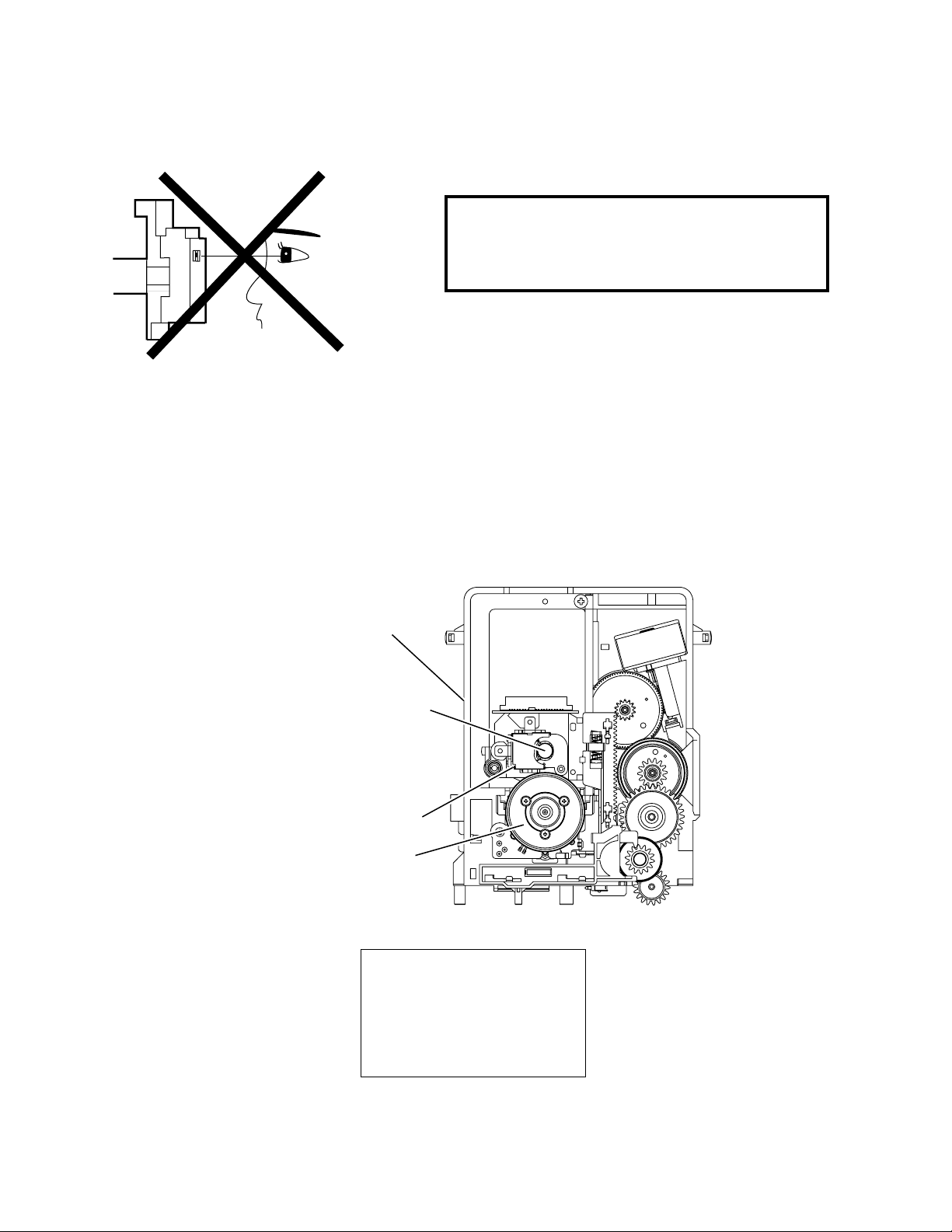
LASER BEAM SAFETY PRECAUTIONS
This DVD player uses a pickup that emits a laser beam.
Do not look directly at the l aser beam coming
from the pickup or allo w it t o str ike agai nst your
skin.
The laser beam is emitted from the locatio n shown in the figure. When ch ecking the laser d iode, be sure to keep
your eyes at least 30cm away from the pickup lens when the diode is tur ned on. Do not loo k directly at the laser
beam.
Caution: Use of controls an d adjustments, or doing pr ocedures other than th ose specified here in, may result in
hazardous radiation exposure.
Drive Mecha Assembly
Laser Beam Radiation
Laser Pickup
Turntable
WHEN OPEN. DO NOT
CAUTION
LASER RADIATION
STARE INTO BEAM.
Location: Inside Top of DVD mechanism.
1-2-1 DVD_LASER
Page 7

IMPORTANT SAFETY PRECAUTIONS
Product Safety Notice
Some electrical and mechanical parts have special
safety-related characteristics which are often not evident from visual inspection, nor can the protection they
give necessarily be obtained by replacing them with
components rated for higher voltage, wattage, etc.
Parts that have special safety characteristics are iden tified by a # on schematics and in parts lists. Use of a
substitute replacement that does not have the same
safety characteristics as the recommended replacement par t might create shock, fire, and/or other h azards. The Product’s Safety is under review
continuously and new instructions are issued whenever appropriate. Prior to shipment from the factory,
our products are carefully inspected to confirm with
the recognized product safety and electrical codes of
the countries in which they are to be sold. However, in
order to maintain such compli ance, it is equall y impor tant to implement the following precautions when a set
is being serviced.
Precautions during Servicing
A. Parts identified by the # symbol are critical for
safety. Replace only with part number specified.
B. In addition to safety, other parts and assemblies
are specified for conformance with regulations
applying to spurious radiation. These must also be
replaced only with specified re pla ce men ts.
Examples: RF converters, RF cables, noise blocking capacitors, and noise blocking filters, etc.
C. Use specified internal wiring. Note especially:
1)Wires covered with PVC tubing
2)Double insulated wires
3)High voltage leads
D. Use specified insulating materials for hazardous
live parts. Note especially:
1)Insulation tape
2)PVC tubing
3)Spacers
4)Insulators for transistors
E. When replacing AC primary side components
(transformers, power cord, etc.), wrap ends of
wires securely about the terminals before soldering.
F. Observe that the wires do not conta ct heat produc -
ing parts (heats inks, oxide metal fil m resis tors, fusible resistors, etc.).
G. Check that replaced wires do not contact sharp
edges or pointed parts.
H. When a power cord has been replaced, check that
5 - 6 kg of force in any direction will not loosen it.
I. Also check areas surrounding repair ed loc at ion s.
J. Be careful that foreign objects (screws, solder
droplets, etc.) do not remain inside the set.
K. Crimp type wire connector
The power transformer uses cri mp type con nector s
which connect the power cord and the primary side
of the transformer. When replacing the transformer,
follow these steps carefully and precisely to prevent
shock hazards.
Replacement procedure
1)Remove the old connector by cutting the wires at a
point close to the connector.
Important: Do not re-use a connector. (Discard it.)
2)Strip about 15 mm of the insulation from the ends
of the wires. If the wires are stranded, twist the
strands to avoid frayed conductors.
3)Align the lengths of the wires to be connected.
Insert the wires fully into the connector.
4)Use a crimping tool to crimp the metal sleeve at its
center. Be sure to crimp fully to t he complete closure of the tool.
L. When connecting or disconnecting the internal
connectors, first, disc onnect the AC plug from the
AC outlet.
1-3-1 DVD_SFN1
Page 8
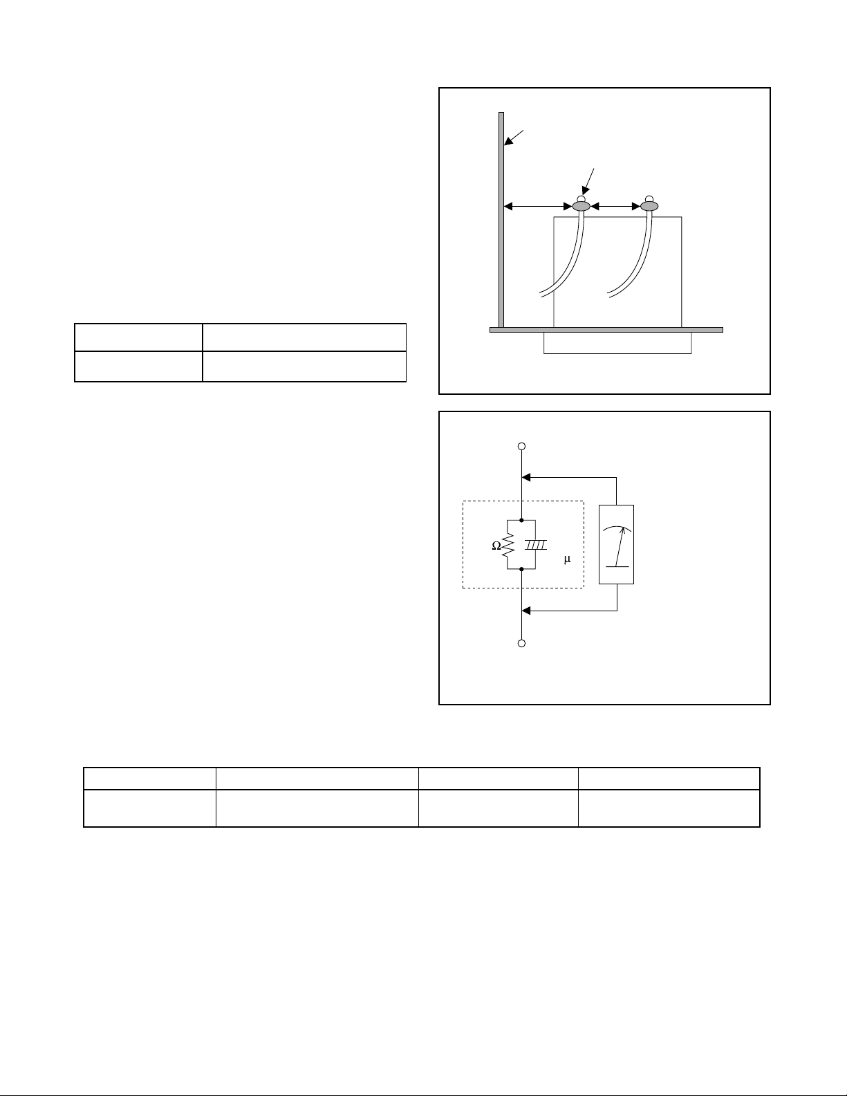
Safety Check afte r Servicing
Examine the area surrounding the repaired location for
damage or deteri oration. Observe that screws, par ts,
and wires have been returned to their original positions. Afterwards, do the following tests and confirm
the specified values to verify compliance with safety
standards.
1. Clearance Distance
When replacing primary circuit components, confirm
specified clearanc e distance (d ) and (d’) be tween soldered terminals, and between terminals and surrounding metallic parts. (See Fig. 1)
Table 1: Ratings for selected area
AC Line Voltage Clearance Distance (d) (d’)
Chassis or Secondary Conductor
Primary Circuit Terminals
dd'
120 V
Note: This table is unofficial and for reference only.
Be sure to confirm the precise values.
2. Leakage Current Test
Confirm the specified (or lower) leakage current
between B (earth ground, power cord plug prongs)
and externally exposed accessible parts (RF terminals, antenna terminals, video and audio input and
output terminals, microphone jacks, earphone jacks,
etc.) is lower than or equal to the specified value in the
table below.
Measuring Method (Power ON) :
Insert load Z between B (earth ground, power cord
plug prongs) and exposed accessible parts. Use an
AC voltmeter to measure across the ter minals of load
Z. See Fig. 2 and the following table.
Table 2: Leakage current ratings for selected areas
AC Line Voltage Load Z Leakage Current (i) Earth Ground (B) to:
120 V
≥ 3.2mm (0.126 inches)
0.15µF CAP. & 1.5kΩ RES.
Connected in parallel
Exposed Accessible Part
Z
1.5k
i≤0.5mA Peak Exposed accessible parts
0.15 F
Earth Ground
B
Power Cord Plug Prongs
AC Voltmeter
(High Impedance)
Fig. 1
Fig. 2
Note: This table is unofficial and for reference only. Be sure to confirm the precise values.
1-3-2 DVD_SFN1
Page 9
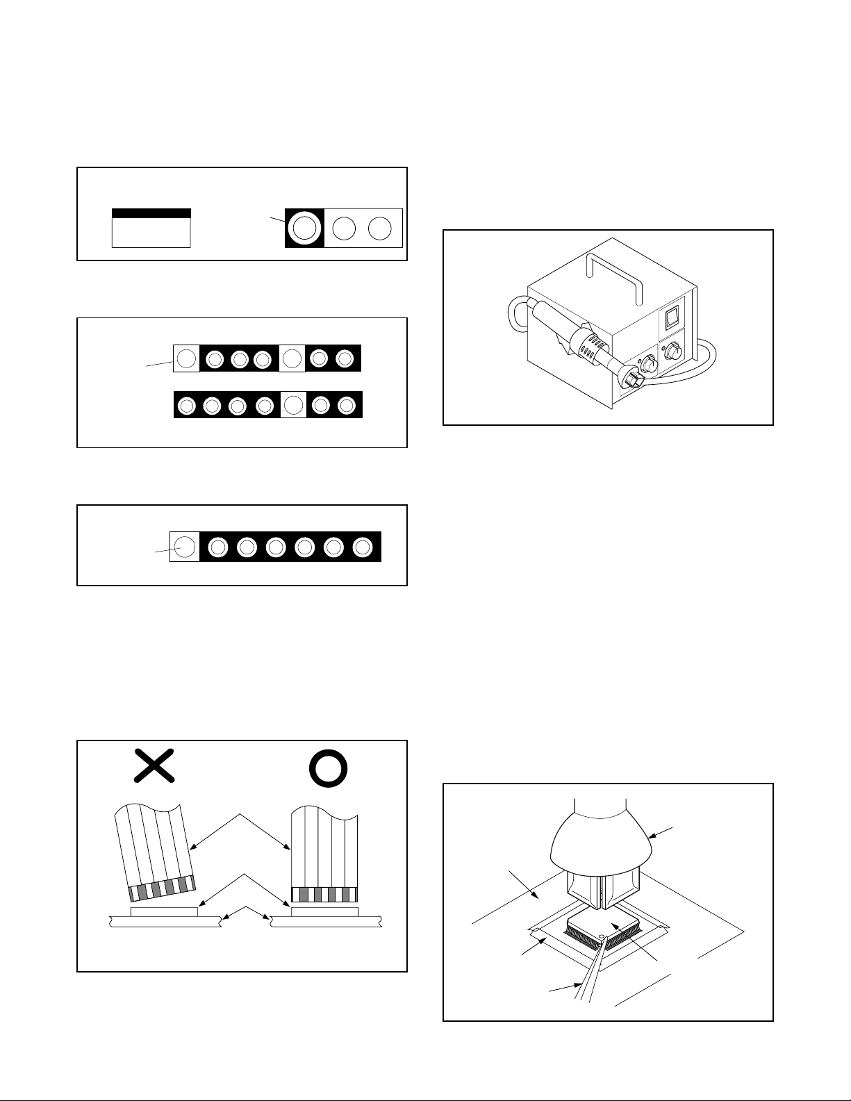
STANDARD NOTES FOR SERVICING
Circuit Board Indications
1. The output pin of the 3 pin Regulator ICs is indicated as shown.
Top View
Input
Out
2. For other ICs, pin 1 and every fifth pin are indicated
as shown.
In
Pin 1
3. The 1s t pin of every ma le c on nector i s indi ca ted a s
shown.
Pin 1
Bottom View
5
10
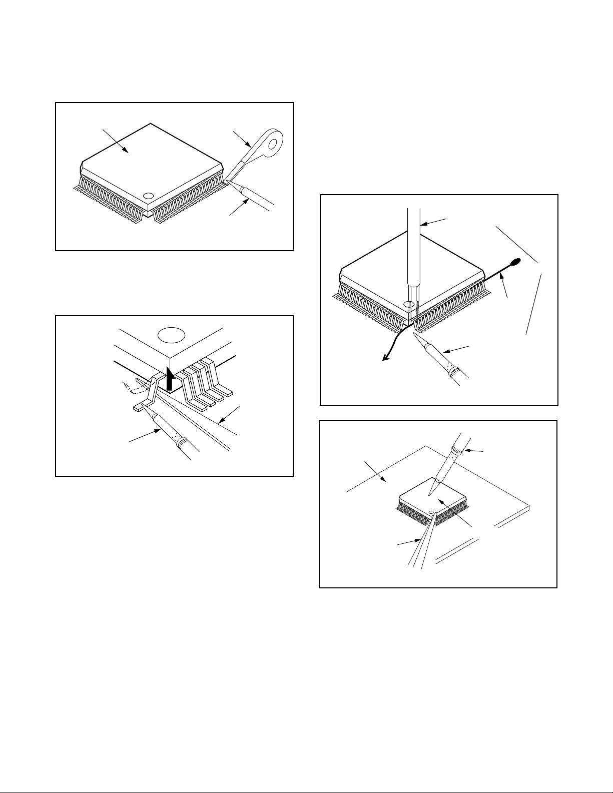
How to Remove / Install Flat Pack-IC
1. Removal
With Hot-Air Flat Pack-IC Desoldering Machine:.
(1) Prepare the hot-air flat pack-IC desoldering
machine, then apply hot air to the Flat Pack-IC
(about 5 to 6 seconds). (Fig. S-1-1)
Fig. S-1-1
(2) Remove the flat pack-IC with tweezers while apply-
ing the hot air.
(3) Bottom of the flat pack-IC is fixed with glue to the
CBA; when rem oving enti re flat pa ck-IC, first apply
soldering iron to ce nter of the flat pack-IC and hea t
up. Then remove (glue will be melted). (Fig. S-1-6)
(4) Release the flat pack-IC from the CB A using twee-
zers. (Fig. S-1-6)
Instructions for Connectors
1. When you conn ect or disconn ect t he FFC (Flexible
Foil Connector) cable, be sure to first disconnect
the AC cord.
2. FFC (Flexible Foil Connector) cable should be
inserted parallel into the connector, not at an angle.
FFC Cable
Connector
CBA
* Be careful to avoid a short circuit.
Caution:
1. D o not supply hot air to the chip par ts around the
flat pack-IC for over 6 seconds because damage to
the chip parts may occur. Put masking tape around
the flat pack-IC to protect other parts from damage.
(Fig. S-1-2)
2. The flat pack-IC on the CBA is affixed with glue, so
be careful not to brea k or damage the foil of each
pin or the solder lands under the IC when removing
it.
Hot-air
Flat Pack-IC
Desoldering
CBA
Masking
Tape
Tweezers
Machine
Flat Pack-IC
Fig. S-1-2
1-4-1 DVD_NOTE
Page 10
With Soldering Iron:
(1)Using desoldering braid, remove the solder from all
pins of the flat pack-IC. When you use solder flux
which is applied to all pins of the flat pack-IC, you
can remove it easily. (Fig. S-1-3)
Flat Pack-IC
Desoldering Braid
(4) Bottom of the flat pack-IC is fixed with glue to the
CBA; when rem oving enti re flat pa ck-IC, first apply
soldering iron to ce nter of the flat pack-IC and hea t
up. Then remove (glue will be melted). (Fig. S-1-6)
(5) Release the flat pack-IC from the CB A using twee-
zers. (Fig. S-1-6)
Note:
When using a solder ing iron, care must be taken
to ensure that the flat pack-IC is not bei ng held by
glue. When the flat pack-IC is removed from the
CBA, handle it gently beca use it may be damaged
if force is applied.
Soldering Iron
Fig. S-1-3
(2) Lift each lead of the flat pack-IC upward one by
one, using a shar p pin or wire to which s older will
not adhere (iron wi re). When he ating the pins, us e
a fine tip soldering iron or a hot air desoldering
machine. (Fig. S-1-4)
Sharp
Pin
Fine Tip
Soldering Iron
Fig. S-1-4
(3)Bottom of the flat pack-IC is fixed with glue to the
CBA; when removing entire flat pack-IC, first apply
soldering iron to c en ter of the flat pack-IC and heat
up. Then remove (glue will be melted). (Fig. S-1-6)
(4)Release the flat pa ck-IC from the CBA us ing twee-
zers. (Fig. S-1-6)
With Iron Wire:
(1)Using desoldering braid, remove the solder from all
pins of the flat pack-IC. When you use solder flux
which is applied to all pins of the flat pack-IC, you
can remove it easily. (Fig. S-1-3)
(2) Affix the wire to a workbench or solid mounting
point, as shown in Fig. S-1-5.
(3) While heating the pins using a fine tip soldering
iron or hot air blower, pull up the wire as the solde r
melts so as to lift the IC leads from the CBA contact
pads as shown in Fig. S-1-5
To Solid
Mounting Point
CBA
Tweezers
Hot Air Blower
or
Iron Wire
Soldering Iron
Fig. S-1-5
Fine Tip
Soldering Iron
Flat Pack-IC
Fig. S-1-6
1-4-2 DVD_NOTE
Page 11
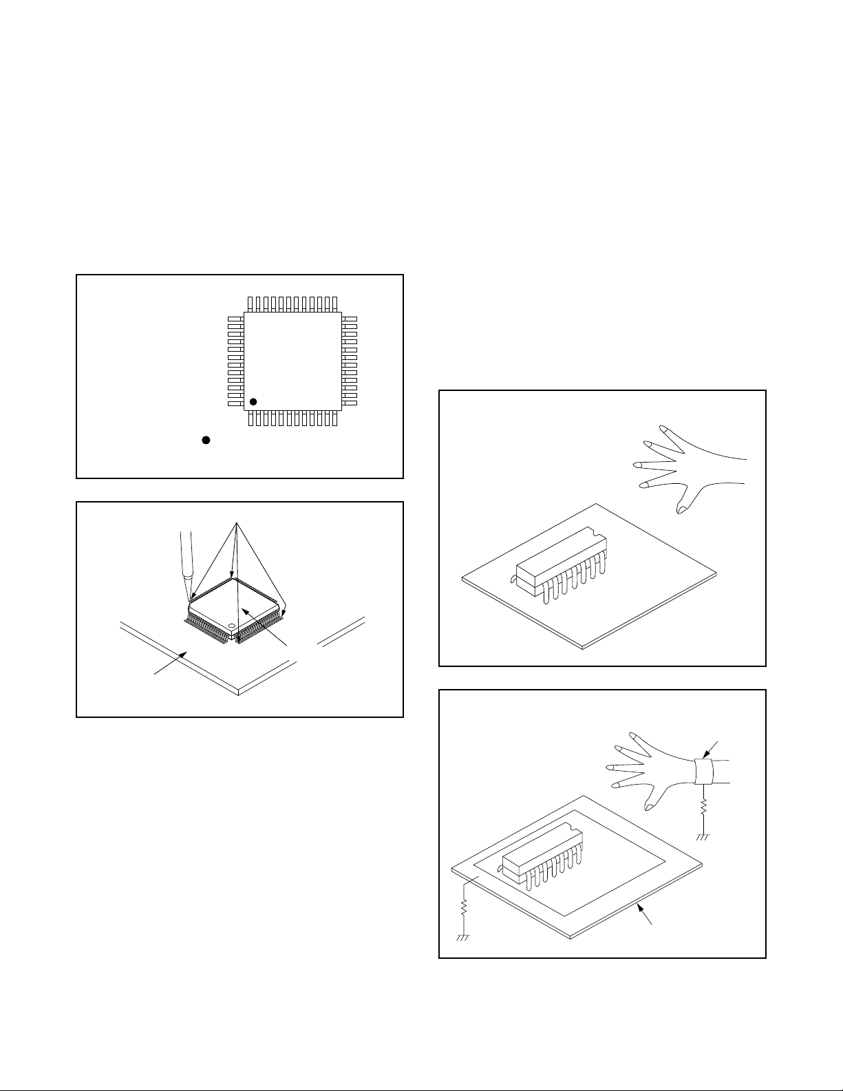
2. Installation
(1) Using desoldering braid, remove the solder from
the foil of each pin of the flat pack-IC on the CBA
so you can install a replacement fla t pack-IC more
easily.
(2) The “I” mark on the flat pack-IC indicates pin 1.
(See Fig. S-1-7.) Be s ure this mark matches the 1
on the PCB when positioni ng for installation. Then
presolder the four cor ners of the fl at pack-IC. (See
Fig. S-1-8.)
(3)Solder all pins of the flat pack-IC. Be sure that none
of the pins have solder bridges.
Example :
Pin 1 of the Flat Pack-IC
is indicated by a " " mark.
Fig. S-1-7
Instructions for Handling
Semi-conductors
Electrostatic breakdown of the semi-conductors may
occur due to a potential di fference caused by electrostatic charge during unpacking or repair work.
1. Ground for Human Body
Be sure to wear a groun ding band (1M Ω) that is properly grounded to re move any static electr ici ty that may
be charged on the body.
2. Ground for Workbench
(1) Be sure to place a conductive sheet or copper plate
with proper grounding (1MΩ) on the workbench or
other surface, where the semi-conductors are to be
placed. Because the static electricity charge on
clothing will not escape thr ough the body grounding band, be careful t o avoid contacting semi-conductors with your clothing.
< Incorrect >
CBA
Presolder
Flat Pack-IC
Fig. S-1-8
CBA
< Correct >
Grounding Band
1MΩ
CBA
1MΩ
Conductive Sheet or
Copper Plate
1-4-3 DVD_NOTE
Page 12
PREPARATION FOR SERVICING
How to Enter the Service Mode
About Optical Sensors
Caution:
An optical sensor system is used for the Tape Start
and End Sensors on this equipment. Carefully read
and follow the instructions below. Otherwise the unit
may operate erratically.
What to do for preparation
Insert a tap e into the Deck Mechan ism Assembly and
press the PLAY button. The tape will be loaded into
the Deck Mechanism Assembly. Make sure the power
is on, connect TP502 (SENSOR INHIBITION) to GND.
This will stop the functi on of Tape Star t Sensor, Tape
End Sensor and Reel Sensor s. (If these TPs are connected before plugging in the unit, the function of the
sensors will stay valid.) See Fig. 1.
Q503
Q504
TP502
S-INH
Fig. 1
Note: Because the Tape E nd Sensor s are in active, do
not run a tape all the way to the start or the en d of the
tape to avoid tape damage.
1-5-1 H9400PFS
Page 13
e
or
er
ut
e
ut
e
re
rd
d-
d
to
y
h
er
It
h
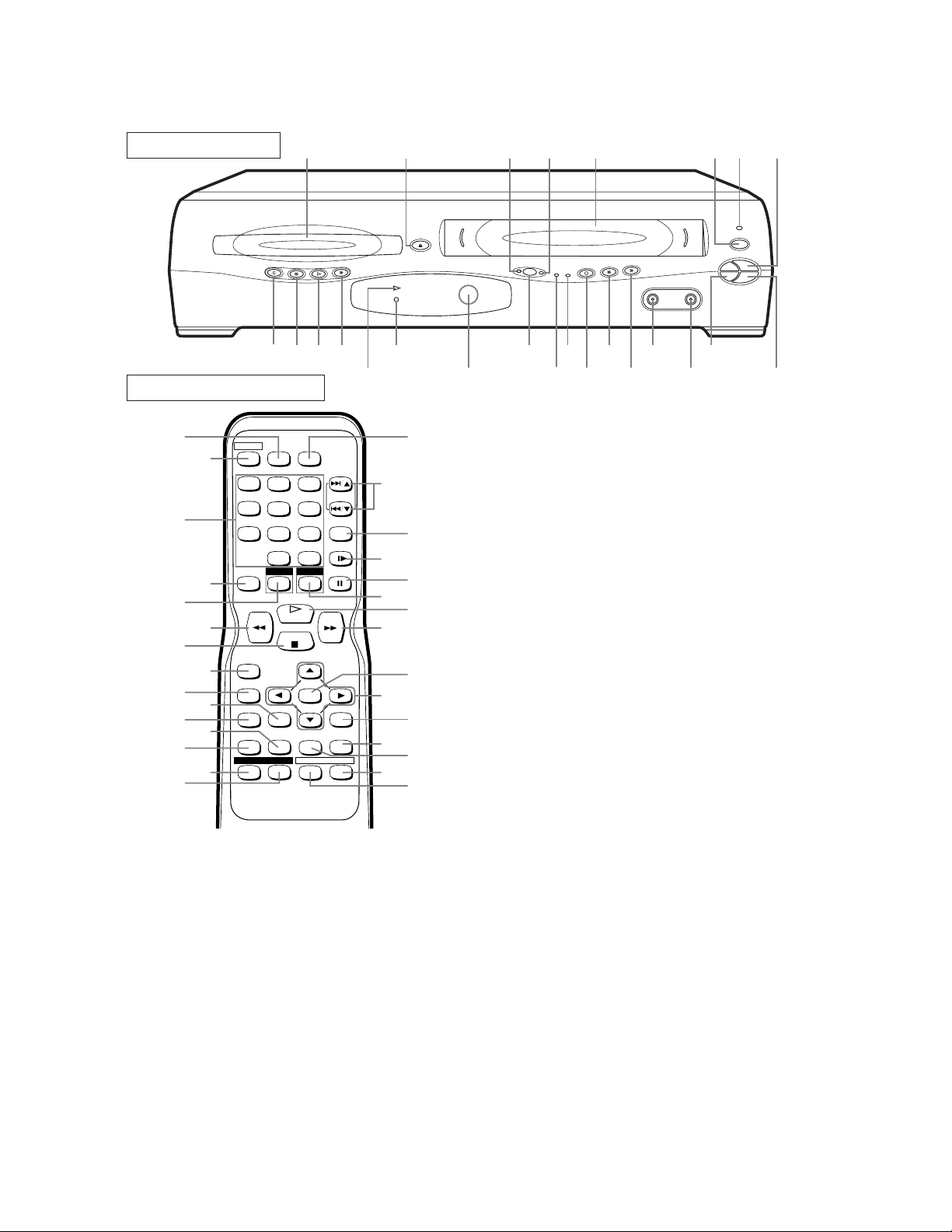
OPERATING CONTROLS AND FUNCTIONS
FRONT PANEL
1 2 3 4 768
OPEN/CLOSE
STOP
25
FWD
REV PLAY
2324 22 20
PLAY
DISC IN
REMOTE CONTROL
26
POWER
SPEED AUDIO
27
28
123
456
789
010
DVD VCR
DISPLAY
SKIP/CH.
VCR/TV
SLOW
+
PAUSE
29
30
31
32
34
33
35
RECORD
MENU
SETUP
36
37
38
39
40
1. Disc loading tray
2. OPEN/CLOSE Button
Press to insert discs into or remove them from the
tray.
3. DVD OUTPUT Light (Green)
This light appears when the DVD output mode is
selected. You can only watch DVDs when the green
DVD OUTPUT light is on. To make the green DVD
OUTPUT light come on, press DVD on the remote
control or OUTPUT on the front panel.
4. VCR OUTPUT Light (Green)
This light appears when the VCR output mode is
selected. You can only watch tapes when the green
VCR OUTPUT light is on. To make the green VCR
OUTPUT light come on, VCR on the remote control
or OUTPUT on the front panel.
5. CASSETTE COMPARTMENT
SUBTITLE
T-SET
ZOOMMODE
ANGLE
PLAY
STOP
ENTER
SEARCH
MODE
REPEAT
RETURNTITLE
CLEAR/
C.RESET
A-B
55
54
53
52
51
50
49
48
47
46
45
44
43
42
41
5
OUTPUT
DVD
VCR
TIMER REC
FF
REW
REC
18171615141312
19
6. POWER Button
Press to turn the power on and off.
7. POWER Light (red)
Light appears when the power is on.
8. STOP/EJECT Button (VCR)
EJECT Button
Press to remove the tape from the VCR.
STOP Button
Press to stop the tape motion.
9. PLAY Button(VCR)
Press to begin playback.
10. CH(ANNEL) Buttons
In VCR mode, press to change TV channels on th
VCR; press to adjust the tracking during normal
slow motion playback; press to remove vertical jitt
in a Still picture.
11. AUDIO In Jack
Connect an audio cable coming from the audio o
jack of a camcorder, another VCR, or an audio sourc
here.
12. VIDEO In Jack
Connect a video cable coming from the video o
jack of a camcorder, another VCR, or a video sourc
(laser disc player, camcorder, etc.) here.
13. FF Button (VCR)
Press to rapidly advance the tape, or view the pictu
rapidly in forward during playback. (Forwa
Search).
14. REW Button (VCR)
Press to rewind the tape, or to view the picture rapi
ly in reverse during the playback mode (Rewin
Search).
15. REC Button
Press once to start a recording. Press repeatedly
start a One-Touch Recording.
16. REC Light
Light appears during recording.
17. TIMER Light
Light appears when the DVD/VCR is in standb
mode for a timer recording or during a One-Touc
Recording. It flashes if T-SET is pressed for a tim
recording, but there is no tape in the DVD/VCR.
flashes when all timer recordings or One-Touc
Recordings are finished.
VIDEO AUDIO
11
POWER
CH-UP
STOP/EJECT
PLAY
CH-DOWN
10
921
1-6-1 H9411IB
Page 14

1
8. OUTPUT Button
1
2
2
2
2
2
2
2
2
2
2
3
3
k
l
r
e
r
,
c
.
e
-
r
o
.
k
t.
n
-
Press to select DVD mode or VCR mode.
●You can switch the output mode either by pressing
OUTPUT on the front panel, or by pressing DVD
or VCR on the remote control. However, if you
press OUTPUT on the front panel first, you
need to re-select the corresponding mode by
pressing DVD or VCR on the remote control.
9. Remote Sensor Window
0. DISC IN Light (green)
Light appears when a disc is in the DVD Player.
1. PLAY Light (green)
Light appears during Disc playback.
2. FWD Button (DVD)
Press to fast forward the Disc. Press PAUSE, then
press this button to begin slow motion playback.
Press this button repeatedly to change the forward
speed of slow motion.
Press to skip Chapters or Tracks.
3. PLAY Button (DVD)
Press to begin playback.
4. REV Button (DVD)
Press to view the DVD picture in fast reverse motion
or to reverse playback of an Audio CD.
Press to skip Chapters or Tracks.
5. STOP Button (DVD)
Stops operation of the disc.
6. SPEED Button
Press to select the VCR’s recording speed
(SP or SLP)
7. POWER Button
Press to turn the power on and off.
8. Number Buttons
●DVD mode
Press to select numbered items in a menu.
+10
Use this button to enter number 10 and above.
●VCR mode
Press to select TV channels on the VCR.
To select channels, enter channel numbers as a
two-digit number for the quickest results. For
example, to select channel 6, press 0 then 6.
9. DISPLAY Button
●DVD mode
Press to access or remove the display screen during
DVD or Audio CD playback.
●VCR mode
Press to access or remove the VCR’ s on-screen status display.
0. DVD Button
Press to select DVD mode for the remote control.
●You can switch the OUTPUT mode either by
pressing OUTPUT on the front panel, or by pressing
DVD or VCR on the remote control. However, if you
press OUTPUT on the front panel first, you need
to re-select the corresponding mode by pressing
DVD or VCR on the remote control.
1. h Button
●DVD mode
Press to view the DVD picture in fast reverse
motion.
slow motion playback. Press this button repeatedly to
change the reverse speed of slow motion.
●VCR mode
Press to rewind the tape, or to view the picture rapidly
in reverse during the playback mode (Rewind Search).
Press PAUSE, then press this button to begin
32. STOP Button
●DVD mode
Press to stop the disc motion.
●VCR mode
Press to stop the tape motion.
33. RECORD Button
Press once to start a recording.
34. MENU Button
●DVD mode
Press to display the menu of the Disc.
●VCR mode
Press to access the VCR menu.
35. TITLE Button
36. SETUP Button
Press to enter DVD player setup mode.
37. ZOOM Button
Enlarges part of a DVD-reproduced image.
38. MODE Button
Activates program playback or random playbac
mode when playing CDs or MP3. Sets Black leve
and virtual surround.
39. SUBTITLE Button
Press to select the desired subtitle language.
39. T-SET Button
Press to put the VCR into standby mode for a time
recording.
40. ANGLE Button
Press to change the camera angle to see the sequenc
being played back from a different angle.
41. REPEAT Button
Repeats playback of the current disc, title, chapter o
track.
42. A-B REPEAT Button
Repeats playback of a selected section.
43. SEARCH MODE Button
●DVD mode
Press to access or remove the Search display
which allows you to go directly to a specifi
Title/Chapter/Track/Time.
●VCR mode
Press to perform a Time Search or an Index Search
44. CLEAR/C.RESET Button
●DVD mode
Press to reset the setting.
●VCR mode
Press to reset the counter. Press to exit from th
MENU screen.
45. RETURN Button
●DVD mode
Returns to the previous operation.
46. Arrow Buttons
Use when making settings while watching the dis
play on a TV screen.
●DVD mode
Moves the cursor and determines its position.
●VCR mode
p/o Buttons
Press to enter digits when setting program (Fo
example: setting clock or timer program). Press t
select the setting modes from the on screen menu
B Button
When setting program (For example: setting cloc
or timer program), press to determine your selec
tion and proceed to the next step you want to inpu
Press to determine the setting modes from the o
screen menu. Press to add or delete channel num
bers during channel preset.
1-6-2 H9411IB
Page 15

s Button
4
4
4
5
to
e
e
e
h
to
e
in
k.
to
d-
d
R
n
aht
ts
re
e
Press to cancel a setting of timer program. Press to
correct digits when setting program (For example:
setting clock or timer program). Press to add or
delete channel numbers during channel preset.
7. ENTER Button
●DVD mode
Press to accept a setting.
8. g Button
●DVD mode
Press to fast forward the Disc. Press PAUSE, then
press this button to begin slow motion playback.
Press this button repeatedly to change the forward
speed of slow motion.
●VCR mode
Press to rapidly advance the tape, or view the picture rapidly in forward during playback (Forward
Search).
9. PLAY Button
●DVD mode
Press to begin playback.
●VCR mode
Press to begin playback.
0. VCR Button
Press to select VCR mode for the remote control.
●You can switch the OUTPUT mode either by
pressing OUTPUT on the front panel, or by pressing
DVD or VCR on the remote control. However, if you
press OUTPUT on the front panel first, you need
to re-select the corresponding mode by pressing
DVD or VCR on the remote control.
51. PAUSE Button
●DVD mode
Press to pause Disc playback. Press repeatedly
advance the DVD picture step by step (or on
frame at a time).
●VCR mode
While recording, press to temporarily stop th
recording (pause). Press a second time to resum
normal recording. You can not pause a One-Touc
Recording. Or, press during tape playback
freeze the picture. Press to advance the picture on
frame at a time during still mode.
52. SLOW Button
During tape playback, press to view the video tape
slow motion. Press again to resume normal playbac
This button does not affect DVD playback.
53. VCR/TV Button
Use to select VCR or TV position.
●VCR Position
To view playback, to monitor video recording or
watch TV using the VCR tuner.
●TV Position
To watch TVor to view one program while recor
ing another.
54. SKIP/CH. Buttons
●DVD mode
Press to skip Chapters or Tracks.
●VCR mode
Press to change TV channels on the VCR.
55. AUDIO Button
Press to select a desired audio language or soun
mode.
Notes
To use the remote control to operate the DVD/VC
COMBINATION UNIT and its features, press DVD o
the remote control before pressing other DVD oper
tion button. Verify that the green DVD OUTPUT Lig
is on.
To use the remote control to operate the VCR and i
features, press VCR on the remote control befo
pressing other VCR operation button. Verify that th
green VCR OUTPUT Light is on.
1-6-3 H9411IB
Page 16
1
2
3
N
5
5
5
5
6
6
e
p-
S-
a
e
d
is
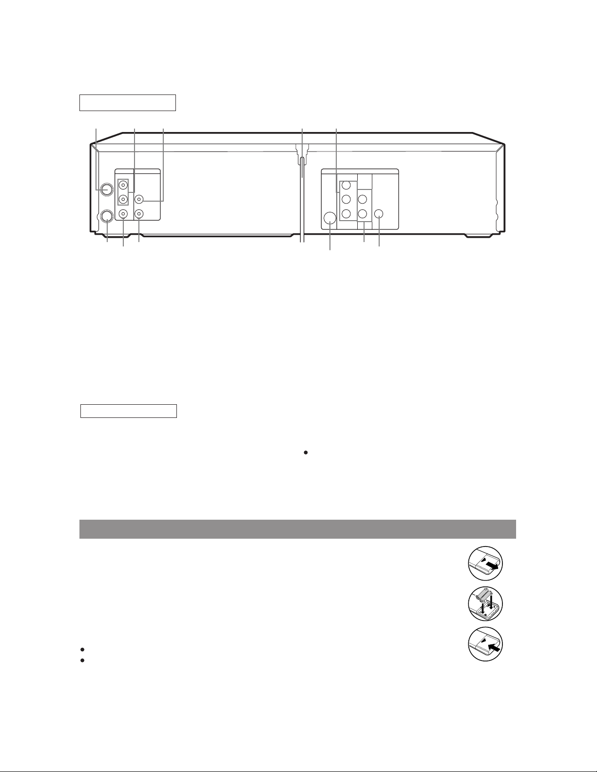
REAR VIEW
5756 58 59 60
DVD/VCR VCR DVD
AUDIO OUT
ANT-IN
L
AUDIO IN
R
ANT-OUT
VIDEO OUT
VIDEO IN
S-VIDEO
OUT
COMPONENT
VIDEO OUT
Y
CbCrL
AUDIO
OUT
R
COAXIAL
DIGITAL
AUDIO OUT
66
6. ANT-IN (Antenna In) Jack
Connect your antenna, Cable Box, or Satellite decoder
box.
7. DVD/VCR AUDIO OUT Jacks
Connect the supplied audio cables here and to the
Audio In jacks of a television or other audio equipment.
8. AUDIO IN Jack
Connect an audio cable coming from the audio out
jack of a camcorder, another VCR, or an audio
source here.
9. AC Power Cord
Connect to a standard AC outlet to supply power to
the DVD/VCR COMBINATION UNIT.
DVD Playback only
0. COMPONENT VIDEO OUT Jacks
Connect optional component video cables here and
to the component Video In jacks of a television.
1. COAXIAL Jack
Connect an optional coaxial digital audio cable here
and to the Coaxial Digital Audio In jack of a decoder
or audio receiver.
65
64
63
62. DVD ANALOG AUDIO OUT Jacks
Connect the supplied audio cables here and to th
Audio In jacks of a television or other audio equi
ment (DVD only).
63. S-VIDEO OUT Jack
Connect an optional S-Video cable here and to the
Video In jack of a television. (DVD only).
64. VIDEO IN Jack
Connect a cable coming from the video out jack of
camcorder, another VCR, or an audio-visual sourc
(laser disc player, video disc player, etc.) here.
65. DVD/VCR VIDEO OUT Jack
Connect the yellow video cable (supplied) here an
to the TV’s Video In jack.
66. ANT-OUT (Antenna Out) Jack
Use the supplied RF coaxial cable to connect th
jack to the ANTENNAIN Jack on your TV.
Notes
The S-VIDEO OUT jack, COAXIAL jack, and COM
PONENT VIDEO OUT jack are only useful in DVD
mode.
Caution: Do not touch the inner pins of the jacks
on the rear panel. Electrostatic discharge may
62
61
cause permanent damage to the player.
LOADING THE BATTERIES
. Open the battery compartment cover.
. Insert two AA batteries (supplied), with each one oriented correctly.
. Close the cover.
otes
Do not mix alkaline and manganese batteries.
Do not mix old and new batteries.
1-6-4 H9411IB
Page 17
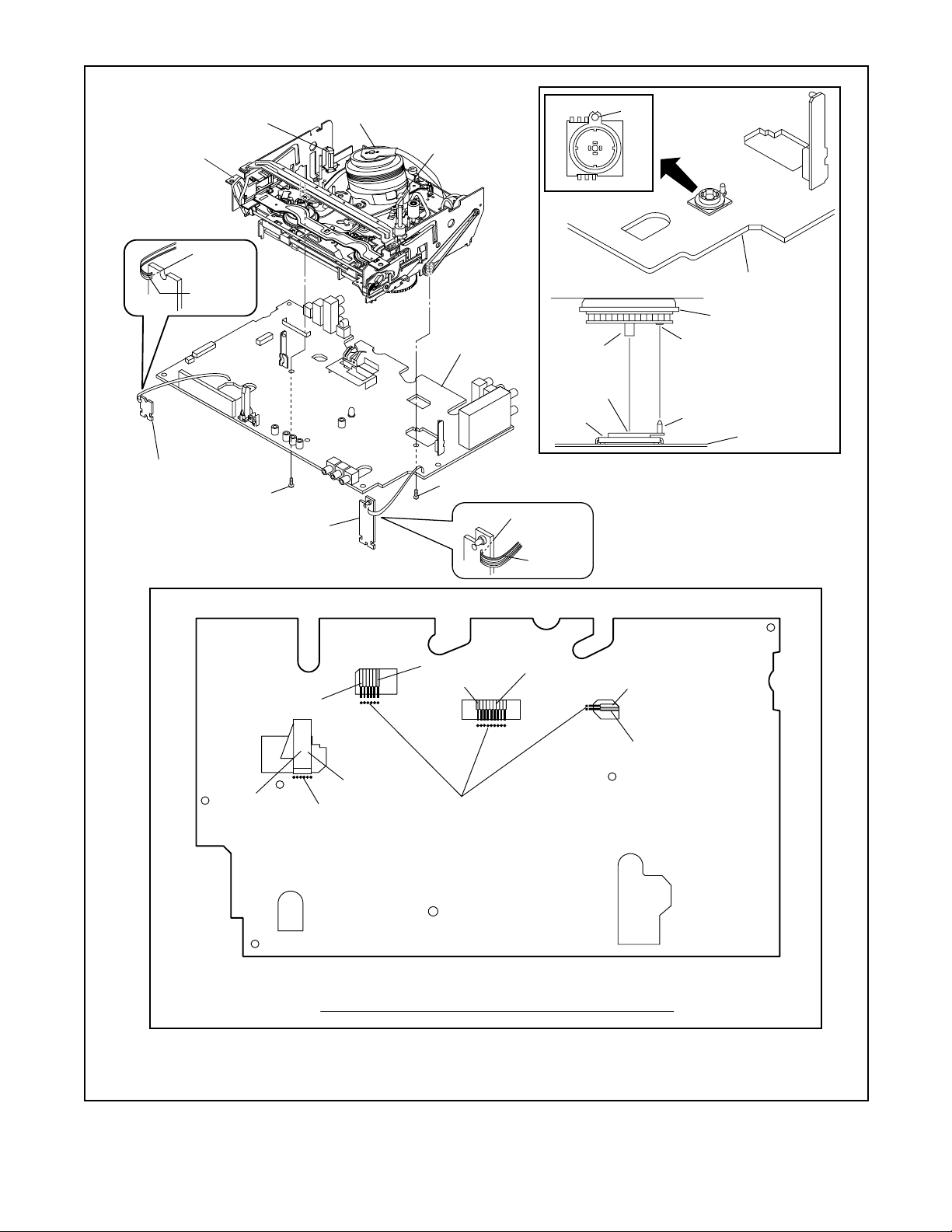
CABINET DISASSEMBLY INSTRUCTIONS
1. Disassembly Flowchart
This flowchart indicates the disassembly steps to gain
access to item(s) to be ser vic ed. When reasse mbling,
follow the steps in reverse order. Bend, route, and
dress the cables as they were originally.
[1] Top Cover
[2] Front
Assembly
[16] Side
Bracket
[5] DVD Main
CBA Unit
[13] DVD OP/CL
CBA
[12] Main CBA
[3] Top Bracket
[4] DVD Mecha
Assembly
[6] Rear Unit
[10] VCR
Chassis Unit
[9] Rear Panel
[8] PCB Bracket
[7] Power
Supply CBA
[11] Deck
Assembly
REMOVAL
ID/
LOC.
No.
[7]
[8]
[9]
[10]
[11]
[12] Ma in CBA D8 ---------- -
[13]
PART
Power Supply CBA
PCB
Bracket
Rear Panel
VCR
Chassis
Unit
Deck
Assembly
Open/
Close
CBA
REMOVE/*UNHOOK/
Fig.
UNLOCK/RELEASE/
No.
UNPLUG/DESOLDER
D6 4(S-8) -
D6 3(S-9) -
D6 ---------- -
D7 5(S-10), 4(S-11) -
D8 Desolder, 2(S-12) 4,5
D8 ---------- -
Note
[14] Function
CBA
[15] Deck
Pedestal
2. Disassembly Method
REMOVAL
ID/
LOC.
No.
[1] Top Cover D1 7(S-1) -
[2]
[3]
[4]
[5]
PART
Front
Assembly
Top
Bracket
DVD
Mecha
Assembly
DVD Main
CBA Unit
REMOVE/*UNHOOK/
Fig.
UNLOCK/RELEASE/
No.
UNPLUG/DESOLDER
D2 (S-3), *7(L-1)
D2 4(S-2) -
3(S-4), *CN401,
D3
*CN601,*CN302
2(S-5), *CN201,
D4
*CN301
Note
1
1-1
1-2
-
2
2-1
2-2
3
[14]
[15]
[16]
Note:
(1): Identification (location) No. of parts in the figures
(2):Name of the part
(3):Figure Number for reference
(4): Identification of parts to be removed, unhooked,
(5): Refer to “Reference Notes.”
Function
CBA
Deck
Pedestal
Side
Bracket
↓
(1)
unlocked, released, unplugged, unclamped, or
desoldered.
P=Spring, L=Locking Tab, S=Screw,
CN=Connector
*=Unhook, Unlock, Release, Unplug, or Desolder
e.g. 2(S-2) = two Screws (S-2),
2(L-2) = two Locking Tabs (L-2)
↓
(2)
D8 ---------- -
D9 7(S-13) -
D9 (S-14) -
↓
(3)
↓
(4)
↓
(5)
[6] Rear Unit D5
5(S-6), 3(S-7),
CN1005
-
1-7-1 H9411DC
Page 18
Reference Notes
CAUTION 1: Locking Tabs (L-1) are fragil e. Be caref ul
not to break them.
1-1. Remove Screw (S-3).
1-2. Release seven Locking Tabs (L-1) (to do this, first
release five Locking Tabs (A) at th e side and top,
and then release two Locking Tabs (B) at the bottom.)
CAUTION 2: Electrostatic breakdown of the laser
diode in the optical system block may occur as a
potential difference caused by electrostatic charge
accumulated on cloth, human body etc., during
unpacking or repair work.
To avoid damage of pickup follow next procedures.
2-1. Short the three short lands of FPC cable with sol-
der before removing the FFC cable (CN201) from
it. If you disconnect the FFC ca ble (CN201), the
laser diode of pickup will be destroyed. (Fig. D4)
2-2. Disconnect Connector (CN301). Remove two
Screws (S-5) and lift the DVD Main CBA Unit.
(Fig. D4)
CAUTION 3: When reassembling, confirm the FFC
cable (CN201) is conne cted compl etely. Then remove
the solder from the three short lands of FPC cable.
(Fig. D4)
4. When re ass em bling, s old er wire j ump er s a s s hown
in Fig. D8.
5. Before installing the Deck Assembly, be sure to
place the pin of LD-SW on M ain CBA as shown in
Fig. D8. Then, install the Deck Assembly while
aligning the hole of Cam Gear with the pin of LDSW, the shaft of Cam Gear with the hole of LD -S W
as shown in Fig. D8.
(L-1)
(A)
(L-1)
(S-3)
(B)
[2] Front Assembly
CN601
CN302
(S-4)
CN401
(S-2)
(S-2)
[3] T op Bracket
(S-2)
(A)
(L-1)
(A)
Fig. D2
(S-4)
(S-4)
[4] DVD Mecha Assembly
(S-1)
[1] T op Cover
(S-1)
Fig. D1
Fig. D3
(S-1)
1-7-2 H9411DC
Page 19
(S-5)
CN301
CN201
(S-5)
[5] DVD Main
CBA Unit
A
DVD Mecha
[6] Rear Unit
(S-7)
(S-6)
(S-7)
(S-6)
CN1005
(S-7)
B
Short the three short lands by soldering
Connector
View for A
OR
Slide
C
Pickup Unit
Short the three short
lands by soldering
View for B
FPC Cable
View for C
Fig. D4
(S-8)
(S-8)
(S-11)
[10] VCR Chassis Unit
[8] PCB Bracket
[7] Power Supply CBA
(S-11)
(S-10)
Fig. D5
(S-9)
[9] Rear Panel
Fig. D6
(S-10)
(S-11)
(S-10)
(S-11)
Fig. D7
1-7-3 H9411DC
Page 20
FE Head
[11] Deck
Assembly
Desolder
Lead with
blue stripe
[13] DVD OP/CL CBA
(S-12)
[14] Function CBA
Cylinder Assembly
AC Head
Assembly
[12] Main CBA
(S-12)
Desolder
[11] Deck Assembly
Shaft
LD-SW
Lead with
blue stripe
Pin
SW507
LD-SW
[12] Main CBA
Cam Gear
Hole
Hole
Pin
[12] Main CBA
From
AC Head
Assembly
From
Capstan
Motor
Assembly
From
Cylinder
Assembly
Printing side
Desolder
Lead with
blue stripe
Desolder
BOTT OM VIEW
Lead connections of Deck Assembly and Main CBA
From
FE Head
Lead with
white stripe
Fig. D8
1-7-4 H9411DC
Page 21
[15] Deck Pedestal
(S-13)
(S-14)
[16] Side
Bracket
(S-13)
HOW TO MANUAL EJECT
Fig. D9
1. Remove the Top Case.
2. Rotate this roulette in the direction of the arrow as
shown below.
Top Cover
1
DVD Mecha
Tray
Deck Assembly
3
2
Rotate this roulette in
the direction of the arrow
2
1-7-5 H9411DC
Page 22
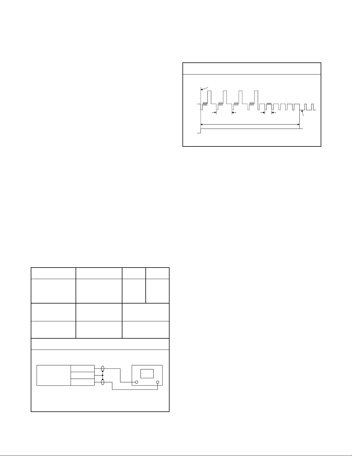
ELECTRICAL ADJUSTMENT INSTRUCTIONS
General Note: "CBA" is an abbreviation for
"Circuit Board Assembly."
NOTE:
1.Electric al adjust ments are required a fter repla cing
circuit components and certain mechanical parts. It
is importan t to do these adjustments onl y after all
repairs and replacements have been completed.
Also, do not attempt these adjus tments u nle ss the
proper equipment is available.
2.To perform th ese alignment / confirmation proce dures, make sure that the tracking control is set in
the center position: P ress ei ther "CHA NNEL L5 ??" or
"CHANNEL K" button on th e front panel first , then
the "PLAY" button on the front panel.
CH1
CH2
Figure 1
EXT. Syncronize Trigger Point
1.0H
6.5H±1H (412.7µs±60µs)
Switching Pulse
0.5H
V-Sync
Test Equipment Required
1.Oscilloscope: Dual-trace with 10:1 probe,
V-Range: 0.001~50V/Div.,
F-Range: DC~AC-20MHz
2.Alignment Tape (FL8A)
Head Switching Po sition Adjustment
Purpose:
To determine the Head Switching point during
playback.
Symptom of Mi sadjustm e n t:
May cause Head Switching noise or ver tical jitter
in the picture.
Test point Adj.Point Mode Input
TP751(V-OUT)
TP302(RF-SW)
GND
Tape
VR501
(Switching Point)
(MAIN CBA)
Measurement
Equipment
PLAY
(SP)
Spec.
Reference Notes:
Playback the Alignment tape and adjust VR501 so that
the V-sync front edge of the CH1 video output waveform is at the 6.5H(412 .7µs) del ayed position from the
rising edge of the CH2 head switching pulse waveform.
-----
FL8A Oscilloscope
Connections of Measurement Equipment
TP751
Main CBA
GND
TP302
6.5H±1H
(412.7µs±60µs)
Oscilloscope
CH1 CH2
Trig. (+)
1-8-1 H9400EA
Page 23
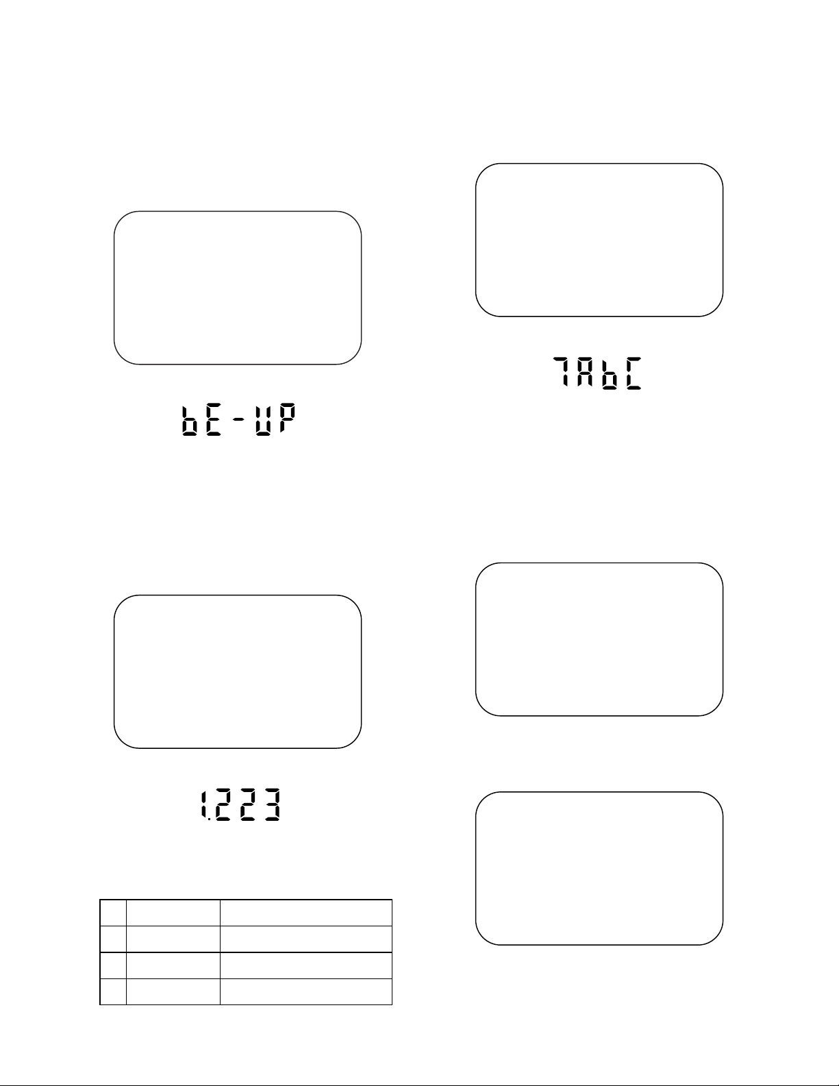
FIRMWARE RENEWAL MODE
1. Turn the power on and remove the disc on the tray.
2. To put the DVD player into version up mode, press
[9], [8], [7], [6], and [SEARCH MO DE] but tons on
the remote control unit in that order. The tray will
open automatically.
Fig. a appears on the screen and Fig. b appears on
the VFD.
F/W Version Up Mode
Please insert a DISC
for F/W Version Up.
EXIT: POWER
Fig. a Version Up Mode Screen
Fig. b VFD in Version Up Mode
The DVD player can also enter the version up
mode with the tray open. In this case, Fig. a will be
shown on the screen while the tray is open.
3. Load the disc for version up.
4. The DVD player enters the F/W version up mode
automatically. Fig. c appears on the screen and
Fig. d appears on the VFD.
F/W Version Up Mode
VERSION : ********
Reading...(*2)
5. A fter programming is fini shed, the tray opens au tomatically. Fig. e appears on the screen and the
checksum in (*3) of Fig. e appears on the VFD.
(Fig. f)
F/W Version Up Mode
VERSION : ********
Completed
SUM : 7abc (*3)
Fig. e Completed Program Mode Screen
Fig. f VFD upon Finishing the Programming Mode (Example)
At this time, no buttons are available.
6. Unplug the AC cord from the AC outlet. Then plug it
again.
7. Turn the power on by pressing the power button
and the tray will close.
8. Press [1], [2], [3], [4], and [DISPLAY] buttons on the
remote control unit in that order.
Fig. g appears on the screen.
model: ****** Ver: **** Region: **
1: VFD TEST
2: TT REPEAT PLAY
3: EEPROM CLEAR
4: MEASUREMENT SERVO
5: DISC READ CHECK
6: MECHA CHECK
7: DISC INFO
8: ERROR RATE
EXIT: POWERRETURN: -----
EXIT: POWER
Fig. c Programming Mode Screen
Fig. d VFD in Programming Mode (Example)
The appearance shown in (*2) of Fig. c is
described as follows:
AppearanceNo. State
Reading... Sending files into the memory
1
Erasing... Erasing previous version data
2
Programming...
3 Writing new version data
Fig. g
9. Press [3] button on the remote control unit.
Fig. h appears on the screen.
model: ****** Ver: **** Region: **
TEST 3: EEPROM CLEAR
EEPROM CLEAR: OK
EXIT: POWERRETURN: -----
Fig. h
10.To finish this mode, press [POWER] button.
1-9-1 H9400TEST
Page 24
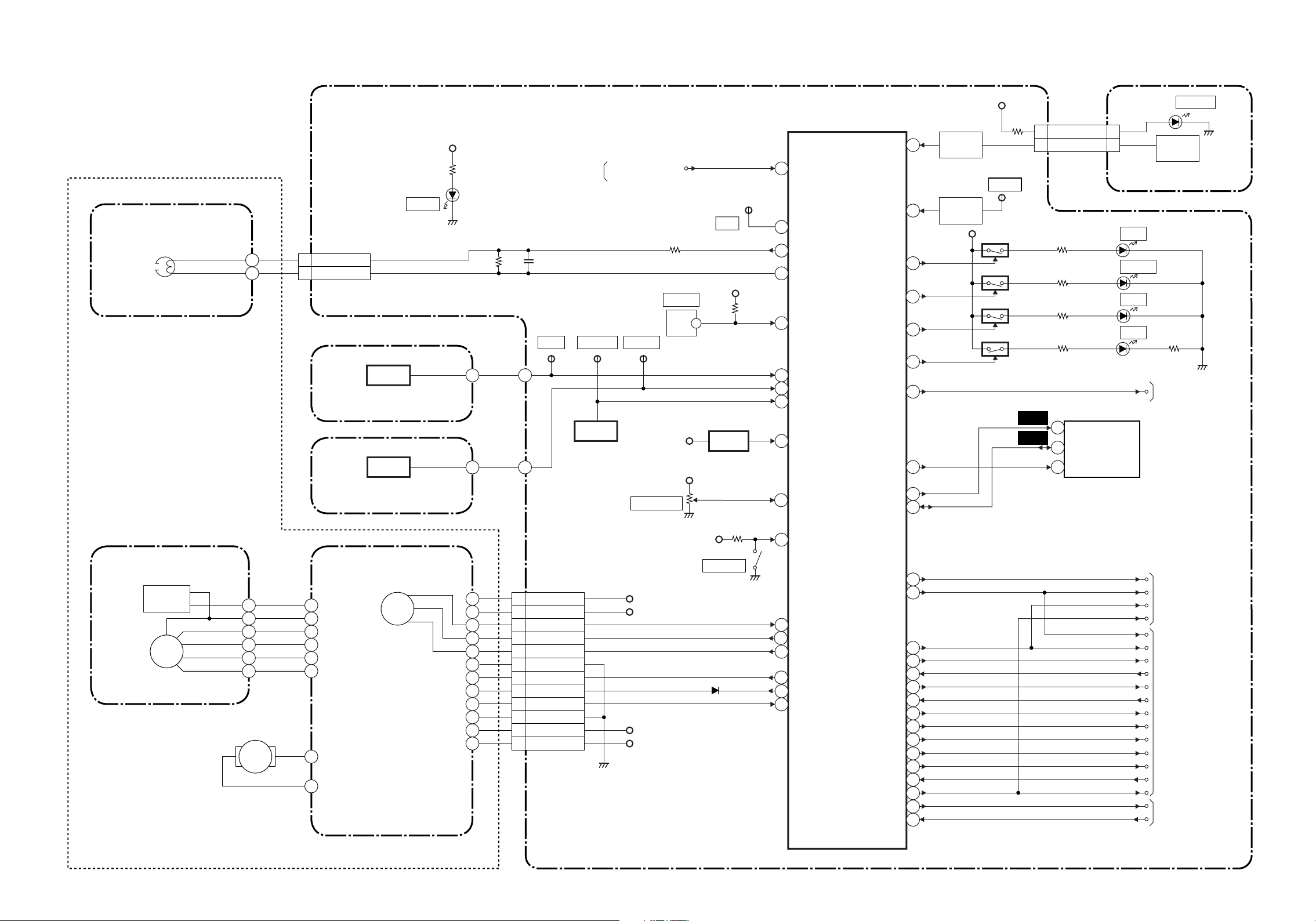
Servo/System Control Block Diagram
(DECK ASSEMBLY)
AC HEAD ASSEMBLY
CN504
CONTROL
HEAD
CL504
5 CTL(+)
6 CTL(-)
MAIN CBA
D555
S-LED
AL+5V
BLOCK DIAGRAMS <VCR SECTION>
IC501
(SERVO/SYSTEM CONTROL)
FROM/TO DVD SYSTEM
CONTROL BLOCK
DIAGRAM
<DVD SECTION>
REMOTE-VIDEO
SW512
LD-SW
TP513
CTL
AL+5V
REMOTE-VIDEO
5
58
CTL
56
CTL(+)
57
CTL(-)
KEY- 1
67
KEY- 2
66
REC-IND
TIMER-IND 75
72
P-ON+9V
KEY
SWITCH
KEY
SWITCH
TP502
S-INH
AL+5V
1 1POWER-LED
2 2KEY-1
Q565
Q563
CL508CL509
FUNCTION CBA
D565
REC
D564 TIMER
D566 VCR
D561
KEY
SWITCH
POWER
CYLINDER ASSEMBLY
PG
SENSOR
DRUM
MOTOR
M
LOADING
MOTOR
M
Q504
ST-S
SENSOR CBA
Q503
END-S
SENSOR CBA
CAPSTAN MOTOR
CAPSTAN
MOTOR
M
TP506
ST-S
CL502
1 AL+12V
2 P-ON+5V
3 C-FG
C-F/R
4
C-CONT
5
GND
6
LM-FWD/REV
7
D-CONT
8
D-PFG
9
GND
10
AL+12V
11
AL+15V
12
TP505
T-REEL
Q506
T-REEL
TP507
END-S
TIMER+5V
VR501
SW-POINT
AL+12V
P-ON+5V
AL+12V
AL+15V
AL+5V
AL+5V
Q501
RESET
SW511
REC SW
LD-SW68
69
ST-S
62
END-S
T-REEL
3
RESET
20
PG-DELAY
65
REC-
2
SAF-SW
49
C-FG
C-F/R
27
C-CONT
28
LM-FWD/REV
21
D-CONT29
D-PFG
47
VCR-IND 70
DVD-IND 71
DVD-POWER
VCR/TV
IIC-BUS SDA
A-MUTE-H
D-REC-H
D-PB-L
INSEL/ST-SL
C-SYNC
D-V SYNC
V-ENV
C-ROTA
RF-SW
TRICK-H
H-A-SW
H-A-COMP
OUTPUT-SELECT
P-ON-L
P-DOWN-L
26
77
13IIC-BUS SCL
12
24
23
16
41
19
64
78
18
11
14SP/LP/SLP
79
80
46
22
Q566
Q567
WF12
11
WF13
12
7
OUTPUT-SELECT
OUTPUT-SELECT
1
D567 DVD
DVD POWER
TU701(TUNER UNIT)
CLOCK
DATA
VCR/TV5
A-MUTE-H
D-REC-H
D-PB-L
D-REC-H
D-PB-L
INSEL/ST-SL
C-SYNC
D-V SYNC
V-ENV
C-ROTA
RF-SW
TRICK-H
SP/LP/SLP
H-A-SW
H-A-COMP
P-ON-L
P-DOWN-L
TO DVD SYSTEM
CONTROL BLOCK
DIAGRAM
<DVD SECTION>
TO AUDIO
BLOCK
FROM/TO
VIDEO BLOCK
FROM/TO POWER
SUPPLY BLOCK
1-10-1 1-10-2 H9411BLS
Page 25
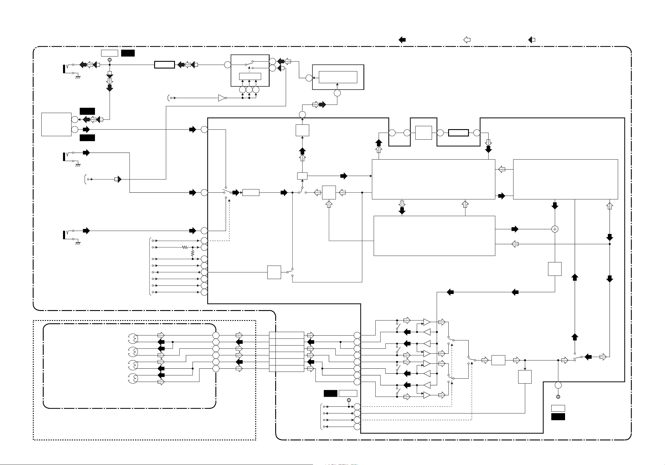
Video Block Diagram
TP751
V-OUT
JK751
V-OUT
TU701
VIDEO IN
VIDEO OUT
JK752
REAR
V-IN
WF11
6
18
WF15
WF1
FROM
SERVO/SYSTEM
CONTROL BLOCK
DIAGRAM
Q391
BUFFER
OUTPUT SELECT
IC301
42
15
Q760
(Y/C PROCESS)
TUNER
(OUTPUT SELECT)
IC751
SW CTL
9 10 11
VCR
DVD
REC VIDEO SIGNAL PB VIDEO SIGNAL DVD VIDEO SIGNAL MODE: SP/REC
1
IC501
(OSD)
MAIN CBA
2
OSD CHARACTER
38
MIX
40
35
6dB
AMP
45 47 49 44
CCD 1H
DELAY
Q301
BUFFER
FROM DVD
VIDEO/AUDIO
BLOCK DIAGRAM
<DVD SECTION>
JK753
FRONT
V-IN
(DECK ASSEMBLY)
DVD-VIDEO
FROM/TO
SERVO/SYSTEM
CONTROL BLOCK
DIAGRAM
VIDEO (R)-1 HEAD
VIDEO (L)-1 HEAD
VIDEO (L)-2 HEAD
VIDEO (R)-2 HEAD
CYLINDER ASSEMBLY
INSEL/ST-SL
D-PB-L
D-REC-H
TRICK-H
C-SYNC
C-ROTA
D-V SYNC
SP/LP/SLP
REAR
38
FRONT
40
71
16
REC/EE/PB
D-REC-H
11
TRICK
73
34
C-ROTA
14
D-V SYNC
39
SP/LP/SLP
59
V-AGC
SYNC
SEPA
R
P
CL253
V(R)-1
1
V-COM
2
V(L)-1
3
V(L)-2
4
V-COM
5
V(R)-2
6
FROM/TO
SERVO/SYSTEM
CONTROL BLOCK
DIAGRAM
FBC
R P
Y/C
MIX
TP302
RF-SW
WF2
RF-SW
V-ENV
H-A-SW
H-A-COMP
91
90
89
88
85
84
83
82
13
93
15
H-A-COMP
94
DOC YNR Y/C COMB
CHROMINANCE
SIGNAL PROCESS
R
L
L
R
SP
LP/EP
HPF
LUMINANCE
SIGNAL PROCESS
AGC
AMP
R
P
ENV
DET
74
TP301
C-PB
WF3
1-10-3 1-10-4 H9411BLV
Page 26
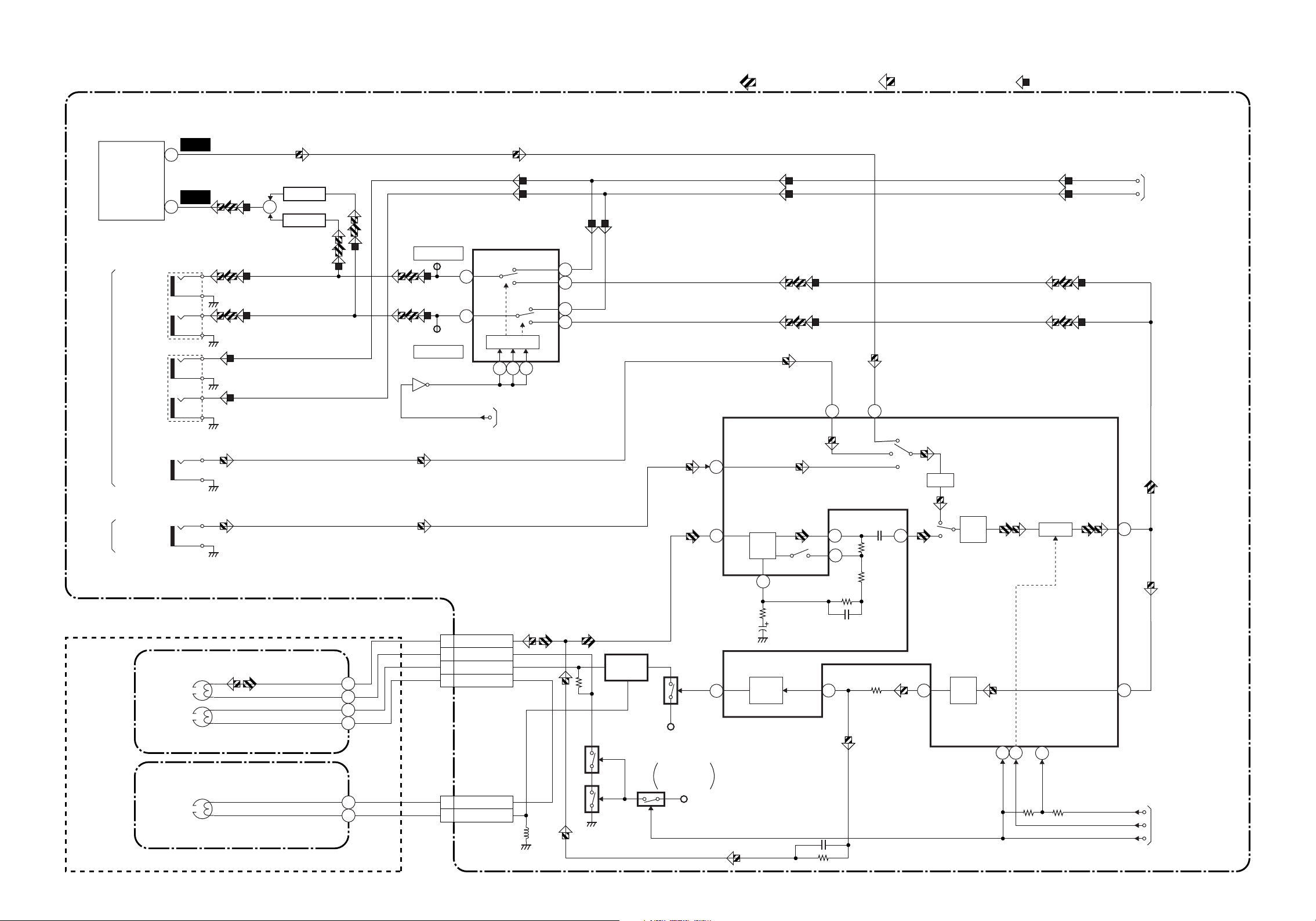
Audio Block Diagram
REAR
TU701
AUDIO-OUT
MOD-A
A-OUT (R)
A-OUT (L)
A-OUT (R)
A-OUT (L)
JK752
A-IN
14
2
JK751
JK756
WF14
WF10
+
Q763
BUFFER
Q762
BUFFER
TP753
A-OUT (R)
4
14
TP754
A-OUT (L)
Q760
OUTPUT SELECT
IC751
(OUTPUT SELECT)
DVD
VCR
DVD
VCR
SW CTL
9 10 11
FROM SERVO/SYSTEM
CONTOL BLOCK
DIAGRAM
12
13
PB-AUDIO SIGNAL REC-AUDIO SIGNAL Mode : SP/REC
DVD AUDIO SIGNAL
MAIN CBA
DVD-A(R)
DVD-A(L)
5
3
IC301
(AUDIO PROCESS) 76
78
80
TUNER
LINE 1
LINE 2
ALC
FROM DVD AUDIO
BLOCK DIAGRAM
<DVD SECTION>
FRONT
JK755
A-IN
(DECK ASSEMBLY)
AUDIO
HEAD
AUDIO
ERASE
HEAD
FULL
ERASE
HEAD
AC HEAD ASSEMBLY
FE HEAD
CL504
4 A-PB/REC
3 A-COM
1 AE-H
2 AE-H/FE-H
CL501
1 FE-H
2 FE-H-GND
Q422
BIAS
OSC
P-ON+5V
Q423 (PB=ON)
Q425
Q424
(PB=ON)
Q421
SWITCHING
D-REC OFF
P-ON+5V
99
R
4
EQ
AMP
SP/LP-ON
3
AUTO
BIAS
1
2
6
100
7
LINE
AMP
P
REC
AMP
D-REC-H
11 12
MUTE
REC/EE/PB
16
96
98
D-PB-L
A-MUTE-H
D-REC-H
FROM
SERVO/SYSTEM
CONTROL BLOCK
DIAGRAM
1-10-5 1-10-6 H9411BLA
Page 27
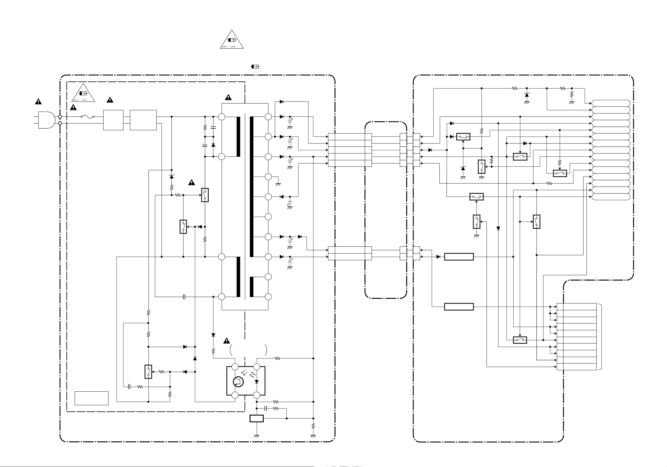
Power Supply Block Diagram
NOTE :
The voltage for parts in hot circuit is measured using
hot GND as a common terminal.
HOT CIRCUIT. BE CAREFUL.
F
F
A V
CAUTION
FOR CONTINUED PROTECTION AGAINST FIRE HAZARD,
REPLACE ONLY WITH THE SAME TYPE FUSE.
ATTENTION : POUR UNE PROTECTION CONTINUE LES RISQES
D'INCELE N'UTILISER QUE DES FUSIBLE DE MEMO TYPE.
RISK OF FIRE
"This symbol means fast operating fuse."
"Ce symbole reprèsente un fusible à fusion rapide."
-REPLACE FUSE AS MARKED.
CAUTION !
Fixed voltage ( or Auto voltage selectable ) power supply circuit is used in this unit.
If Main Fuse (F001) is blown, check to see that all components in the power supply
circuit are not defective before you connect the AC plug to the AC power supply.
Otherwise it may cause some components in the power supply circuit to fail.
AC1001
A V
F1001
1A 250V
L1001
LINE
FILTER
D1001 - D1004
BRIDGE
RECTIFIER
Q1003
Q1001
T001
2
4
8
20
19
18
17
16
15
14
13
CL1002
1 1AL+44V
2 2P-DOWN-L
3 3AL+12V
5 5AL+5V
7 7AL-24V
CL1006 CL1007
1 1AL+2.35V
3 3AL+4V
CL1004 CN1005
CN1003
1
1
2
2
3
3
5
5
7
7
CN1005 CN1003
9
9
11
11
Q055
Q1005
IC1004
+3.3V REG.
Q057
Q052
Q056
Q1006
Q1011
AL+15V
AL+33V
P-DOWN-L
AL+12V
P-ON+9V
AL+5V
TIMER+5V
AL-24V
P-ON-L
P-ON+5V
-FL
DVD-P-ON+3.3V
DVD-P-ON+5V
EV+3.3V
DVD-P-ON+12V
HOT
POWER SUPPLY CBA
Q1008
7
IC1001
ERROR
VOLTAGE DET
4
IC1006
(SHUNT REGULATOR)
1
23
REG
12
11
JUNCTION
CBA
IC1002
+1.5V REG.
MAIN CBA
Q1004
CN1001
1 EV+1.5V
2 EV+1.5V
3 EV+1.5V
4 EV+3.3V
5 EV+3.3V
13 DVD-P-ON+5V
14 EV+9V
15 EV+9V
17 DVD-P-ON+3.3V
19 PWRCON
TO DVD MAIN
CBA UNIT
CN401
H9411BLP1-10-7 1-10-8
Page 28
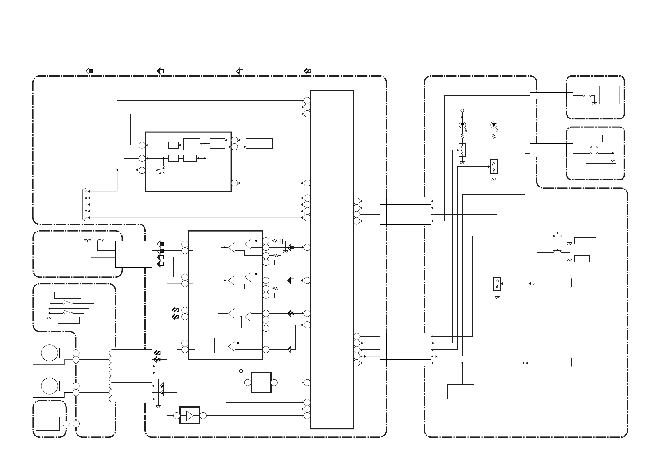
DVD System Control/Servo Block Diagram
BLOCK DIAGRAMS <DVD SECTION>
TO
DVD VIDEO/ AUDIO
BLOCK DIAGRAM
PICK-UP
UNIT
FOCUS SERVO SIGNAL TRACKING SERVO SIGNAL
IC451
(CLOCK GENERATOR)
1/4
1/4
MULTI
PLL
PLL2
IC301
(SERVO DRIVE)
FOCUS
15
ACTUATOR
DRIVE
16
PCM-SCLK
DVD-A-MUTE
ADAC-MD
ADAC-MC
ADAC-ML
FSTS
3
15
10
CN201
FS(+) 18
FS(-) 19
TS(+) 20
TS(-) 17
X'TAL
OSC
SLED SERVO SIGNAL SPINDLE SERVO SIGNAL
IC101
(MICRO CONTROLLER)
EXT CLOCK
172
CLK33M
BE CLOCK
170
X451
7
36.864MHz
OSC
8
14
27
+
-+
-
26
25
24
1792FSEL
95
DVD-A-MUTE
ADAC-MD
51
50 ADAC-MC
96 ADAC-ML
152
FOCUS DRIVE
POWER
/CLOSE
PLAY
STOP
OPEN
48
47
62
94
CN302
SW2001
DVD
OPEN
/CLOSE
OPEN/CLOSE
CL2002CL2003
22
DVD
AL+5V
D2001
DISC IN
Q2002
D2002
PLAY
CL2007 CL2006
STOP 11
SKIP-DOWN 22
Q2003
OPEN/CLOSE CBA
SW2005
STOP
SW2006
SKIP DOWN
DVD SW CBA
CN2001
PLAY 11
STOP 22
POWER 33
OPEN/CLOSE 44
SW2003
SKIP-UP
SW2002
PLAY
SPINDLE
MOTOR
M
SLED
MOTOR
M
FG CBA
FG
SENSOR
TRAY-OUT
TRAY-IN
CN3002 CN301
DRIVE CBA
TRACKING
14
ACTUATOR
DRIVE
13
SPINDLE
12
MOTOR
DRIVE
11
SLED
17
MOTOR
DRIVE
3SP(+)
4SP(-)
5TRAY-OUT
6TRAY-IN
7GND
8SL(-)
9SL(+)
1FG-IN
18
IC202
(OP AMP)
12 14
DVD MAIN CBA UNIT
+
-
+
-
+
-
+3.3V
+
-
1
2
3
4
+
-
5
6
23
IC461
RESET
5 4
TRACKING
150
DRIVE
SPDL71
SLD70
RESET68
TRAY-OUT
97
TRAY-IN
60
FG-IN
66
SKIP-UP
FP-STB
FP-DIN 54
FP-CLK
REMOTE-DVD
55
59
53
61
CN401
SKIP-UP
FP-STB
FP-DIN 1818
FP-CLK
REMOTE-DVD 2222
Q2001
DVD-POWER
CN1001
2020
1616
2121
REMOTE-VIDEO
RM2001
REMOTE
SENSOR
MAIN CBA
FROM SERVO
/SYSTEM CONTROL
BLOCK DIAGRAM
<VCR SECTION>
FROM/TO SERVO
/SYSTEM CONTROL
BLOCK DIAGRAM
<VCR SECTION>
1-10-9
1-10-10
H9411BLSD
Page 29
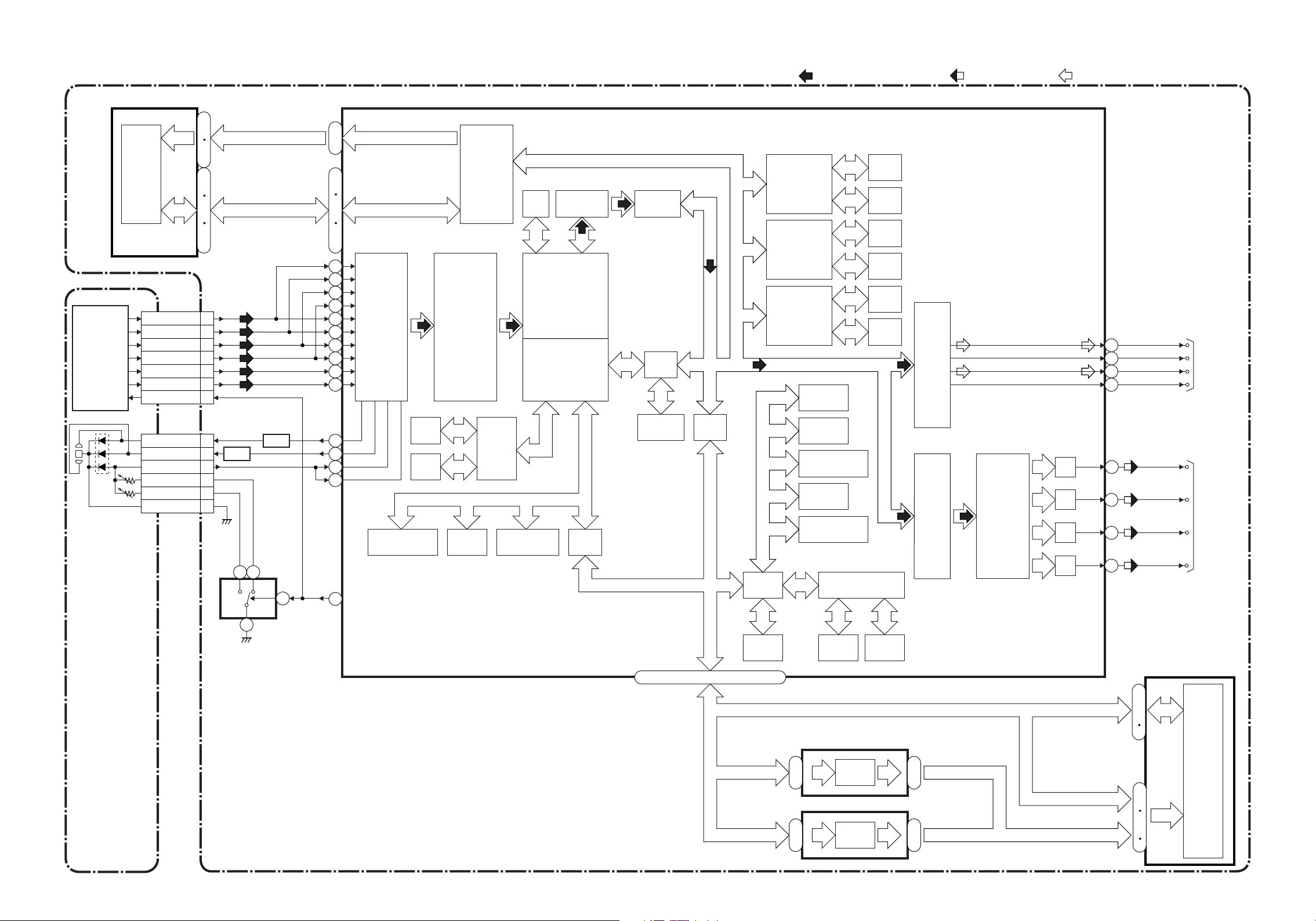
Digital Signal Process Block Diagram
IC102 (SDRAM) IC101 (MICRO CONTROLLER)
24
DETECTOR
SDRAM
27
60
66
13
31
56
74
85
C 6
D 7
A 8
B 5
F 10
E 2
CD/DVD 9
~~
2
~~~
CN201
210
235
2
13
184
205
247
256
124
125
122
123
128
129
126
127
131
130
~
~~~
SDRAM ADDRESS(0-10)SDRAM ADDRESS(0-10)
SDRAM DATA(0-31)SDRAM DATA(0-31)
RF
SIGNAL
PROCESS
CIRCUIT
EXTERNAL
MEMORY
I/F
DVD/CD
FORMATTER
ECC
DECODER
I/F
DMA
BCU
STREAM
I/F
UMAC
DATA(VIDEO/AUDIO) SIGNAL DVD VIDEO SIGNAL
DSP
DECODER
PIXEL
OPERATION
I/O
PROCESSOR
SERIAL
DATA
ROM
INST.
ROM
DATA
ROM
INST.
ROM
DATA
ROM
INST.
ROM
AUDIO
I/F
DATA(AUDIO) SIGNAL
181
175
176
174
SPDIF
PCM-BCK
PCM-DATA0
PCM-LRCLK
TO DVD
VIDEO
/AUDIO
BLOCK
DIAGRAM
PICK UP
UNIT
CD-LD 12
DVD-LD 14
PD-MONI 13
GND(DVD-PD)
GND(CD-PD)
GND(LD)
CN201
15
16
11
Q253,Q254
AMP
AMP
Q251,Q252
1 3
CD DVD
4
6
IC201
(SW)
DVD MAIN CBA UNIT
135
133
132
134
78
INTERRUPT
CONTROLLER
CD/DVD
INST.
ROM
DATA
ROM
TIMER
32BIT
CPU
WATCH DOG
TIMER
CPU
I/F
READ
MEMORY
EXT ADT (0-15), EXT ADR (16-19)
CPU
I/F
BCU
DEBUG
EXT ADT (0-15), EXT ADR (16-19)
EXT ADT (0-7)
EXT ADT (8-15)
GENERAL
I/O
INTERRUPT
CONTROLLER
TIMER
WATCH DOG
TIMER
INST
CACHE
IC105 (LATCH)
2
~
9
IC104 (LATCH)
2
~
9
32BIT CPU
DATA
CACHE
D TYPE
LATCH
D TYPE
LATCH
VIDEO
I/F
12
~
EXT ADR (0-7)
19
12
~
EXT ADR (8-15)
19
NTSC/PAL
ENCODER
D/A
D/A
D/A
D/A
EXT ADT (0-15)
EXT ADR (16-19)
EXT ADR (0-15)
Y
C
Cr
Cb
158
164
161
160
VIDEO-Y
VIDEO-C
VIDEO-Cr
VIDEO-Cb
IC103 (FLASH ROM)
29
~~
36
38
45
FLASH
ROM
1
~
9
16
~
25
48
TO DVD
VIDEO
/AUDIO
BLOCK
DIAGRAM
1-10-11
1-10-12
H9411BLD
Page 30
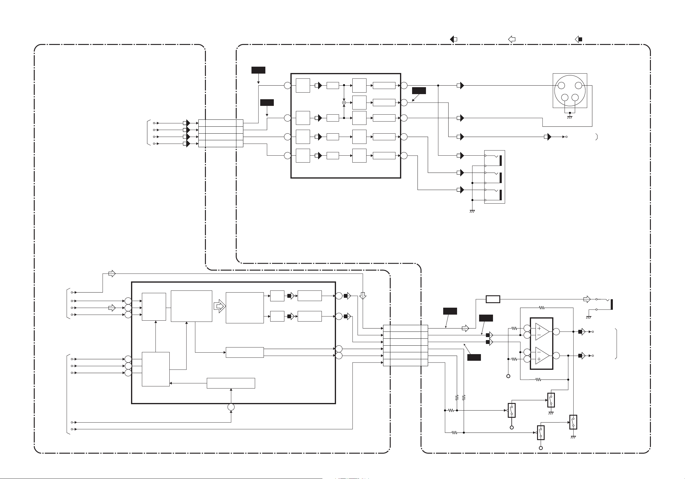
DVD Video / Audio Block Diagram
DVD VIDEO SIGNAL
DVD AUDIO SIGNALDATA(AUDIO) SIGNAL
FROM DIGITAL
SIGNAL PROCESS
BLOCK DIAGRAM
VIDEO-Y
VIDEO-C
VIDEO-Cb
VIDEO-Cr
CN601
5 5VIDEO-Y
7 7VIDEO-C
3 3VIDEO-Cb
1 1VIDEO-Cr
CN1601
WF4
WF5
IC1402 (VIDEO DRIVER)
11
4dB
6
AMP
4dB
2
AMP
4dB
9
AMP
4dB
AMP
LPF DRIVER
LPF DRIVER
LPF DRIVER
LPF DRIVER
2dB
AMP
2dB
AMP
2dB
AMP
2dB
AMP
2dB
AMP
DRIVER
18
21
23
15
13
WF6
JK1403
VIDEO-Y
OUT
VIDEO-Cb
OUT
VIDEO-Cr
OUT
Y
C
3 4
1
2
DVD-VIDEO TO VIDEO
JK1401
S-VIDEO OUT
BLOCK DIAGRAM
<VCR SECTION>
FROM
DIGITAL
SIGNAL
PROCESS
BLOCK
DIAGRAM
FROM
DVD
SYSTEM
CONTROL
/SERVO
BLOCK
DIAGRAM
SPDIF
PCM-BCK
PCM-DATA0
PCM-LRCLK
ADAC-MD
ADAC-MC
ADAC-ML
PCM-SCLK
A-MUTE
IC601 (AUDIO DAC)
1
2
3
13
14
15
SERIAL
PORT
SERIAL
CONTROL
4X/8X
OVERSAMPLING
DIGITAL FILTER
/FUNCTION
CONTROLLER
ENPHANCED
MULTI-LEVEL
DELTA-SIGMA
MODULATOR
ZERO DETECT
SYSTEM CLOCK
16
DAC
DAC
LPF+AMP
LPF+AMP
L-CH
R-CH
12
11
WF8
Q1351
WF7
AMP
VREF
Q1204
+3.3V
IC1201
3
2
6
5
(AMP)
1
7
Q1202
Q1203
7
8
CN601 CN1601
1616SPDIF
11 11DVD-A(L)
1313DVD-A(R)
12 12
DVD-A(L)-MUTE
14 14
DVD-A(R)-MUTE
10 10
DVD-A-MUTE
WF9
Q1201
JK1202
DVD-A(L)
DVD-A(R)
DIGITAL
AUDIO OUT
TO
Hi-Fi AUDIO
BLOCK
DIAGRAM
<VCR
SECTION>
MAIN CBADVD MAIN CBA UNIT
+3.3V
1-10-13 1-10-14
H9411BLVD
Page 31

SCHEMATIC DIAGRAMS / CBA’S AND TEST POINTS
Standard Notes
WARNING
Many electrical and m echanical parts in this chassis
have special characteristics. These characteristics
often pass unnoticed and the protection afforded by
them cannot necessarily be obtained by using replacement components rated for higher voltage, wattage,
etc. Replacement par ts that have these specia l safety
characteristics are identified in this manual and its
supplements; electr ical components having such features are identified by the mark " # " in the schematic
diagram and the parts list. Before replacing any of
these components, read the par ts list in this manual
carefully. The use of substitut e replacem ent par t s that
do not have the same safety characteristics as specified in the parts list may create shock, fire, or other
hazards.
Notes:
1. Do not use the part number shown on these drawings for ordering. The correct part number is shown
in the parts list, and may be slightly different or
amended since these drawings were prepared.
2. All resistance values are indicated in ohms
3
(K=10
3. Re sistor wattages are 1/4W or 1/6W unless otherwise specified.
4. All capacitance values are indicated in µF
(P=10
5. All voltages are DC voltages unless otherwise
specified.
, M=106).
-6
µF).
1-11-1 H9400SC
Page 32

LIST OF CAUTION, NOTES, AND SYMBOLS U SED IN THE SCHEMATIC DIAGRAMS ON THE FOLLOWING
PAGES:
1. CAUTION:
FOR CONTINUED PROTECTION AGAINST FIRE HAZARD, REPLACE ONLY WITH THE SAME
F
A V
TYPE FUSE.
ATTENTION: POUR UNE PROTECTION CONTINUE LES RISQES D'INCELE N'UTILISER QUE
DES FUSIBLE DE MEMO TYPE.
RISK OF FIRE-REPLACE FUSE AS MARKED.
This symbol means fast operating fuse.
Ce symbole represente un fusible a fusion rapide.
2. CAUTION:
Fixed Voltage (or Auto voltage selectable) power supply circuit is used in this unit.
If Main Fuse (F001) is blown, first check to see that all components in the power supply circuit are not defective
before you connect the AC plug to the AC power supply. Other wise it may cause some components in the
power supply circuit to fail.
3. Note:
(1) Do not use the part number shown on the drawings for ordering. The correct part number is shown in the parts
list, and may be slightly different or amended since the drawings were prepared.
(2) To maintain original function and reliability of repaired units, use only original replacement parts which are listed
with their part numbers in the parts list section of the service manual.
4. Wire Connectors
(1) Prefix symbol "CN" means "connector" (can disconnect and reconnect).
(2) Prefix symbol "CL" means "wire-solder holes of the PCB" (wire is soldered directly).
5. Mode: SP/REC
6. Voltage indications for PLAY and REC modes on the schematics are as shown below:
< DVD Section >
5.0
The same voltage for
both PLAY & STOP modes
5.0
(2.5)
PLAY mode
STOP mode
231
Indicates that the voltage
is not consistent here.
The same voltage for
both PLAY, REC & DVD
modes
< VCR Section >
231
5.0
5.0
(2.5)
< >
Indicates that the voltage
is not consistent here.
PLAY mode
REC mode
DVD mode
7. How to read converged lines
1-D3
Distinction Area
3
AREA D3
Line Number
(1 to 3 digits)
2
AREA B1
Examples:
1. "1-D3" means that line number "1" goes to area "D3".
1
1-D3
2. "1-B1" means that line number "1" goes to area "B1".
ABCD
8. Test Point Information
: Indicates a test point with a jumper wire across a hole in the PCB.
Unit: Volts
1-B1
: Used to indicate a test point with a component lead on foil side.
: Used to indicate a test point with no test pin.
: Used to indicate a test point with a test pin.
1-11-2 SC_09
Page 33

Main 1/7 Schematic Diagram < VCR Section >
MAI N 1/7 Schematic Diagram
Part s Loc ation Guide
Ref No. Position
IC501 C-3
Q501 D-1
Q506 A-3
CL501 A-4
CL502 F-4
CL504 A-4
VR501 B-4
TP505 B-3
TP513 B-4
TEST POINTS
TRANSISTORS
VARI A B LE RE S I S T ORS
CONNECTORS
ICS
REC VIDEO SIGNAL
REC AUDIO SIGNAL
PB VIDEO SIGNAL
PB AUDIO SIGNAL
A4
A3
B4
B3
C4
C3
D4
D3
E4
E3
F4
F3
A2
A1
B2
B1
1-11-3
C2
C1
D2
D1
E2
E1
1-11-4
F2
F1
H9411SCM1
Page 34

Main 2/7 Schematic Diagram < VCR Section >
MAI N 2/7 Schematic Diagram
Parts Location Guide
Ref No. Position
L701 H-1
Q503 L-1
Q504 L-1
Q563 H-3
Q565 H-3
Q566 I-3
Q567 I-3
TP502 I-4
TP506 K-1
TP507 K-1
TEST POINTS
TRANSISTORS
COILS
1
Note:
*
When it is necessary to replace one or more of the following Diodes,
all four should be replaced: D564, D565, D566, D567.
REC VIDEO SIGNAL
REC AUDIO SIGNAL
DVD VIDEO + PB VIDEO SIGANL
PB AUDIO SIGNAL
DVD AUDIO SIGNAL
G4
G3
H4
H3
I4
I3
J4
J3
K4
K3
L4
L3
G2
G1
1-11-5
H2
H1
I2
I1
J2
J1
K2
K1
1-11-6
L2
L1
H9411SCM2
Page 35

Main 3/7 Schematic Diagram < VCR Section >
MAI N 3/7 Schematic Diagram
Part s Loc ation Guide
Ref No. Position
IC301 N-2
Q301 Q-3
Q302 Q-4
Q303 Q-4
Q391 P-1
Q421 N-1
Q422 N-1
Q423 N-1
Q424 N-1
Q425 N-1
CL253 M-4
TP301 O-4
TP302 P-1
TRANSISTORS
TEST POINTS
CONNECTORS
ICS
REC VIDEO SIGNAL
REC AUDIO SIGNAL
PB VIDEO SIGNAL
DVD VIDEO + PB VIDEO SIGNAL
PB AUDIO SIGNAL
M4
M3
N4
N3
O4 P4 Q4 R4
O3
P3
Q3
R3
M2
M1
N2
N1
1-11-7
O2
O1
P2
P1
Q2
Q1
1-11-8
R2
R1
H9411SCM3
Page 36

Main 4/7 Schematic Diagram < VCR Section >
MAI N 4/7 Schematic Diagram
Part s Loc ation Guide
Ref No. Position
IC1201 Y-1
IC1402 Z-3
L1350 Z-2
L1351 BB-1
L1401 AA-1
L1441 AA-1
L1442 AA-1
L1461 AA-1
L1481 AA-1
L1521 Y-2
Q1201 Z-1
Q1202 Z-1
Q1203 Z-1
Q1204 Z-1
Q1351 AA-1
Q1385 Y-2
CN1601 X-3
TRANSISTORS
COILS
CONNECTORS
ICS
X3
Y3
Z3
DVD VIDEO SIGNAL
DVD AUDIO SIGNAL
AA3
DATA (AUDIO) SIGNAL
BB3
X2
X1
1-11-9
Y2
Y1
Z2
Z1
AA2
AA1
BB2
BB1
1-11-10
H9411SCM4
Page 37

Main 5/7 Schematic Diagram < VCR Section >
MAIN 5/7 Schemat i c D i agram
Part s Loc ation Guide
Ref No. Posit io n
IC751 DD-3
Q760 CC-3
Q762 DD-2
Q763 DD-2
TP751 EE-2
TP753 EE-2
TP754 EE-2
TEST POINTS
ICS
TRANSISTORS
CC4
CC3
DD4
DD3
EE4
EE3
REC VIDEO SIGNAL
REC AUDIO SIGNAL
FF4
FF3
DVD VIDEO SIGNAL
PB VIDEO SIGNAL
PB AUDIO SIGNAL
DVD AUDIO SIGNAL
CC2
CC1
DD2
DD1
1-11-11
EE2
EE1
FF2
FF1
1-11-12
H9411SCM5
Page 38

Main 6/7 Schematic Diagram < VCR Section >
MAIN 6/7 Schemat i c D i agram
Part s Loc ation Guide
Ref No. Posit io n
L2001 KK-1
Q2001 II-2
Q2002 HH-2
Q2003 HH-1
CN2001 GG-3
CONNECTORS
COILS
TRANSISTORS
2
Note:
*
When it is necessary to replace one or more of the following Diodes,
all two should be replaced: D2001, D2002.
GG4
GG3
HH4
HH3
II4 JJ4 KK4
II3
JJ3
KK3
LL4
LL3
GG2
GG1
1-11-13
HH2
HH1
II2
II1
JJ2
JJ1
KK2
KK1
1-11-14
LL2
LL1
H9411SCM6
Page 39

Main 7/7 Schematic Diagram < VCR Section >
MAI N 7/7 Schematic Diagram
Part s Loc ation Guide
Ref No. Position
IC1002 NN-3
IC1004 OO-1
L1009 OO-1
L1010 OO-2
Q052 QQ-4
Q055 PP-3
Q056 QQ-3
Q057 PP-3
Q1004 PP-1
Q1005 NN-2
Q1006 OO-2
Q1011 NN-1
CN1001 MM-3
CN1003 MM-4
COILS
CONNECTORS
TRANSISTORS
ICS
MM4
MM3
NN4
NN3
OO4 PP4 QQ4
OO3
PP3
QQ3
RR4
RR3
MM2
MM1
NN2
NN1
1-11-15
OO2
OO1
PP2
PP1
QQ2
QQ1
1-11-16
RR2
RR1
H9411SCM7
Page 40

Power Supply Schematic Diagram < VCR Section >
Power Supply Schematic Diagram
Part s Loc ation Guide
Ref No. Posit io n
IC1001 C-1
IC1006 D-1
L003 B-4
L009 D-3
L1001 A-4
L1007 D -2
L1020 D -2
Q1001 C-3
Q1003 B-3
Q1008 B-2
COILS
TRANSISTORS
ICS
F
A V
CAUTION
FOR CONTINUED PROTECTION AGAINST FIRE HAZARD,
REPLACE ONL Y WITH THE SAME TYPE FUSE.
ATTENTION : POUR UNE PROTECTION CONTINUE LES RISQES
D'INCELE N'UTILISER QUE DES FUSIBLE DE MÊME TYPE.
RISK OF FIRE-REPLACE FUSE AS MARKED.
"This symbol means fast operating fuse."
"Ce symbole reprèsente un fusible à fusion rapide."
CAUTION !
Fixed voltage ( or Auto voltage selectable ) power supply circuit is used in this unit.
If Main Fuse (F1001) is blown, check to see that all components in the power supply
circuit are not defective before you connect the AC plug to the AC power supply.
Otherwise it may cause some components in the power supply circuit to fail.
NOTE :
The voltage for parts in hot circuit is measured using
hot GND as a common terminal.
A4
A3
B4
B3
C4 D4
C3
D3
E4 F4
E3
F3
A2
A1
1-11-17
B2
B1
C2
C1
D2
D1
E2
E1
1-11-18
F2
F1
H9411SCP
Page 41

Function Schematic Diagram < VCR Section >
3
Note:
*
When it is necessary to replace one or more of the following Diodes,
all one should be replaced: D561.
A2
A1
B2
B1
C2
C1
1-11-19 1-11-20 H9411SCF
Page 42

Main CBA Top View
Sensor CBA Top View
BHB300F01014-A
BHB300F01014-B
WF1
TP751
V-OUT
TP513
CTL
WF2
TP302
RF-SW
WF3
TP301
C-PB
1-11-21
1-11-22
VR501
SW-P
TP502
S-INH
BH9400F01014A
Page 43

Main CBA Bottom View
MAIN CBA Parts Location Guide
Ref No. Position Ref No. Position Ref No. Position Ref No. Position Ref No. Position Ref No. Position
TRANSISTORSICS TRANSISTORS
IC301 C-3 Q057 C-4 Q506 C-2 Q1202 B-4 CL509 E-3 TP502 D-1
IC451 C-3 Q301 C-2 Q563 C-1 Q1203 A-3 CL2003 B-1 TP505 B-2
IC501 C-2 Q302 C-2 Q565 C-1 Q1204 A-2 CL2007 A-1 TP506 E-3
IC571 A-1 Q303 C-2 Q566 C-1 Q1351 A-4 CN1001 A-2 TP507 B-3
IC751 B-2 Q391 E-4 Q567 C-1 Q1385 A-2 CN1003 A-4 TP513 E-3
IC1002 A-4 Q421 C-3 Q760 B-2 Q2001 A-1 CN1601 A-3 TP751 E-4
IC1004 A-3 Q422 B-3 Q762 D-4 Q2002 A-1 CN2001 A-1 TP753 E-4
IC1201 A-3 Q423 C-4 Q763 D-4 Q2003 A-1 TP754 E-4
IC1402 A-4 Q424 C-4 Q1004 B-3 VR501 E-2
TRANSISTORS
Q052 C-4 Q501 C-1 Q1006 A-3 CL501 B-3 TP301 B-2
Q055 C-4 Q503 B-3 Q1011 A-3 CL502 E-3 TP302 E-3
Q056 C-4 Q504 E-3 Q1201 A-4 CL504 D-3 TP452 B-3
Q425 C-4 Q1005 A-3 CL253 C-3
TRANSISTORS
CONNECTORS
CONNECTORS
VARIABLE RESISTORS
TEST POINTS
TEST POINTS
1-11-23
1-11-24
BH9400F01014A
Page 44

Function CBA Top View
Function CBA Bottom View
BH9400F01014B
DVD OPEN/CLOSE CBA
Top View
DVD OPEN/CLOSE CBA
Bottom View
BH9400F01014C
DVD SW CBA Top View DVD SW CBA Bottom View
BH9400F01014D
1-11-25
1-11-26
Page 45

Power Supply CBA Top View
Power Supply CBA
Parts Location Guide
Ref No. Position
IC1001 B-1
IC1006 B-1
Q1001 B-1
Q1003 A-2
Q1008 A-2
CL1002 C-2
CL1006 C-1
TRANSISTORS
ICS
CONNECTORS
Power Supply CBA Bottom View
F
A V
CAUTION
FOR CONTINUED PROTECTION AGAINST FIRE HAZARD,
REPLACE ONLY WITH THE SAME TYPE FUSE.
ATTENTION : POUR UNE PROTECTION CONTINUE LES RISQES
D'INCELE N'UTILISER QUE DES FUSIBLE DE MÊME TYPE.
RISK OF FIRE-REPLACE FUSE AS MARKED.
"This symbol means fast operating fuse."
"Ce symbole reprèsente un fusible à fusion rapide."
L003
CAUTION !
Fixed voltage ( or Auto voltage selectable ) power supply circuit is used in this unit.
If Main Fuse (F1001) is blown, check to see that all components in the power supply
circuit are not defective before you connect the AC plug to the AC power supply.
Otherwise it may cause some components in the power supply circuit to fail.
NOTE :
The voltage for parts in hot circuit is measured
using hot GND as a common terminal.
BECAUSE A HOT CHASSIS GROUND IS PRESENT IN THE POWER
SUPPLY CIRCUIT , AN ISOLATION TRANSFORMER MUST BE USED.
ALSO , IN ORDER TO HAVE THE ABILITY TO INCREASE THE INPUT
SLOWLY , WHEN TROUBLESHOOTING THIS TYPE POWER SUPPLY
CIRCUIT , A VARIABLE ISOLATION TRANSFORMER IS REQUIRED.
NOTE :
Either BH9400F01021, BH9400F01022
is used for the Power Supply CBA in this S/M.
Junction CBA Top View Junction CBA Bottom View
1-11-27
BH9400F01021A
NOTE :
Either BH9400F01021, BH9400F01022
is used for the Junction CBA in this S/M.
BH9400F01021B
1-11-28
Page 46

Power Supply CBA Top View
Power Supply CBA
Parts Location Guide
Ref No. Position
IC1001 B-1
IC1006 B-1
Q1001 B-1
Q1003 A-2
Q1008 A-2
CL1002 C-2
CL1006 C-1
TRANSISTORS
ICS
CONNECTORS
Power Supply CBA Bottom View
F
A V
CAUTION
FOR CONTINUED PROTECTION AGAINST FIRE HAZARD,
REPLACE ONLY WITH THE SAME TYPE FUSE.
ATTENTION : POUR UNE PROTECTION CONTINUE LES RISQES
D'INCELE N'UTILISER QUE DES FUSIBLE DE MÊME TYPE.
RISK OF FIRE-REPLACE FUSE AS MARKED.
"This symbol means fast operating fuse."
"Ce symbole reprèsente un fusible à fusion rapide."
L003
CAUTION !
Fixed voltage ( or Auto voltage selectable ) power supply circuit is used in this unit.
If Main Fuse (F1001) is blown, check to see that all components in the power supply
circuit are not defective before you connect the AC plug to the AC power supply.
Otherwise it may cause some components in the power supply circuit to fail.
NOTE :
The voltage for parts in hot circuit is measured
using hot GND as a common terminal.
BECAUSE A HOT CHASSIS GROUND IS PRESENT IN THE POWER
SUPPLY CIRCUIT , AN ISOLATION TRANSFORMER MUST BE USED.
ALSO , IN ORDER TO HAVE THE ABILITY TO INCREASE THE INPUT
SLOWLY , WHEN TROUBLESHOOTING THIS TYPE POWER SUPPLY
CIRCUIT , A VARIABLE ISOLATION TRANSFORMER IS REQUIRED.
NOTE :
Either BH9400F01021, BH9400F01022
is used for the Power Supply CBA in this S/M.
Junction CBA Top View Junction CBA Bottom View
1-11-29
BH9400F01022A
NOTE :
Either BH9400F01021, BH9400F01022
is used for the Junction CBA in this S/M.
BH9400F01022B
1-11-30
Page 47

DVD Main 1/3 Schematic Diagram < DVD Section >
DVD MAIN 1/3 Sc hematic Diagram
Part s Loc ation Guide
Ref No. Position
IC201 B-1
IC202 E-4
IC301 D-3
IC461 E-1
Q251 C-2
Q252 B-2
Q253 C-2
Q254 B-2
ICS
TRANSISTORS
DATA(VIDEO+AUDIO)
TRACKING SERVO SIGNAL
SLIDE SERVO SIGNAL
A4
A3
B4
B3
C4
C3
FOCUS SERVO SIGNAL
D4
D3
SPINDLE SERVO SIGNAL
E4
E3
F4
F3
A2
A1
B2
B1
1-11-31 1-11-32
C2
C1
D2
D1
E2
E1
F2
F1
H9411SCD1
Page 48

DVD Main 2/3 Schematic Diagram < DVD Section >
DVD MAIN 2/3 Schematic Diagram
Part s Loc ation Guide
Ref No. Position
IC101 H-4
ICS
DATA(VIDEO+AUDIO)
TRACKING SERVO SIGNAL
SLIDE SERVO SIGNAL
G4
G3
H4
H3
I4
I3
FOCUS SERVO SIGNAL
SPINDLE SERVO SIGNAL
J4
J3
K4
K3
L4
L3
G2
G1
H2
H1
1-11-33 1-11-34
I2
I1
J2
J1
K2
K1
L2
L1
H9411SCD2
Page 49

IC101 V OLTA GE CHA RT
PIN.NO PLAY STOP PIN.NO PLAY STOP PIN.NO PLAY STOP PI N.NO PLAY STOP
129 2.0 2.0 161 0.5 0.5 193 ~ ~ 225 1.9 1.9
130 2.2 2.2 162 1.4 1.4 194 0 0 226 3.3 3.3
131 2.3 2.3 163 ----- ----- 195 3.3 3.3 227 ~ ~
132 0.4 0.1 164 0.9 0.9 196 ~ ~ 228 ~ ~
133 1.2 0.4 165 3.3 3.3 197 ~ ~ 229 ~ ~
134 0.4 0.1 166 1.5 1.5 198 0 0 230 0 0
135 0.2 0.2 167 0 0 199 ~ ~ 231 ----- ----136 2.3 2.3 168 2.1 2.1 200 ~ ~ 232 3.3 3.3
137 1.7 1.7 169 0 0 201 ~ ~ 233 3.3 3.3
138 0 0 170 0.8 0.8 202 3.3 3.3 234 1.6 1.6
139 1.7 1.7 171 3.3 3.3 203 ~ ~ 235 ~ ~
140 1.7 1.7 172 1.6 1.6 204 ~ ~ 236 0 0
141 1.7 1.7 173 ----- ----- 205 ~ ~ 237 1.7 1.7
142 1.7 1.7 174 1.8 1.8 206 0 0 238 3.0 3.0
143 0.5 0.5 175 1.7 1.7 207 2.4 3.5 239 3.3 3.3
144 1.6 1.6 176 1.4 0.1 208 2.4 2.1 240 3.3 3.3
145 3.3 3.3 177 0 0 209 3.3 3.3 241 0 0
146 0 0 178 ----- ----- 210 ~ ~ 242 3.2 3.2
147 ----- ----- 179 ----- ----- 211 0 0 243 2.4 2.1
148 ----- ----- 180 ----- ----- 212 ~ ~ 244 1.5 1.5
149 3.3 3.3 181 1.7 1.7 213 1.5 1.5 245 0 0
150 1.7 1.7 182 3.3 3.3 214 ~ ~ 246 2.4 2.1
151 0 0 183 0 0 215 0 0 247 ~ ~
152 1.7 1.7 184 ~ ~ 216 ~ ~ 248 0 0
153 3.3 3.3 185 ~ ~ 217 ~ ~ 249 ~ ~
154 1.4 1.4 186 1.5 1.5 218 3.3 3.3 250 3.3 3.3
155 0 0 187 ~ ~ 219 ~ ~ 251 ~ ~
156 2.2 2.2 188 ~ ~ 220 ~ ~ 252 ~ ~
157 3.3 3.3 189 3.3 3.3 221 0 0 253 ~ ~
158 0.7 0.7 190 ~ ~ 222 1.5 1.5 254 0 0
159 0 0 191 ~ ~ 223 1.9 1.9 255 ~ ~
160 0.5 0.5 192 ~ ~ 224 0 0 256 ~ ~
PIN.NO PLAY STOP PIN.NO PLAY STOP PIN.NO PLAY STOP PI N.NO PLAY STOP
1 3.33.3332.22.9650.10.1973.43.4
2~~34~~661.22.5981.61.6
3~~35~~671.61.6990 0
4 0 0 36 ~ ~ 68 3.4 3.4 100 ----- ----5 ~ ~ 37 ~ ~ 69 0 0 101 ----- ----6 ~ ~ 38 0.3 0.5 70 1.7 1.7 102 ----- ----7 3.3 3.3 39 0.1 0.1 71 2.4 1.7 103 ----- ----8 ~ ~ 40 ~ ~ 72 ----- ----- 104 3.3 3.3
9 ~ ~ 41 ~ ~ 73 ----- ----- 105 0.9 0.9
10 ~ ~ 42 3.3 3.3 74 ----- ----- 106 0 0
11 0 0 43 0 0 75 3.4 3.4 107 0.8 0.8
12 ~ ~ 44 ~ ~ 76 ----- ----- 108 1.6 1.6
13 ~ ~ 45 ~ ~ 77 ----- ----- 109 2.1 2.1
14 3.3 3.3 46 2.0 2.6 78 0.1 0.1 110 2.6 2.6
15 1.5 1.5 47 3.3 3.4 79 3.3 3.3 111 2.0 2.0
16 0 0 48 3.2 3.4 80 0 0 112 0.7 0.9
17 3.4 3.4 49 ----- ----- 81 ----- ----- 113 0 0
18 3.4 3.4 50 3.4 3.4 82 ----- ----- 114 1.8 1.8
19 ~ ~ 51 3.4 3.4 83 ----- ----- 115 1.4 1.4
20 ~ ~ 52 ----- ----- 84 ----- ----- 116 0.3 0.3
21 ~ ~ 53 3.4 3.4 85 ----- ----- 117 1.6 1.6
22 ~ ~ 54 3.4 3.4 86 ----- ----- 118 3.3 3.3
23 3.3 3.3 55 3.3 3.3 87 ----- ----- 119 0 0
24 0 0 56 3.3 3.3 88 ----- ----- 120 1.9 1.9
25 0.4 0.4 57 0 0 89 ----- ----- 121 1.9 1.9
26 0.9 0.6 58 0 0 90 ----- ----- 122 2.4 2.4
27 ~ ~ 59 3.3 3.3 91 3.3 3.3 123 2.4 2.4
28 ~ ~ 60 3.4 3.4 92 1.7 1.5 124 2.4 2.4
29 3.3 3.3 61 3.1 3.1 93 0 0 125 2.4 2.4
30 0 0 62 3.2 3.4 94 ----- ----- 126 2.0 2.0
31 ~ ~ 63 3.4 3.4 95 3.4 0.1 127 2.0 2.0
32 ~ ~ 64 ----- ----- 96 3.4 3.4 128 2.0 2.0
1-11-35
1-11-36
Page 50

DVD Main 3/3 Schematic Diagram < DVD Section >
DVD MAIN 3/3 Schematic Diagram
Part s Loc ation Guide
Ref No. Position
IC102 O-4
IC103 O-3
IC104 N-3
IC105 N-1
IC451 P-3
IC601 Q-1
ICS
VIDEO SIGNAL
SPINDLE SERVO SIGNAL
DATA(AUDIO)
M4
M3
N4
N3
O4 P4 Q4 R4
O3
P3
Q3
R3
M2
M1
1-11-37
N2
N1
O2
O1
P2
P1
Q2
Q1
1-11-38
R2
R1
H9411SCD3
Page 51

WAVEFORMS
(TP751 of Main CBA)
WF 1
V-OUT E-E
10usec 50mV x 10
WF1
UPPER
WF2
LOWER
V-OUT 0.1V x 10
RF-SW 0.5V x 10
(TP751 of Main CBA)
(TP302 of Main CBA)
50usec
WF4 Pin 5 of CN1601
VIDEO-Y 0.2V 20µsec
WF5 Pin 7 of CN1601
VIDEO-C 0.2V 20µsec
WF3
UPPER
WF2
LOWER
C-PB 10mV x 10
RF-SW 0.5V x 10
(TP301 of Main CBA)
(TP302 of Main CBA)
5msec
WF6 Pin 21 of IC1402
VIDEO-CVBS 0.5V 20µsec
1-12-1 H9411WF
Page 52

WF7
Pin 11 of CN1601
WAVEFORMS
WF10
(Pin 2 of TU701)
WF13
(Pin 12 of TU701)
AUDIO-L
WF8
Pin 13 of CN1601
AUDIO-R
WF9
Pin 16 of CN1601
1V 0.5msec
1V
MOD-A 20mV x 10 0.2msec
WF11
(Pin 6 of TU701)
MOD-V 20mV x 10 2msec
WF12
(Pin 11 of TU701)
PLL-DATA 0.1V x 10 2msec
WF14
WF15
(Pin 14 of TU701)
TU AUDIO 20mV x 10 0.2msec
(Pin 18 of TU701)
SPDIF
1V 0.1µsec
PLL-CLK 0.1V x 10 2msec
1-12-2 H9411WF
TU VIDEO 20mV x 10 10usec
Page 53

FRONT
WIRING DIAGRAM < VCR SECTION >
REAR
(DECK ASSEMBLY)
AC HEAD ASSEMBLY
AUDIO
ERASE HEAD
AUDIO HEAD
CONTROL HEAD
FE HEAD
FULL
ERASE HEAD
MOTOR
CYLINDER ASSEMBLY
PG
SENSOR
DRUM
MOTOR
Hi-Fi AUDIO
(R) HEAD
Hi-Fi AUDIO
(L) HEAD
M
VIDEO
(R)1
HEAD
VIDEO
(L)1
HEAD
VIDEO
(L)2
HEAD
VIDEO
(R)2
HEAD
VIDEOINAUDIO
IN (R)
AUDIO
IN (L)
S-VIDEO
OUT
AUDIO
OUT (R)
AUDIO
OUT (L)
VIDEO
IN
AUDIO
IN (R)
AUDIO
IN (L)
VIDEO
OUT
AUDIO
OUT (R)
AUDIO
OUT (L)
VIDEO-YVIDEO-Cr VIDEO-Cb
DIGITAL
AUDIO OUT
MAIN CBA
CL504
AE-H
1
AE-H/FE-H2
A-COM3
A-PB/REC4
CTL(+)5
6
CTL(-)
CL501
FE-H1
FE-H GND2
CAPSTAN MOTOR
MLOADING
M
CAPSTAN
MOTOR
CL502
1 AL+12V
P-ON+5V
2
3 C-FG
4
C-F/R
C-CONT5
GND
6
LM-FWD/REV
7
D-CONT8
D-PFG9
GND
10
AL+12V
11
AL+15V12
CL253
V(R)-11
V-COM2
3 V(L)-1
V(L)-2
4
V-COM5
V(R)-26
Hi-Fi-A(R)7
Hi-Fi-COM8
Hi-Fi-A(L)9
CN1003 CN1005 CL1002
1AL+44V
1
2
2P-DOWN-L
3
3AL+12V
4
4GND
5
5AL+5V
6GND 6 GND
6
7
7AL-24V
8NU
8
9AL+2.35V
9
10GND
10
11AL+4V
11
12GND
12
13GND
13
14NU
14
15NU
15
JUNCTION CBA
BH9400F01021B
/BH9400F01022B
CL2003 CL2002
GND
1 1
OPEN/CLOSE
2 2
CL509 CL508
POWER-LED
1 1
KEY-1
2 2
GND
3 3
CL2007 CL2006
STOP
1 1
SKIP-DOWN
2 2
GND
3 3
(BH9400F01014A)
CL1004
1 AL+44V
1
2
2 P-DOWN-L
3
3 AL+12V
4
4 GND
5
5 AL+5V
6
7
7 AL-24V
8 NU
8
CL1007
1
2
3
4
5
6
7
CL1006
1 AL+2.35V
2 GND
3 AL+4V
4 GND
5 GND
6 NU
7 NU
SENSOR CBA
(BHB300F01014)
SENSOR CBA
(BHB300F01014)
DVD OPEN/CLOSE CBA
(BH9400F01014C)
FUNCTION CBA
(BH9400F01014B)
DVD SW CBA
(BH9400F01014D)
POWER SUPPLY CBA
BH9400F01021A
/BH9400F01022A
AC CORD
CN1001
EV+1.5V
EV+1.5V
EV+1.5V
EV+3.3V
EV+3.3V
GND
GND
GND
GND
GND
GND
GND
DVD-P-ON+5V
EV+9V
EV+9V
FP-STB
DVD-P-ON+3.3V
FP-DIN
PWRCON
SKIP-UP
FP-CLK
REMOTE-DVD
CN1601
VODEO-Cr
GND
VIDEO-Cb
GND
VIDEO-Y
GND
VIDEO-C
GND
GND
DVD-A-MUTE
DVD-A(L)
DVD-A(L)-MUTE
DVD-A(R)
DVD-A(R)-MUTE
AUDIO+5V
SPDIF
CN2001
PLAY
STOP
POWER
OPEN/CLOSE
ANT-IN
ANT-OUT
1
2
3
4
5
6
7
8
9
10
11
TO DVD
MAIN CBA
12
UNIT CN401
13
14
15
16
17
18
19
20
21
22
1
2
3
4
5
6
7
8
TO DVD
9
MAIN CBA
10
UNIT CN601
11
12
13
14
15
16
1
TO DVD
2
MAIN CBA
3
UNIT CN302
4
TO WIRING
DIAGRAM
<DVD SECTION>
H9411WI1-13-1 1-13-2
Page 54

DVD MECHA
FG
SENSOR
FG CBA
SPINDLE
MOTOR
SLED
MOTOR
WIRING DIAGRAM < DVD SECTION >
CN401
GND
GND
GND
GND
GND
GND
GND
1
2
3
4
5
6
7
8
9
10
11
TO MAIN CBA
12
CN1001
13
14
15
16
17
18
19
20
21
22
TO WIRING
DIAGRAM
<VCR SECTION>
EV+1.5V
EV+1.5V
EV+1.5V
TRAY-OUT
CN301
1
FG-IN
DVD-P-ON+3.3V
TRAY-IN
M
M
2
3
SP(+)
4
SP(-)
5
TRAY-OUT
6
TRAY-IN
7
GND
8 SL(-)
9 SL(+)
DRIVE CBA
(NO CONNECTION)
CN204
1
ANALOG-MONITOR
2 GND
EV+3.3V
EV+3.3V
DVD-P-ON+5V
EV+9V
EV+9V
FP-STB
DVD-P-ON+3.3V
FP-DIN
PWRCON
OUT-SEL
FP-CLK
REMOTE-DVD
DVD MAIN CBA UNIT
11
2
3
DETECTOR
5
6
4
7
PICK UP UNIT
CN601
VODEO-Cr
VIDEO-Cb
CN201
GND
1
2 E
DVD-P-ON+5V
3
VREF
4
5 B
6 C
D
7
8 A
CD/DVD
9
10
F
GND(LD)
11
CD-LD
12
PD-MONI
13
DVD-LD
14
GND(DVD-PD)
15
GND(CD-PD)
16
TS(-)
17
FS(+)
FSTS
18
19
20
FS(-)
TS(+)
VIDEO-Y
VIDEO-C
DVD-A-MUTE
DVD-A(L)
DVD-A(L)-MUTE
DVD-A(R)
DVD-A(R)-MUTE
AUDIO+5V
CN302
POWER
OPEN/CLOSE
GND
GND
GND
GND
GND
SPDIF
PLAY
STOP
1
2
3
4
5
6
7
TO MAIN CBA
8
CN1601
9
10
11
12
13
14
15
16
1
TO MAIN CBA
2
CN2001
3
4
1-13-3
1-13-4
H9411WID
Page 55

SYSTEM CONTROL TIMING CHARTS
[ VCR Section ]
Mode SW : LD-SW
LD-SW Position de tection
A/D Input voltage Limit
(Calculated voltage)
3.76V~4.50V
(4.12V)
4.51V~5.00V
(5.00V)
0.00V~0.25V
(0.00V)
1.06V~1.50V
(1.21V)
0.66V~1.05V
(0.91V)
1.99V~2.60V
(2.17V)
1.51V~1.98V
(1.80V)
3.20V~3.75V
(3.40V)
0.26V~0.65V
(0.44V)
4.51V~5.00V
(5.00V)
2.61V~3.19V
(2.97V)
Symbol
EJ
CL
SB
TL
FB
SF
SM
AU
AL
SS
RS
Note:
Note:
EJ RS: Loading FWD (LM-FWD/REV “H”)
RS EJ: Loading REV (LM-FWD/REV “L”)
Stop (A) = Loading
Stop (B) = Unloading
Note:
Symbol Loadin g St at u s
EJ Eject
CL Eject ~ REW Reel
SB REW Reel ~ Stop(B)
TL Stop(B) ~ Brake Cancel
FB Brake Cancel ~ FF / REW
SF FF / REW ~ Stop(M), (FF / REW)
SM Stop(M), (FF / REW) ~ Stop(A)
AU Stop(A) ~ Play / REC
AL Play / REC ~ Still / Slow
SS Still / Slow ~ RS (REW Search)
RS RS (REW Search)
1-14-1 H9400TI
Page 56

Still/Slow Control
Frame Advance Timing Chart
1) SP Mode
18 RF-SW
F-AD
(Internal Signal)
The first rise of RF-SW after a rise in F-AD signal
C-DRIVE
PB CTL
27 C-F/R
AT
"L" "L"
"H"
Acceleration Detection (T1)
"Z"
ST
"H"
BL
20ms
Stop detection (T2)
Slow Tracking Value
Reversal Limit Value
79 H-A-SW
78 ROTA
STILL FRAME ADVANCE STILL
Fig. 1
1-14-2 H9400TI
Page 57

2) LP/SLP Mode
18 RF-SW
F-AD
(Internal Signal)
The first rise of RF-SW after a rise in F-AD signal
AT
C-DRIVE
PB CTL
27 C-F/R
"H"
"L" "L"
Acceleration Detection (T1)
"Z"
ST
"H"
BL
20ms
Stop detection (T2)
Slow Tracking Value
Reversal Limit Value
79 H-A-SW
78 ROTA
STILL STILL
FRAME ADVANCE
Fig. 2
1-14-3 H9400TI
Page 58

LM-FWD "M"
/REV
21
CL/SS
EJ
AU
RS
SF
SM
TL
FB
AL
SB
74
LD-SW
PIN NO.
1. EJECT (POWER OFF) -> CASSETTE IN (POWER ON) -> STOP(B) -> STOP(A) -> PLAY -> RS -> FS -> PLAY -> STILL -> PLAY -> STOP(A)
DRUM
ROTATION
22
7
D-PB
23
P-ON
A-MUTE-H
24
D-REC-H
TV/VCR77
DISPLAY
27
C-F/R
C-DRIVE
POWER
-OFF
STOP
PLAY RS
0.1S
0.2S
1.5S (2H)
2.5S (4H)
0.2S
0.8S
0.3S
ON
0.2S
ON
0.2S
40mS
1.2S
0.2S
0.4S
20mS
"Z"
0.2S
0.2S
0.2S
0.2S
TL
SF
AU
AU
AU
CLEJ
SB
TL SB
FB
SM
SM
SMSF AL AL RS AU AL SS AU AL SM
EJECT
CASS.LOAD
LD-FWD
0.2S
LD-REV
0.7S
LD-FWD
0.4S
LD-FWD
0.2S
LD-REV
0.2S
LD-FWD
0.5S
LD-REV
STOP(A)
LD-FWD
PLAY
ST-S/
END-S
"OFF"
PLAY
FS
PLAY STOPPLAY
STILL
(SLOW)
0.2S
1.0S
0.5S
0.8S (2H)
1.2S (4H)
SLOW TIMING
CHART Fig. 1, 2.
40mS
20mS
Refer to STILL/
0.4S
0.2S
Fig. 3
0.3S
0.3S
SS
AL
AL
SS
AU
LD-FWD
RS
LD-REV
0.2S
LD-FWD
FS
PLAY
LD-FWD
STILL(SLOW)
LD-REV
0.2S
LD-FWD
PLAY
LD-REV
STOP(A)
REW
FF
PLAY
PAUSE
(SLOW)
PLAY
STOP
/EJECT
1-14-4 H9400TI
Page 59

LM-FWD "M"
/REV
21
CL/SS
EJ
AU
RS
SF
SM
TL
FB
AL
SB
74
LD-SW
PIN NO.
2. STOP(A) -> FF -> STOP(A) -> REW -> STOP(A) -> REC -> PAUSE -> PAUSE or REC -> STOP(A) -> EJECT
DRUM
ROTATION
22
7
D-PB
23
P-ON
A-MUTE-H
24
D-REC-H
TV/VCR77
DISPLAY
27
C-F/R
C-DRIVE
STOP
STOPFF
REW STOP
REC
RECREC PAUSE STOP
1.0S
1.2S
ON
ON
40mS
40mS
40mS
0.4S
0.4S
0.4S
20mS
20mS
"Z"
0.2S
0.2S
0.2S
0.2S
0.2S
SM SF FB SM AU AU SS
FB SF AU AUFB SF
TL TL SMSM SF SFAL AL SM AL AL ALAU AU SM TL SB EJRS RSSM
SF FB SM
AU
SS SS SF
AL AL AUSS FB CL
STOP(A)
LD-REV
0.2S
LD-FWD
FF
REV
1.0S
LD-FWD
0.5S
LD-REV
STOP(A)
LD-REV
0.2S
LD-FWD
REW
LD-REV
1.0S
LD-FWD
0.5S
LD-REV
STOP(A)
LD-FWD
REC
LD-FWD
2.5S Short REV
LD-REV
0.2S
LD-FWD
REC PAUSE
REC
LD-FWD
1.5S
LD-REV
0.2S
LD-FWD
0.5S
LD-REV
FF
STOP
/EJECT
REW
STOP
/EJECT
REC
PAUSE
REC or
PAUSE
STOP
/EJECT
20mS
0.1S
0.2S
STOP(A)
LD-REV
0.2S
LD-REV
0.5S
0.2S
0.5S
CASS. UNLD
EJECT
STOP
/EJECT
ST-S/
END-S
"ON"
Fig. 4
1-14-5 H9400TI
Page 60

[ DVD Section ]
Tray Close ~ Play / Play ~ Tray Open
Tray OUT
(TL220)
Tray IN
(TL221)
Sled Drive
(TP303)
Disc Drive
(TP301)
Focus Drive
(TP304)
3.3V
0V
3.3V
0V
1.65V
0V
1.65V
0V
1.65V
0V
Tray
Close
Disc
Rotation
Play
Disc
Stop
Tray
Open
Tracking Drive
(TP302)
1.65V
0V
1-14-6 H9400TI
Page 61

IC PIN FUNCTION DESCRIPTIONS
IC501( SERVO / SYSTEM CONTROL IC )
“H” ≥ 4.5V, “L” ≤ 1.0V
Pins that have * in the Pin No. section on table below
are not used.
Pin
IN/
No.
OUT
1IN
2IN
3IN
45IN
*6 OUT
7OUT
*8 OUT
*9 OUT
10 -
OUT
11
IN/
12
OUT
OUT
13
14 OUT
15 -
16 OUT
17 18 OUT
19 OUT
20 IN
Signal
Name
P-DOWN -LPo wer Voltage Down
REC-SAFSW
T-REEL
N.U. Not Used
REMOTEVIDEO
DISPLAYCLK
A-MUTE-H
DISPLAYDA TA
DISPLAYENA
N.U. Not Used
TRICK-H
IIC-BUS-
SDA
IIC-BUS-
SCL
SP/LP/
SLP
N.U. Not Used
INSEL/
ST-SL
N.U. Not Used
RF-SW
D-V SYNC
RESET
Function
Detector Signal
Recording Safety
SW Detect (With
Record tab = ”L”/
With out Record tab
= ”H”)
Take Up Reel
Rotation Signal
Remote Control
Sensor
7seg. Driver IC Clock
Control Output
Signal
Audio Mute Control
Signal (Mute = “H”)
7seg. Driver IC Data
Control Output
Signal
7seg. Driver IC
Enable Control
Output Signal
Special Playback=
“H”
IIC BUS Control Data
IIC BUS Control
Clock
Top Speed Select
Signal (SP=”L”/
LP=”Z”/SLP=”H”)
Input Selector
Control Signal
(EE/Rec)/Still/Slow
(Playback)
Video Head
Switching Pulse
Dummy
V-sync Output
System Reset
Signal (Reset=”L” )
Active
Level
L
H/L
PULSE
-
L
H/L
H
H/L
L
-
H/Z/L
H/L
H/L
H/Z/L
-
H/Hi-z
/L
-
H/L
H/Hi-z
L
Pin
IN/
No.
OUT
21 OUT
22 OUT
23 OUT
24 OUT
25 OUT
OUT
26
27 OUT
28 OUT
29 OUT
30 -
31 32 OUT
33 IN
34
35 IN
36 OUT
37 IN
38 OUT
39 40 IN
41 IN
42 43 IN
44 OUT
45 -
Signal
Name
LM-FWD/
REV
P-ON-L
D-PB-L
D-REC-H
HiFi-H-SW
DVD-
POWER
C-F/R
C-CONT
D-CONT
N.U. Not Used
VDD VDD
OSCO
OSCI
-
VSS
XI
XO
SXI
VIDEOOUT
Vss2 Vss2
VIDEO-IN
C-SYNC
VDD2 VDD2
AFCC
AFCLPF
N.U. Not Used
Loading Motor
FWD/ REV Output
Power On Signal to
Low
Playback Instruction
Signal
Delayed Record
Signal
HiFi Audio Head
Switching Pulse
DVD Power
Control Signal
Capstan Motor FWD/
REV Control Signal
(FWD=”L”/REV=”H”)
Capstan Motor
Control Signal
Drum Motor Control
Signal
Main Clock Output
14.31818MHz
Main Clock Input
14.31818MHz
VSS
Sub Clock Input
32.768 MHz
Sub Clock Output
32.768 MHz
Operation Mode
Selecting Input
Signal
Composite Video
Signal Output
Composite Video
Signal Input
Composite
Synchronized Pulse
Low Path Filter Input
Signal For AFC
Low Path Filter
Output Signal For
AFC
Function
Active
Level
H/Z/L
L
L
H
H/L
H
H/L
PWM
PWM
-
-
-
-
-
-
-
-
-
PULSE
-
-
-
-
1-15-1 H9411PIN
Page 62

Pin
IN/
No.
OUT
OUT
46
47 IN
48 -
49 IN
50 51 OUT
52 IN
53 -
54 IN
55 -
IN/
56
OUT
IN/
57
OUT
58 OUT
59 IN
IN
60
61 IN
62 IN
63 IN
64 IN
65 IN
66 IN
67 IN
68 IN
69 IN
Signal
Name
OUTPUTSELECT
D-PFG
N.U. Not Used
C-FG
AFG GND
VRO
VRI
AVss AVSS
CTLA CTL Amp. AC GND
AVDD AVDD
CTL (+)
CTL (-)
CTL
HiFi/NOR-INAudio Mode Input
POWMONITOR
ST/SAP-IN
END-S
AFC
V-ENV
PGDELAY
KEY-2
KEY-1
LD-SW
ST-S
Function
Output Select
Drum PG/FG Input
Signal
Capstan Motor
Rotation Detection
Pulse
Servo Standard
Voltage Output
Servo Standard
Voltage Input
Playback/Record
Control Signal (+)
Playback/Record
Control Signal (-)
Amp. Output Control
Signal for Test Point
HiFi=”L”/ Normal=”H”
DVD Power Monitor
Signal (P-off="L",
P-on="H")
Tuner Stereo/Sap
Detector Signal Input
Tape End Position
Detect Signal
Automatic
Frequency Control
Signal
Video
Envelope
Comparator Signal
Video Head
Switching Pulse
Signal Adjusted
Voltage
A/D Key Data Signal
2
A/D Key Data Signal
1
Deck Mode Position
Detector
Signal
Tape Start Position
Detector
Signal
Active
Level
H/L
PULSE
-
PULSE
-
-
-
-
-
-
-
-
-
A/D
H/L
A/D
A/D
A/D
A/D
A/D
A/D
A/D
A/D
A/D
Pin
IN/
No.
OUT
70 OUT
71 OUT
72 OUT
73 -
74 75 OUT
76 OUT
77 OUT
78 OUT
79 OUT
80 IN
Notes:
Abbreviation for Active Level:
PWM -----Pulse Wide Modulation
A/D--------Analog - Digita l Converter
Signal
Name
VCR-IND
DVD-IND
REC-IND
N.U. Not Used
N.U. Not Used
TIMER-
IND
CONV-SW
VCR/TV
C-ROTA
H-A-SW
H-ACOMP
Function
VCR Mode LED
Signal Output
DVD Mode LED
Signal Output
REC Mode LED
Signal Output
“TIMER” LED Signal
Output
RF Conv. Output
Channel Switching
Signal 3ch=”Hi-z”,
4ch=”L”
RF Conv. ON/OFF
Signal (TV="L"/
VCR="H")
Color Phase Rotary
Changeover SIgnal
Video Head Amp
Switching Pulse
Head Amp
Comparator
Signal
Active
Level
H/L
H/L
H/L
-
-
H/L
Hi-z/L
H/L
H/L
H/L
H/L
1-15-2 H9411PIN
Page 63

IC571 [ PT6313-S-TP ]
Pin
In/Out
No.
1 In CLK
2 In STB
3 - NU
4 - NU
5 - VSS
6 - VDD
7
8 b
9 c
10 d
Out
11 e
12 f
13 g
14 h
15 - VEE
Signal
Name
a
Name Function
Clock Input
Serial Interface Strobe
Not Used
Not Used
GND
Power Supply
Segment Output
Pull Down Level
16 Out i
17
18 6G
19 5G
Out
20 4G
21 3G
22 2G
23 1G
24 - VDD
25 - VSS
26 In OSC
27 - NU
28 In DIN
7G
Segment Output
Grid Output
Power Supply
GND
Oscillator Input
Not Used
Serial Data Input
1-15-3 H9411PIN
Page 64

e
2
LEAD IDENTIFICATIONS
BN1F4M-T
BA1F4M-T
KTA1266(GR)
KTC3193(Y)
KTC3199(Y,GR,BL)
2SC2785(J,H,F,K)
KRC103M
2SC1815-BL(TPE2)
2SC1815-Y(TPE2)
2SC1815-GR(TPE2)
2SC2120-Y(TPE2)
KTC3203(Y)
2SA1015-GR(TPE2)
KTC3198(Y,GR)
NJM4558D
KIA4558P
8 5
KRA103M
KTA1267(Y,GR)
E C B
2SA1175(J,H,F)
E C B
1 4
LA71091M
51
50
SC536NF(NG)-NPA-AT
LTV-817(B,C)-F
A
K
80
PQ070XF01SZ
81
C
E
31
30
E C B
MM1622XJBE
24
13
KIA431A-AT
KIA431-AT
TL431A-TA
1234
100
1
TC4053BF(N)
BU4053BCF
CD4053BCSJX
16
9
1
2SK3543
GDS
12
MID-32A22
PT204-6B-12
C
E
RAK
1
8
QSZAC0RMS006
60
61
41
40
Note:
A: Anode
K: Cathode
E: Emitter
C: Collector
B: Base
80
21
1
20
R: Referenc
S: Source
G: Gate
D: Drain
1-16-1 H9411LE
Page 65

DECK MECHANISM
SECTION
DVD PLAYER &
VIDEO CASSETTE RECORDER
DCD2203
Sec. 2: Deck Mechanism Section
I Standard Maintenance
I Alignment for Mechanism
I Disassembly/Assembly of Mechanism
I Alignment Procedures of Mechanism
TABLE OF CONTENTS
Standard Maintenance. . . . . . . . . . . . . . . . . . . . . . . . . . . . . . . . . . . . . . . . . . . . . . . . . . . . . . . . . . . . . . . . . . . 2-1-1
Service Fixtures and Tools. . . . . . . . . . . . . . . . . . . . . . . . . . . . . . . . . . . . . . . . . . . . . . . . . . . . . . . . . . . . . . . .2-2-1
Mechanical Alignment Procedures . . . . . . . . . . . . . . . . . . . . . . . . . . . . . . . . . . . . . . . . . . . . . . . . . . . . . . . . .2-3-1
Disassembly / Assembly Procedures of Deck Mechanism . . . . . . . . . . . . . . . . . . . . . . . . . . . . . . . . . . . . . . . 2-4-1
Alignment Procedures of Mechanism . . . . . . . . . . . . . . . . . . . . . . . . . . . . . . . . . . . . . . . . . . . . . . . . . . . . . . . 2-4-9
Page 66

STANDARD MAINTENANCE
Service Schedule of Components
H: Hours : Check I: Change
Deck Periodic Service Schedule
Ref.No. Part Name 1,000 H 2,000 H 3,000 H 4,000 H
B2 Cylinder Assembly
B3
B8 Pulley Assembly
B587
B31
B573,B574 Reel (SP)(D2), Reel (TU)(D2)
B37
B52
*B73 FE Head
B133,B134
B410
B414 M Brake (SP) Assembly II
B416
Loading Motor Assembly
Tension Lever Assembly
AC Head Assembly
Capstan Motor
Cap Belt
Idler Gear, Idler Arm
Pinch Arm(A) Assembly
M Brake (TU) Assembly
II
I
II
II
I
I
II
II
I
II
II
II
B525
B569
(2 head only)
B593
(4 head,
4 head HiFi
only)
Notes:
1.Clean all par ts for the tape transpor t (Up per Drum with V ideo Head / Pinch Rol ler / Audio Control Head / Full
Erase Head) using 90% lsopropyl Alcohol.
2.After cleaning the parts, do all DECK ADJUSTMENTS.
3.For the reference numbers listed above, refer to Deck Exploded Views.
* B73 ------ Recording Model only
LDG Belt
Cam Holder (F)
Cam Holder (F) Assembly
II
II
II
2-1-1 U27MEN
Page 67

Cleaning
Cleaning of Video Head
Clean the head with a head clea ning stick or chamois
cloth.
Procedure
1.Remove the top cabinet.
2.Put on a glove (thin type) to avoid touching the
upper and lower drum with your bare hand.
3.Put a few drops of 90% Isopro pyl al cohol on the
head cleaning stick or on the chamois cloth and,
by slightly pressing it against the head tip, turn the
upper drum to the right and to the left.
Notes:
1.The video head surface is made of very hard
material, but since it is very thin, avoid cleaning it
vertically.
2.Wait for the cleaned par t to dry thoroughly before
operating the unit.
3.Do not reuse a stained head cleaning stick or a
stained chamois cloth.
Cleaning of Audio Control Head
Clean the head with a cotton swab.
Procedure
1.Remove the top cabinet.
2.Dip the cotton swab in 90% is opropyl alcohol and
clean the audio control head. Be careful not to
damage the upper drum and other tape running
parts.
Notes:
1.Avoid cleaning the audio control head vertically.
2.Wait for the cleaned part to dr y thoroughly before
operating the unit or damage may occur.
ACE Head
Upper
Cylinder
Do Not !
Video Head
Cleaning Stick
2-1-2 U27MEN
Page 68

SERVICE FIXTURE AND TOOLS
J-1-1, J-1-2
J-3
J-2
J-4
J-5
Ref. No. Name Part No. Adjustment
J-1-1 Alignment Tape FL8A Head Adjustment of Audio Control Head
J-1-2 Ali gnm ent Tape FL8N
(2Head only)
FL8NW
(4Head only)
J-2 Guide Roller Adj.Screwdr iver Available
Locally
J-3 M irror Available
Locally
J-4 Azimuth Adj.Screwdriver + Available
Locally
J-5 X Value Adj.Screwdriver - Available
Locally
2-2-1 U25NFIX
Azimuth and X Value Adjustment of Audio Control
Head / Adjustment of Envelope Waveform
Guide Roller
Tape Transportation Check
A/C Head Height
X Value
Page 69

MECHANICAL ALIGNMENT PROCEDURES
Explanation of alignment for the tape to correctly run
starts on the next page. Refer to the information below
on this page i f a tape gets stuck, for example, in the
mechanism due to some electrical trouble of the unit.
Service Information
A. Method for Manual Tape Loading/Unloading
To load a cassette tape manually:
1. Disconnect the AC plug.
2. Remove the Top Case and Front Assembly.
3. Insert a ca ss et te t ape. T ho ugh the ta pe will not be
automatically loaded, m ake sure that the cassette
tape is all the way in at the inlet of the Cassette
Holder. To confirm th is, lightly push the cassette
tape furt her in and see if the tape come s back out,
by a spring motion, just as much as you have
pushed in.
4. Turn the LDG Belt in the appropriate direction
shown in Fig. M1 for a minute or two to compl ete
this task.
To unload a cassette tape manually:
1. Disconnect the AC plug.
2. Remove the Top Case and Front Assembly.
3. Make sure that the Moving guide preparations are
in the Eject Position.
4. Turn the LDG Belt in the appropriate direction
shown in Fig. M1 un til the Moving guide preparations come to the Eject Position. Stop turning
when the preparations begin clicking or can not be
moved further. However, the tape will be left
wound around the cylinder.
5. Turn the LDG Belt in the appropria te direct ion continuously, and the cassette tape will be ejected.
Allow a minute or two to complete this task.
B. Method to place t he Cassette Holder in the tape-
loaded position without a cassette tape
1. Disconnect the AC Plug.
2. Remove the Top Case and Front Assembly.
3. Turn the LDG Belt in the appropriate direction
shown in Fig. M1. Release the lo cking tabs shown
in Fig. M1 and continue tur ning the LDG Belt until
the Cassette Holder comes to the tape-loaded
position. Allow a minute or two to complete this
task.
Top View
Moving guide T preparation
(Eject Position)
Moving guide S preparation
(Eject Position)
Push the tape
to load it.
Push the locking tab gently to unlock
when loading without a cassette.
UNLOAD
/EJECT
LOAD
Side View
LDG Belt
Fig. M1
Bottom View
LDG Belt (B)
UNLOAD
/EJECT
Cam Gear
Fig. M2
2-3-1 U27NMA
Page 70

1.Tape Interchangeability Alignment
Note:
To do these alignment pr ocedur es, make sure that the
Tracking Control Circuit is set to the center position
every time a tape is loaded or unloaded. (Refer to
page 2-3-4, procedure 1-C, step 2.)
Equipment required:
Dual Trace Oscilloscope
VHS Alignment Tape (FL8NW)
Guide Roller Adj. Screwdriver
X-Value Adj. Screwdriver
Note: Before starting this Mechanical Alignment, do all
Electrical Adjustment procedures.
Flowchart of Alignment for tape traveling
Loading (Use a blank tape.)
Adjust the height of the Guide Rollers
(Supply side and take-up side).
(Use a blank tape.) (pg. 2-3-3)
1-A
Not good
Check to see that the tape is not creasing
and that there is no slack on the supply
and take-up side Guide Rollers.
(Use a blank tape.)
Adjust the X Value for maximum envelope.
(pg. 2-3-3) (Use Alignment Tape.)
Adjust the envelope. (pg. 2-3-4)
Check the envelope.
OK
Adjust the Audio Section.
(Azimuth Alignment) (pg. 2-3-4)
Check the audio output.
OK
1-A
1-B
1-C
1-C
1-D
1-D
Not good
Not good
Do the final tape-traveling test to see that
the tape runs normally in play mode without creasing or slacking.
OK
Completion
1-A
Check the following:
1. X Value (pg. 2-3-3)
2. Envelope (pg. 2-3-4)
OK
1-B, 1-C
Not good
2-3-2 U27NMA
Adjust the X value and envelope.
1-B, 1-C
Page 71

1-A. Preliminary/Final Checking and
Alignment of Tape Path
Purpose:
To make sure that the tape path is well stabilized.
Symptom of Misalignment:
If the tape path is unstable, the tape will be damaged.
Note: Do not use an Alignment Tape for this proce-
dure. If the unit is not correctly ali gned, the tape may
be damaged.
1. Playback a blank cass ette tape and check to see
that the tape runs without creasing at Guide Rollers
[2] and [3], and at points A and B on the lead s urface. (Refer to Fig. M3 and M4.)
2. If creasing is apparent, align the height of the guide
rollers by turning the t op of Guide Rollers [2] and
[3] with a Guide Roller Adj . Screwdriver. (R efer to
Fig. M3 and M5.)
Guide Roller [2]
A
Take-up Guide Post [4]
Lead Surface of Cylinder
Correct
Guide Roller
Tape
Guide Roller [3]
B
Tape
Incorrect
ACE Head
Fig. M3
Fig. M4
3. Check to see that the tape run s withou t cr ea si ng a t
Take-up Guide Post [4] or witho ut s na king bet ween
Guide Roller [3] and AC Head. (Fig. M3 and M5)
4. If creasing or snaking is apparent, adjust the Tilt
Adj. Screw of the AC Head. (Fig. M6)
Azimuth Adj. Screw
AC Head
X-Value Adj.
Screwdriver
Tilt Adj. Screw
Fig. M6
1-B. X Value Alignment
Purpose:
To align the Horizontal Position of the Audio/Control/
Erase Head.
Symptom of Misalignment:
If the Horizontal Position of the Audio/Control/Erase
Head is not proper ly aligne d, maxi mum envelope cannot be obtained at the Neutral position of the Track ing
Control Circuit.
1. Connect the oscilloscope to TP301 (C-PB) and
TP513 (CTL) on the Main CBA. Use TP302 (RFSW) as a trigger.
2. Playback the Gray Scale of the Alignment Tape
(FL8NW) and confirm that the PB FM signal is
present.
3. S et the Tracking Control Circui t to the center position by pressing CH UP button then “ PLAY ” button
on the unit. (Refer to note on bottom of page
2-3-4.)
4. Use the X-Value Adj. Screwdriver so that the PB
FM signal at TP301 (C-PB) is maximum. (Fig. M6)
5. Press CH UP button on the unit until the CTL waveform has shifted by approx. +2msec. Make sure
that the envelope is simply attenuated (shrinks in
height) during this process so that you will know
the envelope has been at its peak.
Tape
Take-up Guide
Post
Fig. M5
2-3-3 U27NMA
Page 72

6. Press CH DOWN button on the unit until the CTL
waveform has sh ifted from its or iginal positio n (not
the position achi eved in step 5, but the position of
CTL waveform in step 4) by approximately -2m sec.
Make sure that the envelope is simply atte nuated
(shrinks in height ) once CTL waveform passes its
original position and is further brought in the minus
direction.
7. Set the Tracking Control Circui t to the center position by pressing CH UP button and then “ PLAY ”
button.
1-C. Checking/Adjustment of Envelope
Waveform
Purpose:
To achieve a satisfactory picture and precise tracking.
Symptom of Misalignment:
If the envelope output is poor, noise will appear in the
picture. The tracking will then lose precision and the
playback picture will be distor ted by any slight variation of the Tracking Control Circuit.
1. Connec t the oscilloscope to TP301 (C-P B) on the
Main CBA. Use TP302 (RF-SW) as a trigger.
2. Playback the Gray Scale on the Alignment Tape
(FL8NW). Set the Tracking Control Circuit to the
center position by pressi ng CH UP button an d t hen
“ PLAY ” button on the unit. Adjust the height of
Guide Rollers [2] and [3] (Fig. M3, Page 2-3-3)
watching the oscillosco pe display so that the envelope becomes as flat as poss ible. To do this adj us tment, turn the top of the Guide Roller with the
Guide Roller Adj. Screwdriver.
3. If the envelope is as shown in Fig. M7, adjus t the
height of Guide Rol le r [2] ( Refer to Fig . M 3) s o that
the waveform looks like the one shown in Fig. M9.
4. If the envelope is as shown in Fig. M8, adjus t the
height of Guide Rol le r [3] ( Refer to Fig . M 3) s o that
the waveform looks like the one shown in Fig. M9.
5. When Guide Rollers [2] and [3] (Refer to Fig.M3)
are aligned properly, there is no envelope drop
either at the beginn ing or end of track as shown in
Fig. M9.
Note: Upon completion of the adjustment of Guide
Rollers [2] and [3] (Refer to Fig. M3), check the X
Value by pushing the CH UP or DOWN buttons alternately, to ch eck the symmetry of the envelope. Check
the number of pushes to ensure center p osition. The
number of pushes CH UP button to achieve 1/2 level
of envelope should match the number of pushes CH
DOWN button from center. If required, redo the “X
Value Alignment.”
1-D. Azimuth Alignment of Audio/Control/
Erase Head
Purpose:
To correct the Azimuth alignment so that the Audio/
Control/Erase Head meets tape tracks properly.
Symptom of Misalignment:
If the position of the Audio/Con trol/Erase Head is not
properly aligned, the Audio S/N Ratio or Frequency
Response will be poor.
1. C onnect the oscilloscope to th e audio output jack
on the rear side of the deck.
2. P layback the alignment tap e (FL8NW) and confir m
that the audio signal output level is 8kHz.
3. Adjust Azimuth Adj. Screw so that the output level
on the AC Vol tmeter or the waveform on the oscilloscope is at maximum. (Fig. M6)
Dropping envelope level at the beginning of track.
Fig. M7
Dropping envelope level at the end of track.
Fig. M8
Envelope is adjusted properly. (No envelope drop)
Fig. M9
2-3-4 U27NMA
Page 73

DISASSEMBLY/ASSEMBLY PROCEDURES
OF DECK MECHANISM
Before following the procedures described below, be sure to remove the deck assembly from the cabinet. (Refer to
CABINET DISASSEMBLY INSTRUCTIONS on page 1-7-1.)
All the following procedures, includi ng those for adjustment and replacement of par ts, should be done in Eject
mode; see the positions of [41] and [42] in Fig.DM1 on page 2-4-3. When reassembling, follow the steps in reverse
order.
STEP
/LOC.
No.
[10] [2] Tape Guide Arm Assembly T DM1,DM8 *(P-2)
[11] [10] C Door Opener T DM1,DM8 *(L-4)
[12] [11] Pinch Arm (B) T DM1,DM8 *(P-3)
[13] [12] Pinch Arm Assembly T DM1,DM8
[14] [14] FE Head Assembly T DM1,DM9 (S-5)
[15] [15] Prism T DM1,DM9 (S-6)
[16] [2],[15] Sensor Gear T DM1,DM15
[17] [2] Slider Shaft T DM10 *(L-5)
[18] [17] C Drive Lever (SP) T DM10
[19] [17] C Drive Lever (TU) T DM10 (S-7),*(P-4)
[20]
[21] [21] Clutch Assembly B DM2,DM12 (C-1)
[22] [ 22] Cam Hol der (F) Asse mbly B DM2,D M12 *(L-6)
[23] [ 23] Cam Ge ar (B) B DM2,DM12 (C-4) *(P-5)
[24] [24] Mode Gear B DM2,DM13 (C-2)
[25]
[26] [22] Worm Holder B DM2,DM13 (S-9),*(L-9),*(L-10)
[27] [26] Pulley Assembly B DM2,DM13
[28] [25],[26] Cam Gear (A) B DM2,DM13
[29] [25] Idler Gear B DM1,DM14
[30] [29] Idler Arm B DM1,DM14 *(L-11)
[31] [25] BT Arm B DM2,DM14 *(P-6)
[32] [25]
START-
ING
No.
[1] [1] Guide Holder A T DM3 2(S-1)
[2] [1] Cassette Holder Assembly T DM4
[3] [2] Slider (SP) T DM5 *(L-1), (S-1A)
[4] [2] Slider (TU) T DM5 *(L-2)
[5] [4] Lock Lever T DM5 *(L-3),*(P-1)
[6] [2] Cassette Plate T DM5
[7] [7] Cylinder Assembly T DM1,DM6 Desolder, 3(S-2)
[8] [8] Loading Motor Assembly T DM1,DM7
[9] [9] AC Head Assembly T DM1,DM7 (S-4)
[7],[8],
[10]
[21],[23],
[24]
Capstan Motor B DM2,DM11 3(S-8), Cap Belt
Mode Lever B DM2,DM13 (C-3), *(L-8)
Loading Arm (SP)
Assembly
PART
Fig. No.
B DM2,DM14
REMOVAL INSTALLATION
REMOVE/*UNHOOK/
UNLOCK/RELEASE/
UNPLUG/DESOLDER
Desolder, LDG Belt,
2(S-3)
ADJUSTMENT
CONDITION
(+)Refer to Alignment
Sec.Pg.2-4-9
2-4-1 H9411DA
Page 74

REMOVAL INSTALLATION
REMOVE/*UNHOOK/
UNLOCK/RELEASE/
UNPLUG/DESOLDER
↓
(6)
↓
(1)
START-
ING
No.
[32]
↓
(2)
PART
Loading Arm (TU)
Assembly
Moving Guide S
Preparation
Moving Guide T
Preparation
↓
(3)
Fig. No.
B DM2,DM14
T DM1,DM16
T DM1,DM16
↓
(4)
↓
(5)
STEP
/LOC.
No.
[33]
[34] [2],[25] M Brake (TU) Assembly T DM1,DM15 *(P-7), Brake Belt
[35] [2],[25] M Brake (SP) Assembly T DM1,DM15 *(P-8)
[36] [35] Tension Lever Assembly T DM1,DM15
[37] [ 36] T Lever Holder T DM15 *(L-12)
[38] [34] Reel (TU)(D2) T DM1,DM15
[39] [38] M Gear T DM1,DM15
[40] [36] Reel (SP)(D2) T DM1,DM15
[41] [32],[36]
[42] [33]
[43] [19] TG Post Assembly T DM1,DM16 *(L-13)
[44] [28] Rack Assembly R DM17
[45] [ 44] F Door Ope ner R DM17
[46] [46] Cleaner Assembly T DM1,DM6
[47] [46] CL Post T DM6 *(L-14)
ADJUSTMENT
CONDITION
(+)Refer to Alignment
Sec.Pg.2-4-9
(+)Refer to Alignment
Sec.Pg.2-4-9
↓
(7)
(1): Follow steps in sequence. When reassembling, follow the steps in reverse order.
These numbers are also used as identification (location) No. of parts in the figures.
(2): Indicates the part to start disassembling with in order to disassemble the part in column (1).
(3): Name of the par t
(4): Location of the part: T=Top B=Bottom R=Right L=Left
(5): Figure Number
(6): Identification of parts to be removed, unhooked, unlocked, released, unplugged, unclamped, or desoldered.
P=Spring, W=Washer, C=Cut Washer, S=Screw, *=Unhook, Unlock, Release, Unplug, or Desolder
e.g., 2(L-2) = two Locking Tabs (L-2).
(7): Adjustment Information for Installation
(+):Refer to Deck Exploded Views for lubrication.
.
2-4-2 H9411DA
Page 75

T op View
[14]
[36]
[35]
[42][41] [43][9]
[7] [46] [8]
[13]
[11]
[15]
[10]
[12]
[34]
Bottom View
[26]
[27]
[23]
[28]
[20]
[29]
[30][40] [16] [39] [38]
Fig. DM1
[33]
[32]
[24]
[25]
[31][21][22]
Fig. DM2
2-4-3 H9411DA
Page 76

(S-1)
[1]
(S-1)
Fig. DM3
(S-1A)
[7]
(L-1)
[3]
[6]
(L-2)
(P-1)
[46]
[4]
(L-3)
[5]
Fig. DM5
Pin D
Pin C
Slots B
First, while pushing the locking tab as
shown at right, slide and pull up the right
side on [2] to release Pin A and Pin B from
the slots A.
Then, remove Pin C and Pin D on [2] from
the slots B as shown.
[2]
Pin A
Locking tab
2
Pull up
A
1
Slide
Pin B
Slot A
Slot A
View for A
Fig. DM4
Desolder
from bottom
(S-2)
View for A
[47]
(L-14)
A
Lead with
Red Stripe
Fig. DM6
2-4-4 H9411DA
Page 77

[9]
A
(S-4)
[8]
[14]
(S-5)
[16]
(S-6)
[15]
(S-3)
Adj. Screw
[13]
LDG
Belt
Desolder
from bottom
Lead with White Stripe
View for A
[8]
Fig. DM7
[11]
(L-4)
(P-3)
[12]
[10]
Fig. DM9
[18]
(L-5)
[17]
[19]
(P-4)
(P-2)
Pin of [12]
View for A
Pin of [10]
Groove of [28]
[28]
A
(S-7)
Fig. DM10
When reassembling [10] and
[12], confirm that pin of [10]
and pin of [12] are in the
groove of [28] as shown.
Fig. DM8
2-4-5 H9411DA
Page 78

Cap Belt
[20]
(S-8)
[23]
(C-4)
(P-5)
(P-5)
[22]
(L-6)
(C-1)
[21]
Fig. DM11
Pin on
bottom
of [23]
[28]
When installing [23], install
the spring (P-5) to [28] as
shown in the left figure, and
then install [23] while
pressing the spring (P-5) to
the direction of the arrow in
the left figure and confirming
that the position of the
spring (P-5) is placed as
shown in the left figure.
[23]
T op Vie w
Pin on [22]
[28]
Position of pin on [22]
Fig. DM12
2-4-6 H9411DA
Page 79

[25]
(C-3)
[31]
(P-6)
Refer to the Alignment
Section, Page 2-4-9.
(L-10)
[27]
[28]
Pin of [34]
(S-9)
(L-8)
[26]
(L-9)
Position of Mode Lever when installed
Pin of [31]
Pin of [35]
(C-2)
[24]
[30]
[29]
(L-11)
[40]
[36]
[33]
[32]
Fig. DM14
Break belt
(P-7)
[34]
Bottom View
[28]
T op Vie w
Align [25] and [28] as shown.
First groove on [28]
First tooth on [44]
[28]
When reassembling [28],
align the first groove on
[28] to the first tooth on
[44] as shown.
[25]
Fig. DM13
(P-8)
[35]
[37]
turn
turn
[39]
(L-12)
[38]
turn
Fig. DM15
2-4-7 H9411DA
Page 80

[41]
[42]
[43]
(L-13)
Fig. DM16
[45]
[44]
Slide
Fig. DM17
2-4-8 H9411DA
Page 81

ALIGNMENT PROCEDURES OF MECHANISM
The following procedures describe how to align the
individual gears and levers that make up the tape loading/unloading mechanism. Since information about the
state of the mechanism is provided to the System
Control Circuit only through the Mode Switch, it is
essential that the co rrect re lationsh ip between ind ividual gears and levers be maintained.
All alignments are t o be p erformed with the mechanism in Eject mode, in the sequence given. Each
procedure assumes th at all previous procedur es have
been completed.
IMPORTANT:
If any one of these alignments is not performed
properly, even if of f by only one toot h, the u nit wil l
unload or stop and it may result in dama ge to the
mechanical or electrical parts.
Alignment points in Eject Position
T op View
Alignment 3
Alignment 1
Loading Arm (SP) and (TU) Assembly
Install Loading Arm (SP) and (TU) Assembly so
that their triangle marks point to each other as
shown in Fig. AL2.
Alignment 2
Mode Gear
Keeping the two triangles pointing at each other,
install the Loadin g Ar m (SP ) Assembly s o that the
last tooth of the gear meets the most ins ide teeth
of the Mode Gear. See Fig. AL2.
Alignment 1
Triangle Marks
Loading Arm
(SP) Assembly
Last T ooth
Alignment 2
Loading Arm
(TU) Assembly
Most inside teeth
of Mode Gear
Mode Gear
Fig. AL2
Bottom View
Alignment 1
Alignment 2
Fig. AL1
Alignment 3
Cam Gear (A), Rack Assembly
Install the Rack Assembly so that th e fir st to oth on
the gear of the Rack Assembly meets the first
groove on the Cam Gear (A) as shown in Fig. AL3.
T op Vie w
First groove
on the Cam Gear (A)
Cam Gear (A)
Alignment 3
First tooth
Gear on Rack Assembly
Fig. AL3
2-4-9 U27NAPM
Page 82

EXPLODED VIEWS AND
PARTS LIST SECTION
DVD PLAYER &
VIDEO CASSETTE RECORDER
DCD2203
Sec. 3: Exploded views
and Parts List Section
I Exploded views
I Parts List
TABLE OF CONTENTS
Exploded Views . . . . . . . . . . . . . . . . . . . . . . . . . . . . . . . . . . . . . . . . . . . . . . . . . . . . . . . . . . . . . . . . . . . . . . . .3-1-1
Mechanical Parts List. . . . . . . . . . . . . . . . . . . . . . . . . . . . . . . . . . . . . . . . . . . . . . . . . . . . . . . . . . . . . . . . . . . .3-2-1
Electrical Parts List . . . . . . . . . . . . . . . . . . . . . . . . . . . . . . . . . . . . . . . . . . . . . . . . . . . . . . . . . . . . . . . . . . . . .3-3-1
Deck Parts List. . . . . . . . . . . . . . . . . . . . . . . . . . . . . . . . . . . . . . . . . . . . . . . . . . . . . . . . . . . . . . . . . . . . . . . . . 3-4-1
Page 83

EXPLODED VIEWS
Cabinet
W017
W011
2L032
A20
W014
L1-A
B
A1X
A
2L021
2L051
C
2L011
2B6
2B2
2L032
A9
2B16
2B3
L1-B
2L051
DVD Main
CBA Unit
A3
2L041
2L021
2L021
2L031
2L052
F1001
2L031
2B7
2L041
Power Supply CBA
1B2
2L052
W001
Junction CBA
A2
2B18
W002
A10
2B40
A14
2L041
2L061
2L081
2L061
A4
2L041
2L041
AC1001
2L062
See Electrical Parts List
for parts with this mark.
Some Ref. Numbers are
not in sequence.
2L041
W005
2L054
DVD SW CBA
DVD OPEN/CLOSE CBA
2L081
2L041
2L055
2L062
2L013
2L082
A'
2L081
1B1
2B33
Sensor CBA
B'
W003
RM2001
2L071
2L033
C'
2B15
2L012
Function CBA
2L011
2B1
2B15
2L054
2B13
2L011
2L071
2L071
2L071
2L071
2L033
2B11
Main CBA
Sensor CBA
2L091
W004
2L011
2L011
2L034
A8
3-1-1 3-1-2 H9411CEX
Page 84

Packing
S2
S3
S2
X1
X20 X5 X2X3
X4
S2
A14
S2
Unit
A14
S1
3-1-3 H9411PEX
Page 85

DECK EXPLODED VIEWS
Deck Mechanism View 1
B2
B9
L1191
B73
B10
L1053
B411
B567
L1467
B494
Mark Description
Floil G-684G or Multemp MH-D
SLIDUS OIL #150
B35
B553
(Blue grease)
B12
B11
B571
L1450
B492
B74
L1051
B37
B410
L1450
B426
B121
Chassis Assembly
Top View (Lubricating Point)
B501
B560
L1466
B126
B8
Some Ref. Numbers are not in sequence.
Chassis Assembly
Bottom View (Lubricating Point)
3-1-4 U27N4H2DEX
Page 86

Deck Mechanism View 2
B487
B499
B508
B414
B587
B573
B416
B574
B564
B591
B590
B521
B520
Mark Description
Floil G-684G or Multemp MH-D
(Blue grease)
SLIDUS OIL #150
SANKOUL FG84M (Yellow grease)
B148
B592
B522
B31
L1406
B3
B558
B557
B565
View for A
(Grease point)
B568
A
B417
B134
B559
B516
B133
B507
B593
B488
B491
B570
B502
B513
L1151
Bottom Side
(Grease point)
B525
B52
Some Ref. Numbers are not in sequence.
Bottom Side (Grease point)
3-1-5 U27N4H2DEX
Page 87

Deck Mechanism View 3
L1321
B355
B347
Mark Description
Floil G-684G or Multemp MH-D
SLIDUS OIL #150
L1321
B354
B483
(Blue grease)
B562
L1341
B482
B563
B425
B300
B313
B529
B360
B359
B361
Some Ref. Numbers are not in sequence.
B555
B303
B514
3-1-6 U27N4H2DEX
Page 88

MECHANICAL PARTS LIST
PRODUCT SAFETY NOTE: Products marked with a
# have special characteristics important to safety.
Before replacing any of these comp onents, read carefully the product safety notice in this service manual.
Don't degrade the safety of the product through
improper servicing.
NOTE:
Parts that are not assigned par t numbers (---------) ar e
not available.
Ref. No. Description Part No.
A1X FRONT ASSEMBLY H9411CD 0VM204051
A2 TOP COVER H9400UD 0VM101208
A3 CHASSIS(E4+U27) H9400UD 0VM101207
A4 PA NEL, REA R H9411C D 0VM204166
A8 DOOR, CASSETTE H9410UD 0VM305 940
A9 SPRING, DOOR H7220UD U15 0VM408617
A10# LABEL, RATING H9411CD or ---------# LABEL, RATING H9411CD ---------A14 LABEL, BAR CODE HB400UD or ----------
LABEL, BAR CODE H9411CD ---------A20 PANEL, TRAY H9410UD 0VM101245
1B1 DECK ASSEMBLY CZD012/VM1640 N1640FL
1B2 DVD MECHA 0838 VCDVM040 N79F0GVM
2B1 DECK PEDESTAL-1 H9400UD 0VM101201-1
2B2 TOP BRACKET H910 0UD 0VM203252A
2B3 SIDE BRACKET H9100UD 0VM305013
2B6 DECK PEDESTAL-2 H9400UD 0VM101201-2
2B7 DECK PEDESTAL-3 H9400UD 0VM101201-3
2B16 T APE, HIME LON H9206JD 0VM413956
2B18 FIBER, TOP CASE HC460ED 0VM412906
2B40 INSULATOR H9400UD 0VM305872
2L011 SCREW, S-TIGHT M3X8 BIND + CHROME GBMS3080
2L012 SCREW, S-TIGHT M3X8 BIND + CHROME GBMS3080
2L021 SCREW , S -TIG HT M3 X26 H 940 0UD 0VM414507
2L031 SCREW, S-TIGHT M3X5 BIND HEAD+ GBMS3050
2L032 SCREW, S-TIGHT M3X5 BIND HEAD+ GBMS3050
2L033 SCREW, S-TIGHT M3X5 BIND HEAD+ GBMS3050
2L034 SCREW, S-TIGHT M3X6 BIND HEAD+ GBMS3060
2L041 SCREW, C-TIGHT M3X5 BIND HEAD + GBCC3050
2L051 SCREW, P-TIGHT M3X6 BIND HEAD+ GBMP3060
2L052 SCREW, P-TIGHT M3X6 BIND HEAD+ GBMP3060
2L054 SCREW, P-TIGHT M3X6 BIND HEAD+ GBMP3060
2L055 SCREW, P-TIGHT M3X6 BIND HEAD+ GBMP3060
2L061 SCREW, B-TIGHT M3X8 BIND HEAD + GBKB3080
2L062 SCREW, B-TIGHT M3X8 BIND HEAD + GBKB3080
2L071 SCREW, P-TIGHT M3X10 WASHER HEAD+ GCMP3100
2L081 SCREW, S-TIGHT M3X5 BIND HEAD + GBKS3050
2L082 SCREW, S-TIGHT M3X5 BIND HEAD + GBKS3050
2L091 SCREW, P-TIGHT M3X8 BIND HEAD+ GBCP3080
PACKING
S1 GIFT BOX CARTON H9411CD 0VM306265
S2 STYROFOAM(2) H9100UD 0VM203377C
S3 UNIT, BA G E5500UD 0VM411683
ACCESSORIES
X1 REMOTE CONTROL UNIT 364/CRC007 or NA209UD
Ref. No. Description Part No.
REMOTE CONTROL UNIT 364/CRC007 NA259UD
X2 DRY BATTERY R6P/2S or XB0M451T0001
DRY BATTERY ES-GR6M-C XB0M571GLP01
X3 RF CABLE 2.5C-2V WPZ0901TM002
X4 ACCESSORY BAG H3600UD T=0.03 0 VM409454
X5 AV CORD TSCKA-Y/RW100 or WPZ0102TM015
AV CORD RCA(M*2)TO RCA(M*2) WPZ 0102LTE01
X20# OWNER'S MANUAL H9411CD 0VMN03667
20030430 3-2-1 H9411CA
Page 89

ELECTRICAL PARTS LIST
PRODUCT SAFETY NOTE: Products marked with a
# have special characteristics important to safety.
Before replacing any of these comp onents, read carefully the product safety notice in this service manual.
Don't degrade the safety of the product through
improper servicing.
NOTES:
1. Parts that are not ass igned part number s (---------)
are not available.
2. Tolerance of Capacitors and Resistors are noted
with the following symbols.
C.....±0.25% D.....±0.5% F.....±1%
G.....±2% J......±5% K.....±10%
M.....±20% N.....±30% Z.....+80/-20%
3. LED Type:
When it is necessary to replace one or mo re of the
following diodes, all six should be rep laced: D564,
D565, D566, D567, D2001 and D200 2 on the Mai n
CBA.
DVD MAIN CBA UNIT
Ref. No. Description Part No.
DVD MAIN CBA UNIT N79FNGUP
MCV CBA
Ref. No. Description Part No.
MCV CBA
Consists of the following
MAIN CBA (MC V-A)
FUNCTION CBA (MCV-B)
DVD OPEN/CLOSE CBA(MCV -C)
DVD SW CBA(MCV -D)
SENSOR CBA
MAIN CBA
Ref. No. Description Part No.
MAIN CBA(MCV-A)
Consists of the following
CAPACITORS
C023 ELECTROLYTIC CAP. 100µF/25V M or CE1EMASDL101
ELECTROLYTIC CAP. 100µF/25V M CE1EMASTL101
C051 ELECTROLYTIC CAP. 10µF/16V M H7 CE1CMAVSL100
C053 ELECTROLYTIC CAP. 100µF/6.3V M or CE0KMASDL101
ELECTROLYTIC CAP. 100µF/6.3V M CE0KMASTL101
C060 CERAMIC CAP.(AX) B K 0.1µF/25V CCA1EKT0B104
C253 ELECTROLYTIC CAP. 1µF/50V M H7 CE1JMAVSL1R0
C255 CHIP CERAMIC CAP.(MELF) F Z 0.01µF/16V or CZM1CZB0F103
CHIP CERAMIC CAP.(MELF) F Z 0.01µF/16V CZM1CZ30F103
C256 ELECTROLYTIC CAP. 47µF/6.3V M H7 CE0KMA V SL47 0
C257 CHIP CERAMIC CAP . F Z 0.1µF/50V or CHD1JZB0F104
CHIP CERAMIC CAP . F Z 0.1µF/25V or CHD1EZB0F104
CHIP CERAMIC CAP . F Z 0.1µF/50V or CHD1JZ30F104
0VSA13652
--------------
--------------
--------------
-------------0VSA13627
----------
Ref. No. Description Part No.
CHIP CERAMIC CAP. F Z 0.1µF/25V or CHD1 EZ30F10 4
CHIP CERAMIC CAP . FZ Z 0.1µF/50V CHD1JZ3FZ104
C308 ELECTROLYTIC CAP. 1µF/50V M H7 CE1JMAVSL1 R0
C309 ELECTROLYTIC CAP. 47µF/6.3V M H7 CE0KMAVSL470
C310 CHIP CERAMIC CAP. F Z 0.1µF/50V or CHD1JZB0F104
CHIP CERAMIC CAP. F Z 0.1µF/25V or CHD1EZB0F104
CHIP CERAMIC CAP. F Z 0.1µF/50V or CHD1J Z30F104
CHIP CERAMIC CAP. F Z 0.1µF/25V or CHD1 EZ30F10 4
CHIP CERAMIC CAP . FZ Z 0.1µF/50V CHD1JZ3FZ104
C311 CHIP CERAMIC CAP. CH J 390pF/50V or CHD1JJBCH391
CHIP CERAMIC CAP. CH J 390pF/50V or CHD1JJ3CH391
CHIP CERAMIC CAP . CG J 390pF/50V CHD1JJ3CG391
C312 ELECTROLYTIC CAP. 1µF/50V M H7 CE1JMAVSL1 R0
C314 CHIP CERAMIC CAP.(MELF) SL J 100pF/50V or CZM1JJBSL101
CHIP CERAMIC CAP . (MELF) SL J 100pF/50V CZM1JJ3SL101
C315 CHIP CERAMIC CAP.(MELF) SL J 100pF/50V or CZM1JJBSL101
CHIP CERAMIC CAP . (MELF) SL J 100pF/50V CZM1JJ3SL101
C320 ELECTROLYTIC CAP. 22µF/6.3V M H7 CE0KMAVSL220
C321 ELECTROLYTIC CAP. 1µF/50V M H7 CE1JMAVSL1 R0
C322 ELECTROLYTIC CAP. 1µF/50V M H7 CE1JMAVSL1 R0
C324 ELECTROLYTIC CAP. 1µF/50V M H7 CE1JMAVSL1 R0
C325 ELECTROLYTIC CAP. 1µF/50V M H7 CE1JMAVSL1 R0
C326 ELECTROLYTIC CAP. 22µF/6.3V M H7 CE0KMAVSL220
C329 CHIP CERAMIC CAP.(MELF) F Z 0.01µF/16V or CZM1CZB0F103
CHIP CERAMIC CAP . (MELF) F Z 0.01µF/16V CZM1CZ30F103
C330 CHIP CERAMIC CAP.(MELF) F Z 0.01µF/16V or CZM1CZB0F103
CHIP CERAMIC CAP . (MELF) F Z 0.01µF/16V CZM1CZ30F103
C332 CHIP CERAMIC CAP. B K 0.01µF/50V or CHD1JKB0B103
CHIP CERAMIC CAP. B K 0.01µF/50V CHD1JK30B103
C333 ELECTROLYTIC CAP. 1µF/50V M H7 CE1JMAVSL1 R0
C335 CHIP CERAMIC CAP. F Z 0.1µF/50V or CHD1JZB0F104
CHIP CERAMIC CAP. F Z 0.1µF/25V or CHD1EZB0F104
CHIP CERAMIC CAP. F Z 0.1µF/50V or CHD1J Z30F104
CHIP CERAMIC CAP. F Z 0.1µF/25V or CHD1 EZ30F10 4
CHIP CERAMIC CAP . FZ Z 0.1µF/50V CHD1JZ3FZ104
C336 CHIP CERAMIC CAP. B K 0.047µF/50V or CHD1JKB0B473
CHIP CERAMIC CAP. B K 0.047µF/25V or CHD1EKB0B473
CHIP CERAMIC CAP. B K 0.047µF/50V or CHD1JK30B473
CHIP CERAMIC CAP. B K 0.047µF/25V CHD1EK30B473
C337 ELECTROLYTIC CAP. 47µF/6.3V M H7 CE0KMAVSL470
C339 ELECTROLYTIC CAP. 1µF/50V M H7 CE1JMAVSL1 R0
C340 ELECTROLYTIC CAP. 1µF/50V M H7 CE1JMAVSL1 R0
C341 CHIP CERAMIC CAP. B K 0.01µF/50V or CHD1JKB0B103
CHIP CERAMIC CAP. B K 0.01µF/50V CHD1JK30B103
C344 ELECTROLYTIC CAP. 1µF/50V M H7 CE1JMAVSL1 R0
C345 CHIP CERAMIC CAP. B K 0.01µF/50V or CHD1JKB0B103
CHIP CERAMIC CAP. B K 0.01µF/50V CHD1JK30B103
C346 ELECTROLYTIC CAP. 1µF/50V M H7 CE1JMAVSL1 R0
C347 ELECTROLYTIC CAP. 1µF/50V M H7 CE1JMAVSL1 R0
C348 CHIP CERAMIC CAP. B K 0.047µF/50V or CHD1JKB0B473
CHIP CERAMIC CAP. B K 0.047µF/25V or CHD1EKB0B473
CHIP CERAMIC CAP. B K 0.047µF/50V or CHD1JK30B473
CHIP CERAMIC CAP. B K 0.047µF/25V CHD1EK30B473
C349 CHIP CERAMIC CAP. B K 0.047µF/50V or CHD1JKB0B473
CHIP CERAMIC CAP. B K 0.047µF/25V or CHD1EKB0B473
CHIP CERAMIC CAP. B K 0.047µF/50V or CHD1JK30B473
CHIP CERAMIC CAP. B K 0.047µF/25V CHD1EK30B473
20030430 3-3-1 H9411EL
Page 90

Ref. No. Description Part No.
C352 CHIP CERAMIC CAP. B K 0.047µF/50V or CHD1JKB0B473
CHIP CERAMIC CAP. B K 0.047µF/25V or CHD1EKB0B473
CHIP CERAMIC CAP. B K 0.047µF/50V or CHD1JK30B473
CHIP CERAMIC CAP. B K 0.047µF/25V CHD1EK30B473
C353 CHIP CERAMIC CAP. B K 0.01µF/50V or CHD1JKB0B103
CHIP CERAMIC CAP. B K 0.01µF/50V CHD1JK30B103
C354 CHIP CERAMIC CAP . CH J 68pF/50V or CHD1JJBCH680
CHIP CERAMIC CAP . CH J 68pF/50V or CHD1JJ3CH680
CHIP CERAMIC CAP . CG J 68pF/50V CHD1JJ3CG680
C391 ELECTROLYTIC CAP. 100µF/10V M H7 CE1AMAVSL101
C392 ELECTROLYTIC CAP. 470µF/6.3V M or CE0KMASDL471
ELECTROLYTIC CAP. 470µF/6.3V M CE0KMASTL471
C401 CHIP CERAMIC CAP . F Z 0.1µF/50V or CHD1JZB0F104
CHIP CERAMIC CAP . F Z 0.1µF/25V or CHD1EZB0F104
CHIP CERAMIC CAP . F Z 0.1µF/50V or CHD1JZ30F104
CHIP CERAMIC CAP . F Z 0.1µF/25V or CHD1EZ30F104
CHIP CERAMIC CAP. FZ Z 0.1µF/50V CHD1JZ3FZ104
C402 CHIP CERAMIC CAP . F Z 0.1µF/50V or CHD1JZB0F104
CHIP CERAMIC CAP . F Z 0.1µF/25V or CHD1EZB0F104
CHIP CERAMIC CAP . F Z 0.1µF/50V or CHD1JZ30F104
CHIP CERAMIC CAP . F Z 0.1µF/25V or CHD1EZ30F104
CHIP CERAMIC CAP. FZ Z 0.1µF/50V CHD1JZ3FZ104
C403 CHIP CERAMIC CAP . F Z 0.1µF/50V or CHD1JZB0F104
CHIP CERAMIC CAP . F Z 0.1µF/25V or CHD1EZB0F104
CHIP CERAMIC CAP . F Z 0.1µF/50V or CHD1JZ30F104
CHIP CERAMIC CAP . F Z 0.1µF/25V or CHD1EZ30F104
CHIP CERAMIC CAP. FZ Z 0.1µF/50V CHD1JZ3FZ104
C404 ELECTROLYTIC CAP. 22µF/6.3V M H7 CE0KMA V SL22 0
C405 ELECTROLYTIC CAP. 33µF/6.3V M H7 CE0KMA V SL33 0
C406 CHIP CERAMIC CAP.(MELF) F Z 0.01µF/16V or CZM1CZB0F103
CHIP CERAMIC CAP.(MELF) F Z 0.01µF/16V CZM1CZ30F103
C408 ELECTROLYTIC CAP. 4.7µF/25V M H7 CE1EMAVSL4R7
C409 CHIP CERAMIC CAP.(MELF) Y K 4700pF/16V or CZM1CKB0Y472
CHIP CERAMIC CAP.(MELF) Y K 4700pF/16V CZM1CK30Y472
C410 CHIP CERAMIC CAP . F Z 0.1µF/50V or CHD1JZB0F104
CHIP CERAMIC CAP . F Z 0.1µF/25V or CHD1EZB0F104
CHIP CERAMIC CAP . F Z 0.1µF/50V or CHD1JZ30F104
CHIP CERAMIC CAP . F Z 0.1µF/25V or CHD1EZ30F104
CHIP CERAMIC CAP. FZ Z 0.1µF/50V CHD1JZ3FZ104
C411 CHIP CERAMIC CAP .(MELF) Y K 2200pF/35V or CZM1GKB0Y222
CHIP CERAMIC CAP . (MELF) Y K 2200pF/35V CZM1GK30Y222
C413 CHIP CERAMIC CAP. B K 0.012µF/50V or CHD1JKB0B123
CHIP CERAMIC CAP. B K 0.012µF/50V CHD1JK30B123
C415 ELECTROLYTIC CAP. 10µF/16V M H7 CE1CMAVSL100
C417 CHIP CERAMIC CAP .(MELF) Y K 1000pF/35V or CZM1GKB0Y102
CHIP CERAMIC CAP . (MELF) Y K 1000pF/35V CZM1GK30Y102
C418 CHIP CERAMIC CAP. B K 2700pF/50V or CHD1JKB0B272
CHIP CERAMIC CAP . B K 2700pF/50V CHD1JK30B272
C419 CHIP CERAMIC CAP. B K 0.01µF/50V or CHD1JKB0B103
CHIP CERAMIC CAP. B K 0.01µF/50V CHD1JK30B103
C421 ELECTROLYTIC CAP. 47µF/6.3V M H7 CE0KMA V SL47 0
C422 ELECTROLYTIC CAP. 47µF/6.3V M H7 CE0KMA V SL47 0
C423 ELECTROLYTIC CAP. 220µF/6.3V M H7 CE0KMAVSL221
C424 CERAMIC CAP. B K 470pF/100V CCD2AKS0B471
C425 FILM CAP.(P) 0.018µF/100V J or CMA2AJS00183
FILM CAP .(P) 0.018µF/50V J CA1J183MS029
C502 ELECTROLYTIC CAP. 220µF/6.3V M H7 CE0KMAVSL221
C505 ELECTROLYTIC CAP. 22µF/10V M H7 CE1AMAVSL220
C507 ELECTROLYTIC CAP. 1µF/50V M H7 CE1JMAVSL1R0
C508 CHIP CERAMIC CAP. B K 0.022µF/50V or CHD1JKB0B223
CHIP CERAMIC CAP. B K 0.022µF/25V or CHD1EKB0B223
Ref. No. Description Part No.
CHIP CERAMIC CAP. B K 0.022µF/50V or CHD1JK30B223
CHIP CERAMIC CAP. B K 0.022µF/25V CHD1EK30B223
C509 ELECTROLYTIC CAP. 220µF/6.3V M H7 CE0KMA VSL2 21
C513 CHIP CERAMIC CAP.(MELF) SL D 10pF/50V or CZM1JDBSL100
CHIP CERAMIC CAP . (MELF) SL D 10pF/50V or CZM1JD3SL100
CHIP CERAMIC CAP. CH D 10pF/50V or CHD1JDBCH100
CHIP CERAMIC CAP. CH D 10pF/50V or CHD1JD3CH100
CHIP CERAMIC CAP . CG D 10pF/50V CHD1JD3CG100
C514 CHIP CERAMIC CAP.(MELF) SL J 22pF/50V or CZM1JJBSL220
CHIP CERAMIC CAP . (MELF) SL J 22pF/50V or CZM1JJ3SL220
CHIP CERAMIC CAP. CH J 22pF/50V or CHD1JJBCH220
CHIP CERAMIC CAP. CH J 22pF/50V or CHD1JJ3CH220
CHIP CERAMIC CAP . CG J 22pF/50V CHD1JJ3CG220
C515 CHIP CERAMIC CAP.(MELF) SL J 18pF/50V or CZM1JJBSL180
CHIP CERAMIC CAP . (MELF) SL J 18pF/50V or CZM1JJ3SL180
CHIP CERAMIC CAP. CH J 18pF/50V or CHD1JJBCH180
CHIP CERAMIC CAP. CH J 18pF/50V or CHD1JJ3CH180
CHIP CERAMIC CAP . CG J 18pF/50V CHD1JJ3CG180
C521 ELECTROLYTIC CAP. 47µF/25V M H7 CE1EMAVSL470
C522 CHIP CERAMIC CAP. B K 4700pF/50V or CHD1JKB0B472
CHIP CERAMIC CAP . B K 4700pF/50V CHD1JK30B472
C523 CHIP CERAMIC CAP.(MELF) SL J 100pF/50V or CZM1JJBSL101
CHIP CERAMIC CAP . (MELF) SL J 100pF/50V CZM1JJ3SL101
C525 CHIP CERAMIC CAP. B K 4700pF/50V or CHD1JKB0B472
CHIP CERAMIC CAP . B K 4700pF/50V CHD1JK30B472
C527 CHIP CERAMIC CAP. B K 0.047µF/50V or CHD1JKB0B473
CHIP CERAMIC CAP. B K 0.047µF/25V or CHD1EKB0B473
CHIP CERAMIC CAP. B K 0.047µF/50V or CHD1JK30B473
CHIP CERAMIC CAP. B K 0.047µF/25V CHD1EK30B473
C529 CHIP CERAMIC CAP. B K 0.022µF/50V or CHD1JKB0B223
CHIP CERAMIC CAP. B K 0.022µF/25V or CHD1EKB0B223
CHIP CERAMIC CAP. B K 0.022µF/50V or CHD1JK30B223
CHIP CERAMIC CAP. B K 0.022µF/25V CHD1EK30B223
C530 ELECTROLYTIC CAP. 1µF/50V M H7 CE1JMAVSL1 R0
C531 ELECTROLYTIC CAP. 10µF/16V M H7 CE1CMAVSL100
C532 ELECTROLYTIC CAP. 10µF/16V M H7 CE1CMAVSL100
C533 ELECTROLYTIC CAP. 47µF/6.3V M H7 CE0KMAVSL470
C534 CHIP CERAMIC CAP. B K 0.1µF/25V or CHD1EKB0B104
CHIP CERAMIC CAP. B K 0.1µF/16V or CHD1CKB0B104
CHIP CERAMIC CAP. B K 0.1µF/25V or CHD1EK30B104
CHIP CERAMIC CAP. B K 0.1µF/16V CHD1CK30B104
C535 ELECTROLYTIC CAP. 22µF/10V M H7 CE1AMAVSL220
C536 CHIP CERAMIC CAP. B K 1000pF/50V or CHD1JKB0B102
CHIP CERAMIC CAP . B K 1000pF/50V CHD1JK30B102
C537 CHIP CERAMIC CAP. B K 1000pF/50V or CHD1JKB0B102
CHIP CERAMIC CAP . B K 1000pF/50V CHD1JK30B102
C540 CHIP CERAMIC CAP.(MELF) F Z 0.01µF/16V or CZM1CZB0F103
CHIP CERAMIC CAP . (MELF) F Z 0.01µF/16V CZM1CZ30F103
C701 ELECTROLYTIC CAP. 4.7µF/50V M or CE1JMASDL4R7
ELECTROLYTIC CAP. 4.7µF/50V M CE1JMASTL4R7
C702 CHIP CERAMIC CAP. B K 2200pF/50V or CHD1JKB0B222
CHIP CERAMIC CAP . B K 2200pF/50V CHD1JK30B222
C703 ELECTROLYTIC CAP. 100µF/6.3V M or CE0KMASDL101
ELECTROLYTIC CAP. 100µF/6.3V M CE0KMASTL101
C704 CHIP CERAMIC CAP. F Z 0.1µF/50V or CHD1JZB0F104
CHIP CERAMIC CAP. F Z 0.1µF/25V or CHD1EZB0F104
CHIP CERAMIC CAP. F Z 0.1µF/50V or CHD1J Z30F104
CHIP CERAMIC CAP. F Z 0.1µF/25V or CHD1 EZ30F10 4
CHIP CERAMIC CAP . FZ Z 0.1µF/50V CHD1JZ3FZ104
C707 FILM CAP.(P) 0.039µF/50V J or CMA1JJS00393
FILM CAP.(P) 0.039µF/50V J CA1J393MS029
20030430 3-3-2 H9411EL
Page 91

Ref. No. Description Part No.
C708 ELECTROLYTIC CAP. 0.22µF/50V M or CE1 JMASDLR 22
ELECTROLYTIC CAP. 0.22µF/50V M CE1JMASTLR22
C709 ELECTROLYTIC CAP. 1µF/50V M or CE1JMASDL1R0
ELECTROLYTIC CAP. 1µF/50V M CE1JMASTL1R0
C751 CHIP CERAMIC CAP .(MELF) Y K 2200pF/35V or CZM1GKB0Y222
CHIP CERAMIC CAP . (MELF) Y K 2200pF/35V CZM1GK30Y222
C752 CHIP CERAMIC CAP .(MELF) Y K 2200pF/35V or CZM1GKB0Y222
CHIP CERAMIC CAP . (MELF) Y K 2200pF/35V CZM1GK30Y222
C762 ELECTROLYTIC CAP. 4.7µF/50V M H7 CE1JMASSL4R7
C766 CHIP CERAMIC CAP.(MELF) F Z 0.01µF/16V or CZM1CZB0F103
CHIP CERAMIC CAP.(MELF) F Z 0.01µF/16V CZM1CZ30F103
C772 ELECTROLYTIC CAP. 4.7µF/50V M H7 CE1JMASSL4R7
C773 ELECTROLYTIC CAP. 4.7µF/50V M H7 CE1JMASSL4R7
C777 ELECTROLYTIC CAP. 4.7µF/50V M H7 CE1JMASSL4R7
C780 ELECTROLYTIC CAP. 4.7µF/50V M H7 CE1JMAVSL4R7
C781 ELECTROLYTIC CAP. 4.7µF/50V M H7 CE1JMAVSL4R7
C1015 ELECTROLYTIC CAP. 220µF/6.3V M or CE0KMASDL221
ELECTROLYTIC CAP. 220µF/6.3V M CE0KMASTL221
C1038 ELECTROLYTIC CAP. 470µF/6.3V M or CE0KMASDL471
ELECTROLYTIC CAP. 470µF/6.3V M CE0KMASTL471
C1039 CHIP CERAMIC CAP . F Z 0.1µF/50V or CHD1JZB0F104
CHIP CERAMIC CAP . F Z 0.1µF/25V or CHD1EZB0F104
CHIP CERAMIC CAP . F Z 0.1µF/50V or CHD1JZ30F104
CHIP CERAMIC CAP . F Z 0.1µF/25V or CHD1EZ30F104
CHIP CERAMIC CAP. FZ Z 0.1µF/50V CHD1JZ3FZ104
C1040 ELECTROLYTIC CAP. 100µF/6.3V H7 CE0KMAVSL101
C1042 ELECTROLYTIC CAP. 220µF/6.3V M H7 CE0KMAVSL221
C1070 CHIP CERAMIC CAP . B K 0.01µF/50V or CHD1JKB0B103
CHIP CERAMIC CAP. B K 0.01µF/50V CHD1JK30B103
C1071 CHIP CERAMIC CAP . B K 0.01µF/50V or CHD1JKB0B103
CHIP CERAMIC CAP. B K 0.01µF/50V CHD1JK30B103
C1201 ELECTROLYTIC CAP. 10µF/16V M H7 CE1CMASSL100
C1202 ELECTROLYTIC CAP. 10µF/16V M H7 CE1CMASSL100
C1205 CHIP CERAMIC CAP . CH J 220pF/50V or CHD1JJBCH221
CHIP CERAMIC CAP . CH J 220pF/50V or CHD1JJ3CH221
CHIP CERAMIC CAP . CG J 220pF/50V CHD1JJ3CG221
C1206 CHIP CERAMIC CAP . CH J 220pF/50V or CHD1JJBCH221
CHIP CERAMIC CAP . CH J 220pF/50V or CHD1JJ3CH221
CHIP CERAMIC CAP . CG J 220pF/50V CHD1JJ3CG221
C1207 CHIP CERAMIC CAP . CH J 47pF/50V or CHD1JJBCH470
CHIP CERAMIC CAP . CH J 47pF/50V or CHD1JJ3CH470
CHIP CERAMIC CAP . CG J 47pF/50V CHD1JJ3CG470
C1208 CHIP CERAMIC CAP . CH J 47pF/50V or CHD1JJBCH470
CHIP CERAMIC CAP . CH J 47pF/50V or CHD1JJ3CH470
CHIP CERAMIC CAP . CG J 47pF/50V CHD1JJ3CG470
C1221 ELECTROLYTIC CAP. 10µF/16V M H7 CE1CMASSL100
C1222 ELECTROLYTIC CAP. 10µF/16V M H7 CE1CMASSL100
C1223 CHIP CERAMIC CAP . B K 1000pF/50V or CHD1JKB0B102
CHIP CERAMIC CAP . B K 1000pF/50V CHD1JK30B102
C1224 CHIP CERAMIC CAP . B K 1000pF/50V or CHD1JKB0B102
CHIP CERAMIC CAP . B K 1000pF/50V CHD1JK30B102
C1245 CHIP CERAMIC CAP . F Z 0.1µF/50V or CHD1JZB0F104
CHIP CERAMIC CAP . F Z 0.1µF/25V or CHD1EZB0F104
CHIP CERAMIC CAP . F Z 0.1µF/50V or CHD1JZ30F104
CHIP CERAMIC CAP . F Z 0.1µF/25V or CHD1EZ30F104
CHIP CERAMIC CAP. FZ Z 0.1µF/50V CHD1JZ3FZ104
C1246 CHIP CERAMIC CAP . F Z 0.1µF/50V or CHD1JZB0F104
CHIP CERAMIC CAP . F Z 0.1µF/25V or CHD1EZB0F104
CHIP CERAMIC CAP . F Z 0.1µF/50V or CHD1JZ30F104
CHIP CERAMIC CAP . F Z 0.1µF/25V or CHD1EZ30F104
CHIP CERAMIC CAP. FZ Z 0.1µF/50V CHD1JZ3FZ104
Ref. No. Description Part No.
C1247 ELECTROL YTIC CAP. 470µF/6.3V M or CE0KMASDL471
ELECTROLYTIC CAP. 470µF/6.3V M CE0KMASTL471
C1249 ELECTROL YTIC CAP. 47µF/16V M H7 CE1CMAVSL470
C1350 CHIP CERAMIC CAP. B K 0.47µF/10V or CHD1AKB0B474
CHIP CERAMIC CAP. B K 0.47µF/10V CHD1AK30B474
C1351 CHIP CERAMIC CAP. B K 0.1µF/25V or CHD1EKB0B104
CHIP CERAMIC CAP. B K 0.1µF/16V or CHD1CKB0B104
CHIP CERAMIC CAP. B K 0.1µF/25V or CHD1EK30B104
CHIP CERAMIC CAP. B K 0.1µF/16V CHD1CK30B104
C1353 CHIP CERAMIC CAP. B K 0.47µF/10V or CHD1AKB0B474
CHIP CERAMIC CAP. B K 0.47µF/10V CHD1AK30B474
C1354 CHIP CERAMIC CAP. CH J 100pF/50V or CHD1JJBCH101
CHIP CERAMIC CAP. CH J 100pF/50V or CHD1JJ3CH101
CHIP CERAMIC CAP . CG J 100pF/50V CHD1JJ3CG101
C1355 CHIP RES.(1608) 1/10 W 0 Ω or RRXAZB5Z0000
CHIP RES.(1 608) 1/ 10W 0 Ω RRXAZR5Z0000
C1358 CHIP CERAMIC CAP. CH D 9pF/50V or CHD1JDBCH9R0
CHIP CERAMIC CAP. CH D 9pF/50V CHD1JD3CH9R0
C1394 ELECTROL YTIC CAP. 47µF/6.3V M H7 CE0KMASSL470
C1395 ELECTROL YTIC CAP. 470µF/6.3V M or CE0KMASDL471
ELECTROLYTIC CAP. 470µF/6.3V M CE0KMASTL471
C1402 PCB JUMPER D0.6-P5.0 JW5.0T
C1421 CHIP CERAMIC CAP. B K 0.01µF/50V or CHD1JKB0B103
CHIP CERAMIC CAP. B K 0.01µF/50V CHD1JK30B103
C1422 CHIP CERAMIC CAP. B K 0.1µF/25V or CHD1EKB0B104
CHIP CERAMIC CAP. B K 0.1µF/16V or CHD1CKB0B104
CHIP CERAMIC CAP. B K 0.1µF/25V or CHD1EK30B104
CHIP CERAMIC CAP. B K 0.1µF/16V CHD1CK30B104
C1441 CHIP CERAMIC CAP. B K 0.33µF/10V or CHD1AKB0B334
CHIP CERAMIC CAP. B K 0.33µF/10V CHD1AK30B334
C1442 ELECTROL YTIC CAP. 470µF/6.3V M or CE0KMASDL471
ELECTROLYTIC CAP. 470µF/6.3V M CE0KMASTL471
C1461 ELECTROL YTIC CAP. 1µF/50V M H7 CE1JMA V SL1R 0
C1462 ELECTROL YTIC CAP. 470µF/6.3V M or CE0KMASDL471
ELECTROLYTIC CAP. 470µF/6.3V M CE0KMASTL471
C1481 ELECTROL YTIC CAP. 1µF/50V M H7 CE1JMA V SL1R 0
C1482 ELECTROL YTIC CAP. 470µF/6.3V M or CE0KMASDL471
ELECTROLYTIC CAP. 470µF/6.3V M CE0KMASTL471
C1523 CHIP CERAMIC CAP. F Z 0.1µF/50V or CHD1JZB0F104
CHIP CERAMIC CAP. F Z 0.1µF/25V or CHD1EZB0F104
CHIP CERAMIC CAP. F Z 0.1µF/50V or CHD1J Z30F104
CHIP CERAMIC CAP. F Z 0.1µF/25V or CHD1 EZ30F10 4
CHIP CERAMIC CAP . FZ Z 0.1µF/50V CHD1JZ3FZ104
C1524 ELECTROL YTIC CAP. 100µF/6.3V H7 CE0KMAVS L101
C1531 CHIP CERAMIC CAP. B K 0.01µF/50V or CHD1JKB0B103
CHIP CERAMIC CAP. B K 0.01µF/50V CHD1JK30B103
C1532 ELECTROL YTIC CAP. 22µF/6.3V M H7 CE0KMAVSL220
C2002 CHIP CERAMIC CAP. B K 1000pF/50V or CHD1JKB0B102
CHIP CERAMIC CAP . B K 1000pF/50V CHD1JK30B102
C2004 ELECTROL YTIC CAP. 100µF/6.3V H7 CE0KMAVS L101
C2012 CHIP CERAMIC CAP. F Z 0.1µF/50V or CHD1JZB0F104
CHIP CERAMIC CAP. F Z 0.1µF/25V or CHD1EZB0F104
CHIP CERAMIC CAP. F Z 0.1µF/50V or CHD1J Z30F104
CHIP CERAMIC CAP. F Z 0.1µF/25V or CHD1 EZ30F10 4
CHIP CERAMIC CAP . FZ Z 0.1µF/50V CHD1JZ3FZ104
CONNECTORS
CN1001 FMN CONNECTOR, SIDE 22P 22FMN-STRK JCFNG22JG004
CN1003 CONNECTOR BASE, 15P TUC-P15P-B1 J3TUA15TG001
CN1601 FMN CONNECTOR, TOP 16P 16FMN-BTK JCFNG16JG001
CN2001 FMN CONNECTOR, TOP 4P 04FMN-BTRK JCFNG04JG002
20030430 3-3-3 H9411EL
Page 92

Ref. No. Description Part No.
DIODES
D019 RECTIFIER DIODE RL201 NDQZ000RL201
D052 ZENER DIODE DZ-10BSBT265 or NDTB00DZ10BS
ZENER DIODE MTZJT -7710B QDTB00MTZJ10
D071 PCB JUMPER D0.6-P7.5 JW7.5T
D080 RECTIFIER DIODE 1N4005 NDQZ001N4005
D081 RECTIFIER DIODE 1N4005 NDQZ001N4005
D100 SWITCHING DIODE 1N4148M or NDTZ01N4148M
SWITCHING DIODE 1SS133(T - 77) QDTZ001SS133
D101 SWITCHING DIODE 1N4148M or NDTZ01N4148M
SWITCHING DIODE 1SS133(T - 77) QDTZ001SS133
D501 SWITCHING DIODE 1N4148M or NDTZ01N4148M
SWITCHING DIODE 1SS133(T - 77) QDTZ001SS133
D555 LED MIE-534A2 or NPZZM1E534A2
LED SIR-563ST 3F P or QPQPS1R563 ST
LED SIR-563ST3F Q QPQQS1R563ST
D701 ZENER DIODE DZ-33BSDT265 or NDTD00DZ33BS
ZENER DIODE MTZJT- 7733D QDTD00MTZJ33
D702 ZENER DIODE DZ-6.8BSBT265 or NDTB0DZ6R8BS
ZENER DIODE MTZJT-776.8B QDTB0MTZJ6R8
D1030 PCB JUMPER D0.6-P5.0 JW5.0T
D1035 RECTIFIER DIODE 1N4005 NDQZ001N4005
D1036 RECTIFIER DIODE 1N4005 NDQZ001N4005
D1037 RECTIFIER DIODE 1N4005 NDQZ001N4005
D1038 SCHOTTKY BARRIER DIODE SB140 or NDQZ000SB140
SCHOTTKY BARRIER DIODE ERB81-004 AERB81004***
D1040 PCB JUMPER D0.6-P7.5 JW7.5T
D1041 PCB JUMPER D0.6-P10.0 JW10.0T
D1058 RECTIFIER DIODE 1N4005 NDQZ001N4005
D1301 ZENER DIODE DZ-5.6BSBT265 or NDTB0DZ5R6BS
ZENER DIODE MTZJT-775.6B QDTB0MTZJ5R6
D2010 PCB JUMPER D0.6-P5.0 JW5.0T
LED EXCLUSIVE(A)
D564 LED(RED) 204HD/E NPQZ00204HDE
D565 LED(RED) 204HD/E NPQZ00204HDE
D566 LED(GREEN) 204-10GD/S957 NPQZ10GDS957
D567 LED(GREEN) 204-10GD/S957 NPQZ10GDS957
D2001 LED(GREEN) 204-10GD/S9 57 NP QZ10GD S957
D2002 LED(GREEN) 204-10GD/S9 57 NP QZ10GD S957
LED EXCLUSIVE(B)
D564 LED(RED) LTL -4211 N NPQZL TL 4211N
D565 LED(RED) LTL -4211 N NPQZL TL 4211N
D566 LED(GREEN) L TL-4231N NPQZLTL4231N
D567 LED(GREEN) L TL-4231N NPQZLTL4231N
D2001 LED(GREEN) LTL-4231N NPQZLTL4231N
D2002 LED(GREEN) LTL-4231N NPQZLTL4231N
ICS
IC301 IC:Y/C/A LA71091M QSZBA0RSY012
IC501 MICROCONTROLLER 8BIT MN101D08EFD2 QSZAC0RMS006
IC751 IC:SWITCH TC4053BF(N) or QSMBA0STS002
IC:SWITCH B U4053B CF or QSMDA0SRM010
IC:ANALOG MUL TIPLEXERS CD4053BCSJX NSZBA0TF3071
IC1002 VOLT A GE REGULA TOR PQ070XF01SZ QSZBA0SSH026
IC1004 VOLT A GE REGULA TOR PQ070XF01SZ QSZBA0SSH026
IC1201 IC:OP AMP KIA4558P or NSZBA0SJY004
IC:OP AMP NJM4558D QSZBA0SJR006
IC1402 DRIVER FOR DVD MM1622XJBE QSZBA0TMM085
COILS
L251 INDUCTOR 22µH-K-26T LLAXKATTU220
L303 INDUCTOR 100µH-K-26T LLAXKA T TU101
Ref. No. Description Part No.
L304 CHOKE COIL 47µH-K LLBD00PKV007
L421 INDUCTOR 47µH-K-5FT LLARKBSTU470
L422 PCB JUMPER D0.6-P5.0 JW5.0T
L501 PCB JUMPER D0.6-P5.0 JW5.0T
L502 CHOKE COIL 47µH-K LLBD00PKV007
L503 INDUCTOR 12µH-K-26T LLAXKA TTU120
L701 INDUCTOR 4.7µH-K-26T LLAXKA TTU4R7
L1009 PCB JUMPER D0.6-P5.0 JW5.0T
L1010 PCB JUMPER D0.6-P5.0 JW5.0T
L1350 INDUCTOR 100µH-K-26T LLAXKA TT U101
L1351 INDUCTOR 0.47µH-K-26T LLAXKA TTUR47
L1401 CHIP RES.(160 8) 1/10W 0 Ω or RRXAZB5Z0000
CHIP RES.(1 608) 1/ 10W 0 Ω RRXAZR5Z0000
L1441 CHIP RES.(160 8) 1/10W 0 Ω or RRXAZB5Z0000
CHIP RES.(1 608) 1/ 10W 0 Ω RRXAZR5Z0000
L1442 CHIP RES.(160 8) 1/10W 0 Ω or RRXAZB5Z0000
CHIP RES.(1 608) 1/ 10W 0 Ω RRXAZR5Z0000
L1461 CHIP RES.(160 8) 1/10W 0 Ω or RRXAZB5Z0000
CHIP RES.(1 608) 1/ 10W 0 Ω RRXAZR5Z0000
L1481 CHIP RES.(160 8) 1/10W 0 Ω or RRXAZB5Z0000
CHIP RES.(1 608) 1/ 10W 0 Ω RRXAZR5Z0000
L1521 INDUCTOR 47µH-K-5FT LLARKBSTU470
L2001 INDUCTOR 100µH-K-26T LLAXKA TT U101
TRANSISTORS
Q052 RES. BUILT-IN TRANSISTOR KRC103M or NQSZ0KRC103M
RES. BUIL T-IN TRANSISTOR BA1F4M-T QQSZ00BA1F4M
Q055 TRANSISTOR KTC3198(Y) or NQSY0KTC3198
TRANSISTOR KTC3198(GR) or NQS40KTC3198
TRANSISTOR 2SC536NF-NPA-A T or QQSFC536NNPA
TRANSISTOR 2SC536NG-NPA-AT QQSGC536NNP A
Q056 TRANSISTOR KTC3203(Y) or NQSY0KTC3203
TRANSISTOR 2SC2120-Y(TPE2) QQSY02SC2120
Q057 TRANSISTOR KTC3199(BL) or NQS50KTC3199
TRANSISTOR 2SC2785(K) or QQSK02SC2785
TRANSISTOR 2SC1815-BL(TPE2) QQS202SC1815
Q301 TRANSISTOR KTA1266(GR) or NQS40KTA1266
TRANSISTOR 2SA1015-GR(TPE2) QQS102SA1015
Q302 TRANSISTOR KTC3193(Y) NQSY0KTC3193
Q303 TRANSISTOR KTC3193(Y) NQSY0KTC3193
Q391 TRANSISTOR KTA1266(GR) or NQS40KTA1266
TRANSISTOR 2SA1015-GR(TPE2) QQS102SA1015
Q421 TRANSISTOR KTA1266(GR) or NQS40KTA1266
TRANSISTOR 2SA1015-GR(TPE2) QQS102SA1015
Q422 TRANSISTOR KTC3203(Y) or NQSY0KTC3203
TRANSISTOR 2SC2120-Y(TPE2) QQSY02SC2120
Q423 TRANSISTOR KTC3198(Y) or NQSY0KTC3198
TRANSISTOR KTC3198(GR) or NQS40KTC3198
TRANSISTOR 2SC536NF-NPA-A T or QQSFC536NNPA
TRANSISTOR 2SC536NG-NPA-AT QQSGC536NNP A
Q424 TRANSISTOR KTC3198(Y) or NQSY0KTC3198
TRANSISTOR KTC3198(GR) or NQS40KTC3198
TRANSISTOR 2SC536NF-NPA-A T or QQSFC536NNPA
TRANSISTOR 2SC536NG-NPA-AT QQSGC536NNP A
Q425 RES. BUILT-IN TRANSISTOR KRA103M or NQSZ0KRA103M
RES. BUIL T-IN TRANSISTOR BN1F4M-T QQSZ00BN1F4M
Q501 TRANSISTOR KTC3199(BL) or NQS50KTC3199
TRANSISTOR 2SC2785(K) or QQSK02SC2785
TRANSISTOR 2SC1815-BL(TPE2) QQS202SC1815
Q506 PHOTO TRANSIS TO R PT204- 6B-12 or NPWZT2046B12
PHOTO TRANSIST OR MID-32A22 NPWZM1D32A22
20030430 3-3-4 H9411EL
Page 93

Ref. No. Description Part No.
Q563 TRANSISTOR KTC3199(Y) or NQSY0KTC3199
TRANSISTOR KTC3199(GR) or NQS10KTC3199
TRANSISTOR 2SC2785(J) or QQSJ02SC2785
TRANSISTOR 2SC2785(H) or QQSH02SC2785
TRANSISTOR 2SC2785(F) or QQSF02SC2785
TRANSISTOR 2SC1815-Y(TPE2) or QQSY02SC1815
TRANSISTOR 2SC1815-GR(TPE2) QQS102SC1815
Q565 TRANSISTOR KTC3199(Y) or NQSY0KTC3199
TRANSISTOR KTC3199(GR) or NQS10KTC3199
TRANSISTOR 2SC2785(J) or QQSJ02SC2785
TRANSISTOR 2SC2785(H) or QQSH02SC2785
TRANSISTOR 2SC2785(F) or QQSF02SC2785
TRANSISTOR 2SC1815-Y(TPE2) or QQSY02SC1815
TRANSISTOR 2SC1815-GR(TPE2) QQS102SC1815
Q566 TRANSISTOR KTC3199(Y) or NQSY0KTC3199
TRANSISTOR KTC3199(GR) or NQS10KTC3199
TRANSISTOR 2SC2785(J) or QQSJ02SC2785
TRANSISTOR 2SC2785(H) or QQSH02SC2785
TRANSISTOR 2SC2785(F) or QQSF02SC2785
TRANSISTOR 2SC1815-Y(TPE2) or QQSY02SC1815
TRANSISTOR 2SC1815-GR(TPE2) QQS102SC1815
Q567 TRANSISTOR KTC3199(Y) or NQSY0KTC3199
TRANSISTOR KTC3199(GR) or NQS10KTC3199
TRANSISTOR 2SC2785(J) or QQSJ02SC2785
TRANSISTOR 2SC2785(H) or QQSH02SC2785
TRANSISTOR 2SC2785(F) or QQSF02SC2785
TRANSISTOR 2SC1815-Y(TPE2) or QQSY02SC1815
TRANSISTOR 2SC1815-GR(TPE2) QQS102SC1815
Q760 RES. BUILT -IN TRANSISTOR KRC103M or NQSZ0KRC103M
RES. BUIL T-IN TRANSISTOR BA1F4M-T QQSZ00BA1F4M
Q762 TRANSISTOR KTC3199(Y) or NQSY0KTC3199
TRANSISTOR KTC3199(GR) or NQS10KTC3199
TRANSISTOR 2SC2785(J) or QQSJ02SC2785
TRANSISTOR 2SC2785(H) or QQSH02SC2785
TRANSISTOR 2SC2785(F) or QQSF02SC2785
TRANSISTOR 2SC1815-Y(TPE2) or QQSY02SC1815
TRANSISTOR 2SC1815-GR(TPE2) QQS102SC1815
Q763 TRANSISTOR KTC3199(Y) or NQSY0KTC3199
TRANSISTOR KTC3199(GR) or NQS10KTC3199
TRANSISTOR 2SC2785(J) or QQSJ02SC2785
TRANSISTOR 2SC2785(H) or QQSH02SC2785
TRANSISTOR 2SC2785(F) or QQSF02SC2785
TRANSISTOR 2SC1815-Y(TPE2) or QQSY02SC1815
TRANSISTOR 2SC1815-GR(TPE2) QQS102SC1815
Q1004 TRANSISTOR KTC3203(Y) or NQSY0KTC3203
TRANSISTOR 2SC2120-Y(TPE2) QQSY02SC2120
Q1005 TRANSISTOR KTC3199(Y) or NQSY0KTC3199
TRANSISTOR KTC3199(GR) or NQS10KTC3199
TRANSISTOR 2SC2785(J) or QQSJ02SC2785
TRANSISTOR 2SC2785(H) or QQSH02SC2785
TRANSISTOR 2SC2785(F) or QQSF02SC2785
TRANSISTOR 2SC1815-Y(TPE2) or QQSY02SC1815
TRANSISTOR 2SC1815-GR(TPE2) QQS102SC1815
Q1006 TRANSISTOR KTA1 267(Y) or NQSY0KTA1267
TRANSISTOR KTA1267(GR) or NQS10KTA1267
TRANSISTOR 2SA1175(J) or QQSJ02SA1175
TRANSISTOR 2SA1175(H) or QQSH02SA1175
TRANSISTOR 2SA1175(F) QQSF02SA1175
Q1011 TRANSISTOR KTC3203(Y) or NQSY0KTC3203
TRANSISTOR 2SC2120-Y(TPE2) QQSY02SC2120
Q1201 TRANSISTOR KTC3199(Y) or NQSY0KTC3199
Ref. No. Description Part No.
TRANSISTOR KTC3199(GR) or NQS10KTC3199
TRANSISTOR 2SC2785(J) or QQSJ02SC2785
TRANSIST OR 2 SC2 785( H) or QQSH02SC2785
TRANSISTOR 2SC2785(F) or QQSF02SC2785
TRANSISTOR 2SC1815-Y(TPE2) or QQSY02SC1815
TRANSISTOR 2SC1815-GR(TPE2) QQS102SC1815
Q1202 TRANSISTOR KTC3199(Y) or NQSY0KTC3199
TRANSISTOR KTC3199(GR) or NQS10KTC3199
TRANSISTOR 2SC2785(J) or QQSJ02SC2785
TRANSIST OR 2 SC2 785( H) or QQSH02SC2785
TRANSISTOR 2SC2785(F) or QQSF02SC2785
TRANSISTOR 2SC1815-Y(TPE2) or QQSY02SC1815
TRANSISTOR 2SC1815-GR(TPE2) QQS102SC1815
Q1203 TRANSISTOR KT A1266(GR) or NQS40KT A1266
TRANSISTOR 2SA1015-GR(TPE2) QQS102SA1015
Q1204 TRANSISTOR KT A1266(GR) or NQS40KT A1266
TRANSISTOR 2SA1015-GR(TPE2) QQS102SA1015
Q1351 TRANSISTOR KTC3199(Y) or NQSY0KTC3199
TRANSISTOR KTC3199(GR) or NQS10KTC3199
TRANSISTOR 2SC2785(J) or QQSJ02SC2785
TRANSIST OR 2 SC2 785( H) or QQSH02SC2785
TRANSISTOR 2SC2785(F) or QQSF02SC2785
TRANSISTOR 2SC1815-Y(TPE2) or QQSY02SC1815
TRANSISTOR 2SC1815-GR(TPE2) QQS102SC1815
Q1385 TRANSISTOR KTC3199(Y) or NQSY0KTC3199
TRANSISTOR KTC3199(GR) or NQS10KTC3199
TRANSISTOR 2SC2785(J) or QQSJ02SC2785
TRANSIST OR 2 SC2 785( H) or QQSH02SC2785
TRANSISTOR 2SC2785(F) or QQSF02SC2785
TRANSISTOR 2SC1815-Y(TPE2) or QQSY02SC1815
TRANSISTOR 2SC1815-GR(TPE2) QQS102SC1815
Q2001 RES. BUIL T-IN TRANSISTOR KRC103M or NQSZ0KRC103M
RES. BUIL T-IN TRANSISTOR BA1F4M-T QQSZ00BA1F4M
Q2002 TRANSISTOR KTC3199(Y) or NQSY0KTC3199
TRANSISTOR KTC3199(GR) or NQS10KTC3199
TRANSISTOR 2SC2785(J) or QQSJ02SC2785
TRANSIST OR 2 SC2 785( H) or QQSH02SC2785
TRANSISTOR 2SC2785(F) or QQSF02SC2785
TRANSISTOR 2SC1815-Y(TPE2) or QQSY02SC1815
TRANSISTOR 2SC1815-GR(TPE2) QQS102SC1815
Q2003 TRANSISTOR KTC3199(Y) or NQSY0KTC3199
TRANSISTOR KTC3199(GR) or NQS10KTC3199
TRANSISTOR 2SC2785(J) or QQSJ02SC2785
TRANSIST OR 2 SC2 785( H) or QQSH02SC2785
TRANSISTOR 2SC2785(F) or QQSF02SC2785
TRANSISTOR 2SC1815-Y(TPE2) or QQSY02SC1815
TRANSISTOR 2SC1815-GR(TPE2) QQS102SC1815
RESISTORS
R056 CARBON RES. 1/4W J 1k Ω RCX4J ATZ0102
R057 CARBON RES. 1/6W J 150 Ω or RCX6JA TZ0151
CARBON RES. 1/4W J 150 Ω RCX4JATZ0151
R058 CHIP RES.(1608) 1/ 10W J 180 Ω or RRXAJB5Z0181
CHIP RES.(1 608) 1/ 10W J 18 0 Ω RRXAJR5Z0181
R060 CARBON RES. 1/4W J 470 Ω RCX4JATZ0471
R061 CARBON RES. 1/6W J 1.2k Ω or RCX6JA TZ0122
CARBON RES. 1/4W J 1.2k Ω RCX4JATZ0122
R062 CARBON RES. 1/6W J 5.6k Ω or RCX6JA TZ0562
CARBON RES. 1/4W J 5.6k Ω RCX4JATZ0562
R063 PCB JUMPER D0.6-P5.0 JW5.0T
R073 CARBON RES. 1/4W J 10k Ω RCX4JATZ0103
20030430 3-3-5 H9411EL
Page 94

Ref. No. Description Part No.
R075 CARBON RES. 1/6W J 4.7k Ω or RCX6JA TZ0 472
CARBON RES. 1/4W J 4.7k Ω RCX4JATZ0472
R087 CARBON RES. 1/6W J 8.2k Ω or RCX6JA TZ0 822
CARBON RES. 1/4W J 8.2k Ω RCX4JATZ0822
R088 CARBON RES. 1/4W J 10k Ω RCX4JATZ0103
R090 CARBON RES. 1/4W J 270 Ω RCX4JATZ0271
R091 CARBON RES. 1/4W J 270 Ω RCX4JATZ0271
R253 CHIP RES.(1608) 1/10W J 47k Ω or RRXAJB5Z0473
CHIP RES.(1608) 1/10W J 47k Ω RRXAJR5Z0473
R254 CHIP RES.(1608) 1/10W J 2.2k Ω or RRXAJB5Z0222
CHIP RES.(1608) 1/10W J 2.2k Ω RRXAJR5Z0222
R303 CHIP RES.(1608) 1/10W J 47k Ω or RRXAJB5Z0473
CHIP RES.(1608) 1/10W J 47k Ω RRXAJR5Z0473
R304 CHIP RES.(1608) 1/10W J 47k Ω or RRXAJB5Z0473
CHIP RES.(1608) 1/10W J 47k Ω RRXAJR5Z0473
R305 CHIP RES.(1608) 1/10W J 47k Ω or RRXAJB5Z0473
CHIP RES.(1608) 1/10W J 47k Ω RRXAJR5Z0473
R306 CHIP RES.(1608) 1/10W J 18k Ω or RRXAJB5Z0183
CHIP RES.(1608) 1/10W J 18k Ω RRXAJR5Z0183
R309 CHIP RES.(1608) 1/10W J 15k Ω or RRXAJB5Z0153
CHIP RES.(1608) 1/10W J 15k Ω RRXAJR5Z0153
R311 CHIP RES.(1608) 1/10W J 4.7k Ω or RRXAJB5Z0472
CHIP RES.(1608) 1/10W J 4.7k Ω RRXAJR5Z0472
R312 CHIP RES.(1608) 1/10W J 1.2k Ω or RRXAJB5Z0122
CHIP RES.(1608) 1/10W J 1.2k Ω RRXAJR5Z0122
R313 CHIP RES.(1608) 1/10W J 100k Ω or RRXAJB5Z0104
CHIP RES.(1608) 1/10W J 100k Ω RRXAJR5Z0104
R322 CHIP RES.(1608) 1/10W J 5.6M Ω or RRXAJB5Z0565
CHIP RES.(1608) 1/10W J 5.6M Ω RRXAJR5Z0565
R323 CHIP RES.(1608) 1/10W J 100k Ω or RRXAJB5Z0104
CHIP RES.(1608) 1/10W J 100k Ω RRXAJR5Z0104
R324 CHIP RES.(1608) 1/10W J 82k Ω or RRXAJB5Z0823
CHIP RES.(1608) 1/10W J 82k Ω RRXAJR5Z0823
R326 CHIP RES.(1608) 1/10W J 2.2k Ω or RRXAJB5Z0222
CHIP RES.(1608) 1/10W J 2.2k Ω RRXAJR5Z0222
R327 CHIP RES.(1608) 1/10W J 4.7k Ω or RRXAJB5Z0472
CHIP RES.(1608) 1/10W J 4.7k Ω RRXAJR5Z0472
R328 CHIP RES.(1608) 1/10W J 680k Ω or RRXAJB5Z0684
CHIP RES.(1608) 1/10W J 680k Ω RRXAJR5Z0684
R329 CHIP RES.(1608) 1/10W J 1.8k Ω or RRXAJB5Z0182
CHIP RES.(1608) 1/10W J 1.8k Ω RRXAJR5Z0182
R330 CHIP RES.(1608) 1/10W J 1.8k Ω or RRXAJB5Z0182
CHIP RES.(1608) 1/10W J 1.8k Ω RRXAJR5Z0182
R331 CHIP RES.(1608) 1/10W J 2.2k Ω or RRXAJB5Z0222
CHIP RES.(1608) 1/10W J 2.2k Ω RRXAJR5Z0222
R332 CHIP RES.(1608) 1/10W J 8.2k Ω or RRXAJB5Z0822
CHIP RES.(1608) 1/10W J 8.2k Ω RRXAJR5Z0822
R341 CHIP RES.(1608) 1/10W J 4.7k Ω or RRXAJB5Z0472
CHIP RES.(1608) 1/10W J 4.7k Ω RRXAJR5Z0472
R342 CHIP RES.(1608) 1/10W J 4.7k Ω or RRXAJB5Z0472
CHIP RES.(1608) 1/10W J 4.7k Ω RRXAJR5Z0472
R343 CHIP RES.(1608) 1/10W J 1.8k Ω or RRXAJB5Z0182
CHIP RES.(1608) 1/10W J 1.8k Ω RRXAJR5Z0182
R357 PCB JUMPER D0.6-P5.0 JW5.0T
R391 CARBON RES. 1/4W J 560 Ω RCX4JATZ0561
R392 CARBON RES. 1/4W J 560 Ω RCX4JATZ0561
R395 PCB JUMPER D0.6-P5.0 JW5.0T
R397 CHIP RES.(1608) 1/10W J 220 Ω or RRXAJB5Z0221
CHIP RES.(1608) 1/10W J 220 Ω RRXAJR5Z0221
R401 CHIP RES.(1608) 1/10W J 27k Ω or RRXAJB5Z0273
CHIP RES.(1608) 1/10W J 27k Ω RRXAJR5Z0273
Ref. No. Description Part No.
R402 CHIP RES.(1608) 1/ 10W J 4.7 k Ω or RRXAJB5Z0472
CHIP RES.(1 608) 1/ 10W J 4.7 k Ω RRXAJR5Z0472
R407 CHIP RES.(1608) 1/ 10W J 2.2 M Ω or RRXAJB5Z0225
CHIP RES.(1 608) 1/ 10W J 2.2 M Ω RRXAJR5Z0225
R408 CHIP RES.(1608) 1/ 10W J 6.8 k Ω or RRXAJB5Z0682
CHIP RES.(1 608) 1/ 10W J 6.8 k Ω RRXAJR5Z0682
R409 CHIP RES.(1608) 1/ 10W J 3.3 k Ω or RRXAJB5Z0332
CHIP RES.(1 608) 1/ 10W J 3.3 k Ω RRXAJR5Z0332
R410 CHIP RES.(1608) 1/ 10W J 6.8 k Ω or RRXAJB5Z0682
CHIP RES.(1 608) 1/ 10W J 6.8 k Ω RRXAJR5Z0682
R411 CHIP RES.(1608) 1/ 10W J 1.8 k Ω or RRXAJB5Z0182
CHIP RES.(1 608) 1/ 10W J 1.8 k Ω RRXAJR5Z0182
R412 CHIP RES.(1608) 1/ 10W J 2.2 k Ω or RRXAJB5Z0222
CHIP RES.(1 608) 1/ 10W J 2.2 k Ω RRXAJR5Z0222
R413 CHIP RES.(1608) 1/ 10W J 10k Ω or RRXAJB5Z0103
CHIP RES.(1 608) 1/ 10W J 10 k Ω RRXAJR5Z0103
R414 CHIP RES.(1608) 1/ 10W J 8.2 k Ω or RRXAJB5Z0822
CHIP RES.(1 608) 1/ 10W J 8.2 k Ω RRXAJR5Z0822
R415 CHIP RES.(1608) 1/ 10W J 12k Ω or RRXAJB5Z0123
CHIP RES.(1 608) 1/ 10W J 12 k Ω RRXAJR5Z0123
R416 CHIP RES.(1608) 1/ 10W J 330 k Ω or RRXAJB5Z0334
CHIP RES.(1 608) 1/ 10W J 33 0k Ω RRXAJR5Z0334
R417 CHIP RES.(1608) 1/ 10W J 150 Ω or RRXAJB5Z0151
CHIP RES.(1 608) 1/ 10W J 15 0 Ω RRXAJR5Z0151
R418 CHIP RES.(1608) 1/ 10W J 18k Ω or RRXAJB5Z0183
CHIP RES.(1 608) 1/ 10W J 18 k Ω RRXAJR5Z0183
R419 CHIP RES.(1608) 1/ 10W J 910 Ω or RRXAJB5Z0911
CHIP RES.(1 608) 1/ 10W J 91 0 Ω RRXAJR5Z0911
R421 CHIP RES.(1608) 1/ 10W J 1k Ω or RRXAJB5Z0102
CHIP RES.(1 608) 1/ 10W J 1k Ω RRXAJR5Z0102
R422 CHIP RES.(1608) 1/ 10W J 22k Ω or RRXAJB5Z0223
CHIP RES.(1 608) 1/ 10W J 22 k Ω RRXAJR5Z0223
R424 CARBON RES. 1/6W J 47k Ω or RCX6JA TZ0473
CARBON RES. 1/4W J 47k Ω RCX4JATZ0473
R425 CARBON RES. 1/6W J 100 Ω or RCX6JA TZ0101
CARBON RES. 1/4W J 100 Ω RCX4JATZ0101
R426 CARBON RES. 1/6W J 820 Ω or RCX6JA TZ0821
CARBON RES. 1/4W J 820 Ω RCX4JATZ0821
R428 CHIP RES.(1608) 1/ 10W J 10k Ω or RRXAJB5Z0103
CHIP RES.(1 608) 1/ 10W J 10 k Ω RRXAJR5Z0103
R429 CHIP RES.(1608) 1/ 10W J 10k Ω or RRXAJB5Z0103
CHIP RES.(1 608) 1/ 10W J 10 k Ω RRXAJR5Z0103
R453 CHIP RES.(1608) 1/ 10W J 27k Ω or RRXAJB5Z0273
CHIP RES.(1 608) 1/ 10W J 27 k Ω RRXAJR5Z0273
R454 CHIP RES.(1608) 1/ 10W J 4.7 k Ω or RRXAJB5Z0472
CHIP RES.(1 608) 1/ 10W J 4.7 k Ω RRXAJR5Z0472
R465 CHIP RES.(1608) 1/ 10W J 27k Ω or RRXAJB5Z0273
CHIP RES.(1 608) 1/ 10W J 27 k Ω RRXAJR5Z0273
R466 CHIP RES.(1608) 1/ 10W J 4.7 k Ω or RRXAJB5Z0472
CHIP RES.(1 608) 1/ 10W J 4.7 k Ω RRXAJR5Z0472
R502 CHIP RES.(1608) 1/ 10W J 2.2 k Ω or RRXAJB5Z0222
CHIP RES.(1 608) 1/ 10W J 2.2 k Ω RRXAJR5Z0222
R503 CHIP RES.(1608) 1/ 10W J 820 Ω or RRXAJB5Z0821
CHIP RES.(1 608) 1/ 10W J 82 0 Ω RRXAJR5Z0821
R504 CHIP RES.(1608) 1/ 10W J 100 k Ω or RRXAJB5Z0104
CHIP RES.(1 608) 1/ 10W J 10 0k Ω RRXAJR5Z0104
R506 CHIP RES.(1608) 1/ 10W J 100 k Ω or RRXAJB5Z0104
CHIP RES.(1 608) 1/ 10W J 10 0k Ω RRXAJR5Z0104
R508 CHIP RES.(1608) 1/10 W 0 Ω or RRXAZB5Z0000
CHIP RES.(1 608) 1/ 10W 0 Ω RRXAZR5Z0000
R511 CHIP RES.(1608) 1/ 10W J 39k Ω or RRXAJB5Z0393
20030430 3-3-6 H9411EL
Page 95

Ref. No. Description Part No.
CHIP RES.(1608) 1/10W J 39k Ω RRXAJR5Z0393
R517 CHIP RES.(1608) 1/10W J 10k Ω or RRXAJB5Z0103
CHIP RES.(1608) 1/10W J 10k Ω RRXAJR5Z0103
R518 CHIP RES.(1608) 1/10W J 220k Ω or RRXAJB5Z0224
CHIP RES.(1608) 1/10W J 220k Ω RRXAJR5Z0224
R521 CHIP RES.(1608) 1/10W J 1k Ω or RRXAJB5Z0102
CHIP RES.(1608) 1/10W J 1k Ω RRXAJR5Z0102
R522 PCB JUMPER D0.6-P5.0 JW5.0T
R523 CHIP RES.(1608) 1/10W J 2.2k Ω or RRXAJB5Z0222
CHIP RES.(1608) 1/10W J 2.2k Ω RRXAJR5Z0222
R524 CHIP RES.(1608) 1/10W J 10k Ω or RRXAJB5Z0103
CHIP RES.(1608) 1/10W J 10k Ω RRXAJR5Z0103
R525 CARBON RES. 1/4W J 10k Ω RCX4JATZ0103
R526 CHIP RES.(1608) 1/10W J 1k Ω or RRXAJB5Z0102
CHIP RES.(1608) 1/10W J 1k Ω RRXAJR5Z0102
R527 CHIP RES.(1608) 1/10W J 1k Ω or RRXAJB5Z0102
CHIP RES.(1608) 1/10W J 1k Ω RRXAJR5Z0102
R528 CARBON RES. 1/4W J 10k Ω RCX4JATZ0103
R529 CHIP RES.(1608) 1/10W J 1k Ω or RRXAJB5Z0102
CHIP RES.(1608) 1/10W J 1k Ω RRXAJR5Z0102
R530 CHIP RES.(1608) 1/10W J 1k Ω or RRXAJB5Z0102
CHIP RES.(1608) 1/10W J 1k Ω RRXAJR5Z0102
R531 CARBON RES. 1/6W G 4.7k Ω or RCX6GATZ0472
CARBON RES. 1/4W G 4.7k Ω RCX4GATZ0472
R532 CARBON RES. 1/6W G 1.5k Ω or RCX6GATZ0152
CARBON RES. 1/4W G 1.5k Ω RCX4GATZ0152
R533 CARBON RES. 1/6W G 22k Ω or RCX6GATZ0223
CARBON RES. 1/4W G 22k Ω RCX4GATZ0223
R534 CARBON RES. 1/6W G 470 Ω or RCX6GATZ0471
CARBON RES. 1/4W G 470 Ω RCX4GATZ0471
R535 CARBON RES. 1/6W G 10k Ω or RCX6GATZ0103
CARBON RES. 1/4W G 10k Ω RCX4GATZ0103
R536 CARBON RES. 1/6W G 3.6k Ω or RCX6GATZ0362
CARBON RES. 1/4W G 3.6k Ω RCX4GATZ0362
R537 CHIP RES.(1608) 1/10W J 33k Ω or RRXAJB5Z0333
CHIP RES.(1608) 1/10W J 33k Ω RRXAJR5Z0333
R540 CHIP RES.(1608) 1/10W J 390k Ω or RRXAJB5Z0394
CHIP RES.(1608) 1/10W J 390k Ω RRXAJR5Z0394
R541 CHIP RES.(1608) 1/10W J 390k Ω or RRXAJB5Z0394
CHIP RES.(1608) 1/10W J 390k Ω RRXAJR5Z0394
R542 CARBON RES. 1/4W J 270 Ω RCX4JATZ0271
R543 CHIP RES.(1608) 1/10W J 4.7k Ω or RRXAJB5Z0472
CHIP RES.(1608) 1/10W J 4.7k Ω RRXAJR5Z0472
R544 CHIP RES.(1608) 1/10W J 18k Ω or RRXAJB5Z0183
CHIP RES.(1608) 1/10W J 18k Ω RRXAJR5Z0183
R545 CHIP RES.(1608) 1/10W J 10k Ω or RRXAJB5Z0103
CHIP RES.(1608) 1/10W J 10k Ω RRXAJR5Z0103
R546 CHIP RES.(1608) 1/10W J 10k Ω or RRXAJB5Z0103
CHIP RES.(1608) 1/10W J 10k Ω RRXAJR5Z0103
R551 CHIP RES.(1608) 1/10W J 10k Ω or RRXAJB5Z0103
CHIP RES.(1608) 1/10W J 10k Ω RRXAJR5Z0103
R561 CARBON RES. 1/6W J 820 Ω or RCX6JATZ0821
CARBON RES. 1/4W J 820 Ω RCX4JATZ0821
R566 CARBON RES. 1/6W J 220 Ω or RCX6JATZ0221
CARBON RES. 1/4W J 220 Ω RCX4JATZ0221
R567 CARBON RES. 1/6W J 3.9k Ω or RCX6JA TZ0 392
CARBON RES. 1/4W J 3.9k Ω RCX4JATZ0392
R568 CARBON RES. 1/6W J 220 Ω or RCX6JATZ0221
CARBON RES. 1/4W J 220 Ω RCX4JATZ0221
R570 CARBON RES. 1/6W J 3.9k Ω or RCX6JA TZ0 392
CARBON RES. 1/4W J 3.9k Ω RCX4JATZ0392
Ref. No. Description Part No.
R573 CARBON RES. 1/6W J 150 Ω or RCX6JA TZ0151
CARBON RES. 1/4W J 150 Ω RCX4JATZ0151
R574 CARBON RES. 1/6W J 150 Ω or RCX6JA TZ0151
CARBON RES. 1/4W J 150 Ω RCX4JATZ0151
R575 CARBON RES. 1/6W J 3.9k Ω or RCX6JA TZ0392
CARBON RES. 1/4W J 3.9k Ω RCX4JATZ0392
R576 CARBON RES. 1/6W J 3.9k Ω or RCX6JA TZ0392
CARBON RES. 1/4W J 3.9k Ω RCX4JATZ0392
R583 CHIP RES.(1608) 1/ 10W J 2.2 k Ω or RRXAJB5Z0222
CHIP RES.(1 608) 1/ 10W J 2.2 k Ω RRXAJR5Z0222
R590 CHIP RES.(1608) 1/ 10W J 1.5 k Ω or RRXAJB5Z0152
CHIP RES.(1 608) 1/ 10W J 1.5 k Ω RRXAJR5Z0152
R593 CHIP RES.(1608) 1/ 10W J 1.8 k Ω or RRXAJB5Z0182
CHIP RES.(1 608) 1/ 10W J 1.8 k Ω RRXAJR5Z0182
R594 CHIP RES.(1608) 1/ 10W J 3.9 k Ω or RRXAJB5Z0392
CHIP RES.(1 608) 1/ 10W J 3.9 k Ω RRXAJR5Z0392
R606 CARBON RES. 1/4W J 10k Ω RCX4JATZ0103
R607 CARBON RES. 1/4W J 10k Ω RCX4JATZ0103
R610 CHIP RES.(1608) 1/ 10W J 10k Ω or RRXAJB5Z0103
CHIP RES.(1 608) 1/ 10W J 10 k Ω RRXAJR5Z0103
R612 CHIP RES.(1608) 1/ 10W J 10k Ω or RRXAJB5Z0103
CHIP RES.(1 608) 1/ 10W J 10 k Ω RRXAJR5Z0103
R614 CHIP RES.(1608) 1/ 10W J 10k Ω or RRXAJB5Z0103
CHIP RES.(1 608) 1/ 10W J 10 k Ω RRXAJR5Z0103
R615 CHIP RES.(1608) 1/ 10W J 10k Ω or RRXAJB5Z0103
CHIP RES.(1 608) 1/ 10W J 10 k Ω RRXAJR5Z0103
R618 CARBON RES. 1/4W J 10k Ω RCX4JATZ0103
R620 CHIP RES.(1608) 1/ 10W J 10k Ω or RRXAJB5Z0103
CHIP RES.(1 608) 1/ 10W J 10 k Ω RRXAJR5Z0103
R625 CHIP RES.(1608) 1/ 10W J 10k Ω or RRXAJB5Z0103
CHIP RES.(1 608) 1/ 10W J 10 k Ω RRXAJR5Z0103
R701 CHIP RES.(1608) 1/ 10W J 330 Ω or RRXAJB5Z0331
CHIP RES.(1 608) 1/ 10W J 33 0 Ω RRXAJR5Z0331
R702 CARBON RES. 1/4W J 1.8k Ω RCX4J ATZ0182
R703 CHIP RES.(1608) 1/ 10W J 47k Ω or RRXAJB5Z0473
CHIP RES.(1 608) 1/ 10W J 47 k Ω RRXAJR5Z0473
R704 CHIP RES.(1608) 1/ 10W J 1k Ω or RRXAJB5Z0102
CHIP RES.(1 608) 1/ 10W J 1k Ω RRXAJR5Z0102
R705 CHIP RES.(1608) 1/ 10W J 1k Ω or RRXAJB5Z0102
CHIP RES.(1 608) 1/ 10W J 1k Ω RRXAJR5Z0102
R707 CHIP RES.(1608) 1/10 W 0 Ω or RRXAZB5Z0000
CHIP RES.(1 608) 1/ 10W 0 Ω RRXAZR5Z0000
R751 CHIP RES.(1608) 1/ 10W J 75 Ω or RRXAJB5Z0750
CHIP RES.(1 608) 1/ 10W J 75 Ω RRXAJR5Z0750
R752 CHIP RES.(1608) 1/ 10W J 75 Ω or RRXAJB5Z0750
CHIP RES.(1 608) 1/ 10W J 75 Ω RRXAJR5Z0750
R753 CHIP RES.(1608) 1/ 10W J 75 Ω or RRXAJB5Z0750
CHIP RES.(1 608) 1/ 10W J 75 Ω RRXAJR5Z0750
R756 CHIP RES.(1608) 1/ 10W J 47k Ω or RRXAJB5Z0473
CHIP RES.(1 608) 1/ 10W J 47 k Ω RRXAJR5Z0473
R757 CHIP RES.(1608) 1/ 10W J 47k Ω or RRXAJB5Z0473
CHIP RES.(1 608) 1/ 10W J 47 k Ω RRXAJR5Z0473
R777 CARBON RES. 1/6W J 27k Ω or RCX6JA TZ0273
CARBON RES. 1/4W J 27k Ω RCX4JATZ0273
R778 CARBON RES. 1/4W J 10k Ω RCX4JATZ0103
R779 CARBON RES. 1/6W J 330 Ω or RCX6JA TZ0331
CARBON RES. 1/4W J 330 Ω RCX4JATZ0331
R780 CARBON RES. 1/6W J 47k Ω or RCX6JA TZ0473
CARBON RES. 1/4W J 47k Ω RCX4JATZ0473
R782 CHIP RES.(1608) 1/ 10W J 100 k Ω or RRXAJB5Z0104
CHIP RES.(1 608) 1/ 10W J 10 0k Ω RRXAJR5Z0104
20030430 3-3-7 H9411EL
Page 96

Ref. No. Description Part No.
R783 CHIP RES.(1608) 1/10W J 100k Ω or RRXAJB5Z0104
CHIP RES.(1608) 1/10W J 100k Ω RRXAJR5Z0104
R784 CHIP RES.(1608) 1/10W J 4.7k Ω or RRXAJB5Z0472
CHIP RES.(1608) 1/10W J 4.7k Ω RRXAJR5Z0472
R785 CHIP RES.(1608) 1/10W J 100k Ω or RRXAJB5Z0104
CHIP RES.(1608) 1/10W J 100k Ω RRXAJR5Z0104
R786 CHIP RES.(1608) 1/10W J 100k Ω or RRXAJB5Z0104
CHIP RES.(1608) 1/10W J 100k Ω RRXAJR5Z0104
R787 CHIP RES.(1608) 1/10W J 4.7k Ω or RRXAJB5Z0472
CHIP RES.(1608) 1/10W J 4.7k Ω RRXAJR5Z0472
R1025 CARBON RES. 1/4W J 10k Ω RCX4JA T Z010 3
R1044 CHIP RES.(1608) 1/10W J 220k Ω or RRXAJB5Z0224
CHIP RES.(1608) 1/10W J 220k Ω RRXAJR5Z0224
R1059 CHIP RES.(1608) 1/10W J 10k Ω or RRXAJB5Z0103
CHIP RES.(1608) 1/10W J 10k Ω RRXAJR5Z0103
R1068 CARBON RES. 1/4W J 1k Ω RCX4JATZ0102
R1076 CHIP RES.(1608) 1/10W J 22k Ω or RRXAJB5Z0223
CHIP RES.(1608) 1/10W J 22k Ω RRXAJR5Z0223
R1077 CARBON RES. 1/4W J 1.8k Ω RCX4JATZ0182
R1080 CHIP RES.(1608) 1/10W 0 Ω or RRXAZB5Z0000
CHIP RES.(1608) 1/10W 0 Ω RRXAZR5Z0000
R1085 CHIP RES.(1608) 1/10W J 3.9k Ω or RRXAJB5Z0392
CHIP RES.(1608) 1/10W J 3.9k Ω RRXAJR5Z0392
R1086 CHIP RES.(1608) 1/10W J 10k Ω or RRXAJB5Z0103
CHIP RES.(1608) 1/10W J 10k Ω RRXAJR5Z0103
R1090 CHIP RES.(1608) 1/10W J 3.9k Ω or RRXAJB5Z0392
CHIP RES.(1608) 1/10W J 3.9k Ω RRXAJR5Z0392
R1091 CHIP RES.(1608) 1/10W J 2.2k Ω or RRXAJB5Z0222
CHIP RES.(1608) 1/10W J 2.2k Ω RRXAJR5Z0222
R1203 CHIP RES.(1608) 1/10W 0 Ω or RRXAZB5Z0000
CHIP RES.(1608) 1/10W 0 Ω RRXAZR5Z0000
R1204 CHIP RES.(1608) 1/10W 0 Ω or RRXAZB5Z0000
CHIP RES.(1608) 1/10W 0 Ω RRXAZR5Z0000
R1205 CHIP RES.(1608) 1/10W F 20k Ω or RRXAFB5H2002
CHIP RES.(1608) 1/10W F 20k Ω or RRXAFB5Z2002
CHIP RES.(1608) 1/10W F 20k Ω or RRXAFR5H2002
CHIP RES.(1608) 1/10W F 20k Ω RRXAFR5Z2002
R1206 CHIP RES.(1608) 1/10W F 20k Ω or RRXAFB5H2002
CHIP RES.(1608) 1/10W F 20k Ω or RRXAFB5Z2002
CHIP RES.(1608) 1/10W F 20k Ω or RRXAFR5H2002
CHIP RES.(1608) 1/10W F 20k Ω RRXAFR5Z2002
R1207 CHIP RES.(1608) 1/10W J 8.2k Ω or RRXAJB5Z0822
CHIP RES.(1608) 1/10W J 8.2k Ω RRXAJR5Z0822
R1208 CHIP RES.(1608) 1/10W J 8.2k Ω or RRXAJB5Z0822
CHIP RES.(1608) 1/10W J 8.2k Ω RRXAJR5Z0822
R1209 CHIP RES.(1608) 1/10W F 30k Ω or RRXAFB5H3002
CHIP RES.(1608) 1/10W F 30k Ω or RRXAFB5Z3002
CHIP RES.(1608) 1/10W F 30k Ω or RRXAFR5H3002
CHIP RES.(1608) 1/10W F 30k Ω RRXAFR5Z3002
R1210 CHIP RES.(1608) 1/10W F 30k Ω or RRXAFB5H3002
CHIP RES.(1608) 1/10W F 30k Ω or RRXAFB5Z3002
CHIP RES.(1608) 1/10W F 30k Ω or RRXAFR5H3002
CHIP RES.(1608) 1/10W F 30k Ω RRXAFR5Z3002
R1211 CHIP RES.(1608) 1/10W 0 Ω or RRXAZB5Z0000
CHIP RES.(1608) 1/10W 0 Ω RRXAZR5Z0000
R1212 CHIP RES.(1608) 1/10W 0 Ω or RRXAZB5Z0000
CHIP RES.(1608) 1/10W 0 Ω RRXAZR5Z0000
R1221 CHIP RES.(1608) 1/10W J 100k Ω or RRXAJB5Z0104
CHIP RES.(1608) 1/10W J 100k Ω RRXAJR5Z0104
R1222 CHIP RES.(1608) 1/10W J 100k Ω or RRXAJB5Z0104
CHIP RES.(1608) 1/10W J 100k Ω RRXAJR5Z0104
Ref. No. Description Part No.
R1223 CHIP RES.(1608) 1/ 10W J 470 Ω or RRXAJB5Z0471
CHIP RES.(1 608) 1/ 10W J 47 0 Ω RRXAJR5Z0471
R1224 CHIP RES.(1608) 1/ 10W J 470 Ω or RRXAJB5Z0471
CHIP RES.(1 608) 1/ 10W J 47 0 Ω RRXAJR5Z0471
R1225 CHIP RES.(1608) 1/ 10W J 1k Ω or RRXAJB5Z0102
CHIP RES.(1 608) 1/ 10W J 1k Ω RRXAJR5Z0102
R1226 CHIP RES.(1608) 1/ 10W J 1k Ω or RRXAJB5Z0102
CHIP RES.(1 608) 1/ 10W J 1k Ω RRXAJR5Z0102
R1233 CHIP RES.(1608) 1/10 W 0 Ω or RRXAZB5Z0000
CHIP RES.(1 608) 1/ 10W 0 Ω RRXAZR5Z0000
R1235 CHIP RES.(1608) 1/ 10W J 2.2 k Ω or RRXAJB5Z0222
CHIP RES.(1 608) 1/ 10W J 2.2 k Ω RRXAJR5Z0222
R1236 CHIP RES.(1608) 1/ 10W J 2.2 k Ω or RRXAJB5Z0222
CHIP RES.(1 608) 1/ 10W J 2.2 k Ω RRXAJR5Z0222
R1237 CHIP RES.(1608) 1/ 10W J 2.2 k Ω or RRXAJB5Z0222
CHIP RES.(1 608) 1/ 10W J 2.2 k Ω RRXAJR5Z0222
R1238 CHIP RES.(1608) 1/ 10W J 2.2 k Ω or RRXAJB5Z0222
CHIP RES.(1 608) 1/ 10W J 2.2 k Ω RRXAJR5Z0222
R1239 CHIP RES.(1608) 1/ 10W J 100 k Ω or RRXAJB5Z0104
CHIP RES.(1 608) 1/ 10W J 10 0k Ω RRXAJR5Z0104
R1240 CHIP RES.(1608) 1/ 10W J 100 k Ω or RRXAJB5Z0104
CHIP RES.(1 608) 1/ 10W J 10 0k Ω RRXAJR5Z0104
R1245 CHIP RES.(1608) 1/ 10W J 10 Ω or RRXAJB5Z0100
CHIP RES.(1 608) 1/ 10W J 10 Ω RRXAJR5Z0100
R1351 CHIP RES.(1608) 1/ 10W J 1.8 k Ω or RRXAJB5Z0182
CHIP RES.(1 608) 1/ 10W J 1.8 k Ω RRXAJR5Z0182
R1352 CHIP RES.(1608) 1/ 10W J 2.2 k Ω or RRXAJB5Z0222
CHIP RES.(1 608) 1/ 10W J 2.2 k Ω RRXAJR5Z0222
R1353 CHIP RES.(1608) 1/ 10W J 2.2 k Ω or RRXAJB5Z0222
CHIP RES.(1 608) 1/ 10W J 2.2 k Ω RRXAJR5Z0222
R1354 CHIP RES.(1608) 1/ 10W J 220 Ω or RRXAJB5Z0221
CHIP RES.(1 608) 1/ 10W J 22 0 Ω RRXAJR5Z0221
R1355 CHIP RES.(1608) 1/ 10W J 75 Ω or RRXAJB5Z0750
CHIP RES.(1 608) 1/ 10W J 75 Ω RRXAJR5Z0750
R1356 CHIP RES.(1608) 1/ 10W J 100 k Ω or RRXAJB5Z0104
CHIP RES.(1 608) 1/ 10W J 10 0k Ω RRXAJR5Z0104
R1371 CHIP RES.(1608) 1/10 W 0 Ω or RRXAZB5Z0000
CHIP RES.(1 608) 1/ 10W 0 Ω RRXAZR5Z0000
R1392 CARBON RES. 1/4W J 1k Ω RCX4J ATZ0102
R1396 CHIP RES.(1608) 1/ 10W J 1k Ω or RRXAJB5Z0102
CHIP RES.(1 608) 1/ 10W J 1k Ω RRXAJR5Z0102
R1397 CHIP RES.(1608) 1/ 10W J 100 Ω or RRXAJB5Z0101
CHIP RES.(1 608) 1/ 10W J 10 0 Ω RRXAJR5Z0101
R1402 CHIP RES.(1608) 1/10 W 0 Ω or RRXAZB5Z0000
CHIP RES.(1 608) 1/ 10W 0 Ω RRXAZR5Z0000
R1421 CHIP RES.(1608) 1/10 W F 75 Ω or RRXAFB5H75R0
CHIP RES.(1 608) 1/10 W F 75 Ω or RRXAFB5Z75 R0
CHIP RES.(1 608) 1/10 W F 75 Ω or RRXAFR5H75R 0
CHIP RES.(1 608) 1/10 W F 75 Ω RRXAFR5Z75R0
R1422 CHIP RES.(1608) 1/ 10W J 75 Ω or RRXAJB5Z0750
CHIP RES.(1 608) 1/ 10W J 75 Ω RRXAJR5Z0750
R1441 CHIP RES.(1608) 1/10 W F 75 Ω or RRXAFB5H75R0
CHIP RES.(1 608) 1/10 W F 75 Ω or RRXAFB5Z75 R0
CHIP RES.(1 608) 1/10 W F 75 Ω or RRXAFR5H75R 0
CHIP RES.(1 608) 1/10 W F 75 Ω RRXAFR5Z75R0
R1442 CHIP RES.(1608) 1/ 10W J 75 Ω or RRXAJB5Z0750
CHIP RES.(1 608) 1/ 10W J 75 Ω RRXAJR5Z0750
R1443 CHIP RES.(1608) 1/ 10W J 75 Ω or RRXAJB5Z0750
CHIP RES.(1 608) 1/ 10W J 75 Ω RRXAJR5Z0750
R1461 CHIP RES.(1608) 1/10 W F 36 Ω or RRXAFB5H36R0
CHIP RES.(1 608) 1/10 W F 36 Ω or RRXAFB5Z36 R0
20030430 3-3-8 H9411EL
Page 97

Ref. No. Description Part No.
CHIP RES.(1608) 1/10W F 36 Ω or RRXAFR5H36R0
CHIP RES.(1608) 1/10W F 36 Ω RRXAFR5Z36R0
R1462 CHIP RES.(1608) 1/10W J 75 Ω or RRXAJB5Z0750
CHIP RES.(1608) 1/10W J 75 Ω RRXAJR5Z0750
R1481 CHIP RES.(1608) 1/10W F 36 Ω or RRXAFB5H36R0
CHIP RES.(1608) 1/10W F 36 Ω or RRXAFB5Z36R0
CHIP RES.(1608) 1/10W F 36 Ω or RRXAFR5H36R0
CHIP RES.(1608) 1/10W F 36 Ω RRXAFR5Z36R0
R1482 CHIP RES.(1608) 1/10W J 75 Ω or RRXAJB5Z0750
CHIP RES.(1608) 1/10W J 75 Ω RRXAJR5Z0750
R1612 CHIP RES.(1608) 1/10W J 10k Ω or RRXAJB5Z0103
CHIP RES.(1608) 1/10W J 10k Ω RRXAJR5Z0103
R2001 CHIP RES.(1608) 1/10W J 10k Ω or RRXAJB5Z0103
CHIP RES.(1608) 1/10W J 10k Ω RRXAJR5Z0103
R2002 CHIP RES.(1608) 1/10W J 10k Ω or RRXAJB5Z0103
CHIP RES.(1608) 1/10W J 10k Ω RRXAJR5Z0103
R2003 CHIP RES.(1608) 1/10W J 10k Ω or RRXAJB5Z0103
CHIP RES.(1608) 1/10W J 10k Ω RRXAJR5Z0103
R2005 CHIP RES.(1608) 1/10W J 6.8k Ω or RRXAJB5Z0682
CHIP RES.(1608) 1/10W J 6.8k Ω RRXAJR5Z0682
R2006 CHIP RES.(1608) 1/10W J 10k Ω or RRXAJB5Z0103
CHIP RES.(1608) 1/10W J 10k Ω RRXAJR5Z0103
R2028 CHIP RES.(1608) 1/10W J 10k Ω or RRXAJB5Z0103
CHIP RES.(1608) 1/10W J 10k Ω RRXAJR5Z0103
R2031 CHIP RES.(1608) 1/10W J 22k Ω or RRXAJB5Z0223
CHIP RES.(1608) 1/10W J 22k Ω RRXAJR5Z0223
R2051 CHIP RES.(1608) 1/10W J 3.9k Ω or RRXAJB5Z0392
CHIP RES.(1608) 1/10W J 3.9k Ω RRXAJR5Z0392
R2052 CHIP RES.(1608) 1/10W J 3.9k Ω or RRXAJB5Z0392
CHIP RES.(1608) 1/10W J 3.9k Ω RRXAJR5Z0392
R2053 CARBON RES. 1/4W J 180 Ω RCX4JATZ0181
R2054 CARBON RES. 1/4W J 180 Ω RCX4JATZ0181
R2055 CHIP RES.(1608) 1/10W J 10k Ω or RRXAJB5Z0103
CHIP RES.(1608) 1/10W J 10k Ω RRXAJR5Z0103
R2056 CHIP RES.(1608) 1/10W J 10k Ω or RRXAJB5Z0103
CHIP RES.(1608) 1/10W J 10k Ω RRXAJR5Z0103
R2063 CHIP RES.(1608) 1/10W 0 Ω or RRXAZB5Z0000
CHIP RES.(1608) 1/10W 0 Ω RRXAZR5Z0000
SWITCHES
SW502 TACT SWITCH KSM0614B or SST0101HH013
T A CT SWITCH SKQSAF001A or SST0101AL041
T ACT SWITCH TC-1104(H=9.5) SST0101DNG01
SW503 TACT SWITCH KSM0614B or SST0101HH013
T A CT SWITCH SKQSAF001A or SST0101AL041
T ACT SWITCH TC-1104(H=9.5) SST0101DNG01
SW504 TACT SWITCH KSM0614B or SST0101HH013
T A CT SWITCH SKQSAF001A or SST0101AL041
T ACT SWITCH TC-1104(H=9.5) SST0101DNG01
SW505 TACT SWITCH KSM0614B or SST0101HH013
T A CT SWITCH SKQSAF001A or SST0101AL041
T ACT SWITCH TC-1104(H=9.5) SST0101DNG01
SW511 LEAF SWITCH MXS01830MVP0 SSC0101MCE03
SW512 RO TARY MODE SWITCH SSS-50MD or SSR0106KB002
ROTARY MODE SWITCH R8100245 SSR0106U3002
SW2002 TACT SWITCH KSM0614B or SST0101HH013
T A CT SWITCH SKQSAF001A or SST0101AL041
T ACT SWITCH TC-1104(H=9.5) SST0101DNG01
SW2003 TACT SWITCH KSM0614B or SST0101HH013
T A CT SWITCH SKQSAF001A or SST0101AL041
T ACT SWITCH TC-1104(H=9.5) SST0101DNG01
Ref. No. Description Part No.
MISCELLANEOUS
2B11 SHIELD ASSEMBL Y H9200UD 0VM413279
2B15 BUSH, LED(F) H 3700UD 0VM409508
2B33 HEATSINK H9400UD 0VM414786
2L013 SCREW, S-TIGHT M3X8 BIND + CHROME GBMS3080
JC02 CHIP RES.(1 608) 1/ 10W 0 Ω or RRXAZB5Z0000
CHIP RES.(1 608) 1/ 10W 0 Ω RRXAZR5Z0000
JK751 RCA JACK MSP-213V1-324 PBSN JXRL030L Y0 64
JK752 RCA JACK MSP-382V-14 PBSN JXRL020L Y074
JK753 RCA JACK(YELLOW) MSP-281V4-B JXRL010L Y003
JK755 RCA JACK(WHITE) MSP-281V1-B JXRL010LY005
JK756 RCA JACK MSP-382V-12 PBSN JXRL020L Y063
JK1202 RCA JACK(BLACK) MSP-281V2-B JXRL010L Y062
JK1401 S TYPE JACK MDC-050V- 2.4 JXEL040LY001
JK1403 RCA JACK MSP-213V1-652 PBSN JXRL030L Y061
RM2001 REMO TE RECEIVER MIM-93M6DKF or USESJRSUNT01
REMOTE RECEIVER PIC-37042LU USESJRSKK033
TP301 PCB JUMPER D0.6-P10.0 JW10.0T
TP302 PCB JUMPER D0.6-P16.0 JW16.0T
TP452 PCB JUMPER D0.6-P6.5 JW6.5T
TP502 PCB JUMPER D0.6-P5.0 JW5.0T
TP505 PCB JUMPER D0.6-P5.0 JW5.0T
TP506 PCB JUMPER D0.6-P14.0 JW14.0T
TP507 PCB JUMPER D0.6-P7.5 JW7.5T
TP513 PCB JUMPER D0.6-P10.0 JW10.0T
TP751 PCB JUMPER D0.6-P10.0 JW10.0T
TP753 PCB JUMPER D0.6-P7.5 JW7.5T
TP754 PCB JUMPER D0.6-P7.5 JW7.5T
TU701 TUNER UNIT VH025AP or UTUNNTUSP024
TUNER UNIT TMZH2-001A or UTUNNTUAL030
TUNER UNIT TMZH2-010A UTUNNTUAL034
VR501 CARBON P.O .T. 100k Ω B VRCB104HH014
W011 FFC CABLE, 22P FFC/P1.00/250 WX1H9400-011
W014 FFC CABLE, 16P FFC/P1.00/220 WX1H9400-014
W017 FFC CABLE , 4P FFC/ P1.00/ 210 WX1H9400-017
X301 X'TAL 3.579545MHz(20PPM) or FXC355LLN003
X'TAL 3.579545MHz(20PPM) or FXC355LCHE01
X'TAL 3.579545MHz(20PPM) or FXC355LDS001
X'TAL 3.579545MHzHz(20PPM) FXC355LDYN01
X502 X'TAL 32.768kHz(20PPM) or FXC323LQUA01
X'TAL 32.768kHz(20PPM) FXC323LDS002
FUNCTION CBA
Ref. No. Description Part No.
FUNCTION CBA(MCV-B)
Consists of the following
DIODES
LED EXCLUSIVE(A)
D561 LED(RED) 204HD/E NPQZ00204HDE
LED EXCLUSIVE(B)
D561 LED(RED) LTL-4211N NPQZLTL4211N
RESISTORS
R584 CHIP RES.(1608) 1/10 W 0 Ω or RRXAZB5Z0000
CHIP RES.(1 608) 1/ 10W 0 Ω RRXAZR5Z0000
R585 CHIP RES.(1608) 1/ 10W J 1k Ω or RRXAJB5Z0102
CHIP RES.(1 608) 1/ 10W J 1k Ω RRXAJR5Z0102
R586 CHIP RES.(1608) 1/ 10W J 1.2 k Ω or RRXAJB5Z0122
CHIP RES.(1 608) 1/ 10W J 1.2 k Ω RRXAJR5Z0122
R587 CHIP RES.(1608) 1/ 10W J 1.5 k Ω or RRXAJB5Z0152
----------
20030430 3-3-9 H9411EL
Page 98

Ref. No. Description Part No.
CHIP RES.(1608) 1/10W J 1.5k Ω RRXAJR5Z0152
R588 CHIP RES.(1608) 1/10W J 2.2k Ω or RRXAJB5Z0222
CHIP RES.(1608) 1/10W J 2.2k Ω RRXAJR5Z0222
SWITCHES
SW501 TACT SWITCH KSM0614B or SST0101HH013
T A CT SWITCH SKQSAF001A or SST0101AL041
T ACT SWITCH TC-1104(H=9.5) SST0101DNG01
SW508 TACT SWITCH KSM0614B or SST0101HH013
T A CT SWITCH SKQSAF001A or SST0101AL041
T ACT SWITCH TC-1104(H=9.5) SST0101DNG01
SW509 TACT SWITCH KSM0614B or SST0101HH013
T A CT SWITCH SKQSAF001A or SST0101AL041
T ACT SWITCH TC-1104(H=9.5) SST0101DNG01
SW513 TACT SWITCH KSM0614B or SST0101HH013
T A CT SWITCH SKQSAF001A or SST0101AL041
T ACT SWITCH TC-1104(H=9.5) SST0101DNG01
SW514 TACT SWITCH KSM0614B or SST0101HH013
T A CT SWITCH SKQSAF001A or SST0101AL041
T ACT SWITCH TC-1104(H=9.5) SST0101DNG01
MISCELLANEOUS
2B13 BUSH, LED(E) H1600UD 0VM408832
W004 PARALLEL WIRE, 3P AWG26#2651/P2.0/125 WX1H9400-004
DVD OPEN/CLOSE CBA
Ref. No. Description Part No.
DVD OPEN/CLOSE CBA(MCV -C)
Consists of the following
----------
SWITCHES
SW2001 TACT SWITCH KSM0614B or SST0101HH013
T A CT SWITCH SKQSAF001A or SST0101AL041
T ACT SWITCH TC-1104(H=9.5) SST0101DNG01
MISCELLANEOUS
W003 PARALLEL WIRE, 2P AWG26#2651/P2.0/100 WX1H9400-003
DVD SW CBA
Ref. No. Description Part No.
DVD SW CBA(MCV - D)
Consists of the following
----------
SWITCHES
SW2005 TACT SWITCH KSM0614B or SST0101HH013
T A CT SWITCH SKQSAF001A or SST0101AL041
T ACT SWITCH TC-1104(H=9.5) SST0101DNG01
SW2006 TACT SWITCH KSM0614B or SST0101HH013
T A CT SWITCH SKQSAF001A or SST0101AL041
T ACT SWITCH TC-1104(H=9.5) SST0101DNG01
MISCELLANEOUS
W005 PARALLEL WIRE, 3P AWG26#2651/P2.0/100 WX1H9400-005
SENSOR CBA
Ref. No. Mark Description Part No.
SENSOR CBA
Consists of the following
TRANSISTORS
Q503 PHOT O TRAN SIST OR PT20 4-6B -12 or NPWZT2046B12
PHOTO TRANSIST OR MID-32A22 NPWZM1D32A22
Q504 PHOT O TRAN SIST OR PT20 4-6B -12 or NPWZT2046B12
PHOTO TRANSIST OR MID-32A22 NPWZM1D32A22
0VSA13627
PSV CBA
Ref. No. Mark Description P art No.
PSV CBA
Consists of the following
POWER SUPPLY CBA
JUNCTION CBA
POWER SUPPLY CBA
Ref. No. Description Part No.
POWER SUPPLY CBA(PSV-A)
Consists of the following
CAPACITORS
C013 ELECTROLYTIC CAP. 10µF/50V M H7 CE1JMASSL100
C017 CERAMIC CAP. YV Z 0.01µF/50V CCD1JZSYV103
C018 ELECTROLYTIC CAP. 470µF/25V M or CE1EMAS DL471
ELECTROLYTIC CAP. 470µF/25V M CE1EMASTL471
C020 ELECTROLYTIC CAP. 1000µF/16V M or CE1CMZPDL102
ELECTROLYTIC CAP. 1000µF/16 V M CE1C M ZPTL 1 0 2
C021 ELECTROLYTIC CAP. 470µF/10V M or CE1AMAS DL471
ELECTROLYTIC CAP. 470µF/10V M CE1AMASTL471
C1001# METALLIZED FILM CAP. 0.022µF/275V K or CT2E223HJE13
# METALLIZED FILM CAP . 0.022µF/275V K or CT2E223HJE05
# METALLIZED FILM CAP . 0.022µF/250V K CT2E223DC011
C1002 ELECTROL YTIC CAP. 22µF/50V M or CE1JMASDL220
ELECTROLYTIC CAP. 22µF/50V M CE1JMASTL220
C1003 CERAMIC CAP. B K 0.01µF/500V CCD2JKP0B103
C1004 ELECTROL YTIC CAP. 220µF/200V M CA2D221S6008
C1005 CERAMIC CAP. B K 120pF/500V CCD2JKP0B121
C1006# SAFETY CAP. 3300pF/250V or CCG2EMA0F332
# SAFETY CAP . 330 0pF/250V CCD2EMA0E332
C1007 ELECTROL YTIC CAP. 1000µF/6.3V M or CE0KMASDL102
ELECTROLYTIC CAP. 1000µF/6.3V M CE0KMASTL102
C1008 CERAMIC CAP. B K 220pF/500V CCD2JKP0B221
C1013 CERAMIC CAP.(AX) X K 3300pF/16V CCA1CKT0X332
C1014 ELECTROL YTIC CAP. 470µF/25V M or CE1EMASDL471
ELECTROLYTIC CAP. 470µF/25V M CE1EMASTL471
C1022 CHIP CERAMIC CAP. B K 5600pF/50V CHD1JK30B562
C1029 CERAMIC CAP.(AX) X K 5600pF/16V CCA1CKT0X562
C1032 ELECTROL YTIC CAP. 10µF/16V M H7 CE1CMAVSL100
C1033 CERAMIC CAP. YV Z 0.022µF/50V CCD1JZSYV223
DIODES
D013 RECTIFIER DIODE BA158 or NDQZ000BA158
RECTIFIER DIODE ERA22-10 QDPZ0ERA2210
D015 SCHOTTKY BARRIER DIODE SB360 NDQZ000SB360
D016 SCHOTTKY BARRIER DIODE SB340 NDQZ000SB340
D018 ZENER DIODE DZ-8.2BSAT26 5 or NDTA0DZ8R2BS
ZENER DIODE MTZJT -778.2A QDTA0MTZJ8R2
D020 PCB JUMPER D0.6-P5.0 JW5.0T
D030 RECTIFIER DIODE BA157 or NDQZ000BA157
FAST RECO VER Y DIODE ERA18-04 QDPZ0ERA1804
D1001 RECTIFIER DIODE 1N4005 NDQZ001N4005
D1002 RECTIFIER DIODE 1N4005 NDQZ001N4005
D1003 RECTIFIER DIODE 1N4005 NDQZ001N4005
D1004 RECTIFIER DIODE 1N4005 NDQZ001N4005
D1006 PCB JUMPER D0.6-P5.0 JW5.0T
D1007 CARBON RES. 1/4W J 68k Ω RCX4JATZ0683
D1008 SCHOTTKY BARRIER DIODE SB140 or NDQZ000SB140
SCHOTTKY BARRIER DIODE ERB81-004 AERB81004***
D1010 RECTIFIER DIODE BA158 or NDQZ000BA158
RECTIFIER DIODE ERA22-10 QDPZ0ERA2210
0VSA13649
------------ --
------------ --
----------
20030430 3-3-10 H9411EL
Page 99

Ref. No. Description Part No.
CHIP RES.(1608) 1/10W J 1.5k Ω RRXAJR5Z0152
R588 CHIP RES.(1608) 1/10W J 2.2k Ω or RRXAJB5Z0222
CHIP RES.(1608) 1/10W J 2.2k Ω RRXAJR5Z0222
SWITCHES
SW501 TACT SWITCH KSM0614B or SST0101HH013
TACT SWITCH SKQSAF001A or SST0101AL041
TA CT SWITC H TC-1104(H=9.5) SST0101DNG0 1
SW508 TACT SWITCH KSM0614B or SST0101HH013
TACT SWITCH SKQSAF001A or SST0101AL041
TA CT SWITC H TC-1104(H=9.5) SST0101DNG0 1
SW509 TACT SWITCH KSM0614B or SST0101HH013
TACT SWITCH SKQSAF001A or SST0101AL041
TA CT SWITC H TC-1104(H=9.5) SST0101DNG0 1
SW513 TACT SWITCH KSM0614B or SST0101HH013
TACT SWITCH SKQSAF001A or SST0101AL041
TA CT SWITC H TC-1104(H=9.5) SST0101DNG0 1
SW514 TACT SWITCH KSM0614B or SST0101HH013
TACT SWITCH SKQSAF001A or SST0101AL041
TA CT SWITC H TC-1104(H=9.5) SST0101DNG0 1
MISCELLANEOUS
2B13 BUSH, LED(E) H1600UD 0VM408832
W004 P ARALL EL WIRE , 3P A WG2 6#2651 /P2.0/ 125 WX1H9400-0 04
DVD OPEN/CLOSE CBA
Ref. No. Description Part No.
DVD OPEN/CLOSE CBA(MCV-C)
Consists of the following
----------
SWITCHES
SW2001 TACT SWI TCH KSM06 14B or SS T0101 HH013
TACT SWITCH SKQSAF001A or SST0101AL041
TA CT SWITC H TC-1104(H=9.5) SST0101DNG0 1
MISCELLANEOUS
W003 P ARALL EL WIRE , 2P A WG2 6#2651 /P2.0/ 100 WX1H9400-0 03
DVD SW CBA
Ref. No. Description Part No.
DVD SW CBA(MCV-D)
Consists of the following
----------
SWITCHES
SW2005 TACT SWI TCH KSM06 14B or SS T0101 HH013
TACT SWITCH SKQSAF001A or SST0101AL041
TA CT SWITC H TC-1104(H=9.5) SST0101DNG0 1
SW2006 TACT SWI TCH KSM06 14B or SS T0101 HH013
TACT SWITCH SKQSAF001A or SST0101AL041
TA CT SWITC H TC-1104(H=9.5) SST0101DNG0 1
MISCELLANEOUS
W005 P ARALL EL WIRE , 3P A WG2 6#2651 /P2.0/ 100 WX1H9400-0 05
SENSOR CBA
Ref. No. Description Part No.
SENSOR CBA
Consists of the following
TRANSISTORS
Q503 PHOTO TRANSISTOR PT204-6B-12 or NPWZT2046B12
PHOTO TRANSISTOR MID-32A22 NPWZM1D32A22
Q504 PHOTO TRANSISTOR PT204-6B-12 or NPWZT2046B12
PHOTO TRANSISTOR MID-32A22 NPWZM1D32A22
0VSA13627
PSV CBA
Ref. No. Description Part No.
PSV CBA
Consists of the following
POWER SUPPLY CBA
JUNCTION CBA
POWER SUPPLY CBA
Ref. No. Description Part No.
POWER SUPPLY CBA(PSV -A)
Consists of the following
CAPACITO RS
C013 ELECTROL YTIC CAP. 10µF/50V M H7 CE1J MASSL1 00
C017 CERAMIC CAP . YV Z 0.01µF/50V CCD1JZSYV103
C018 ELECTROL YTIC CAP. 470µF/25V M or CE1EMASDL471
ELECTROLYTIC CAP. 470µF/25V M CE1EMASTL471
C020 ELECTROL YTIC CAP. 1000µF/16V M or CE1CMZPDL102
ELECTROLYTIC CAP. 1000µF/16V M CE1 C M Z PTL1 0 2
C021 ELECTROL YTIC CAP. 470µF/10V M or CE1AMASDL471
ELECTROLYTIC CAP. 470µF/10V M CE1AMASTL471
C1001# METALLIZE D FI LM CA P. 0.022µF/275V K or CT2E223HJE13
# METALLIZED FI LM CA P. 0.022µF/275V K or CT2E223HJE05
# METALLIZED FI LM CA P. 0.022µF/250V K CT2E223DC01 1
C1002 ELECTROLYTIC CAP. 22µF/50V M or CE1JMASDL220
ELECTROLYTIC CAP. 22µF/50V M CE1JMASTL220
C1003 CERAMIC CAP . B K 0.01µF/500V CCD2JKP0B103
C1004 ELECTROLYTIC CAP. 220µF/200V M CA2D221S 6008
C1005 CERAMIC CAP . B K 120pF/500V CCD2JKP0B121
C1006# SAFETY CAP . 3300pF/ 250V or CCG2EMA0F332
# SAFETY CAP. 3300pF/250V CCD2EMA0E332
C1007 ELECTROLYTI C CAP. 1000µF/6.3V M or CE0KMASDL102
ELECTROLYTIC CAP. 1000µF/6.3V M CE0KMASTL102
C1008 CERAMIC CAP . B K 220pF/500V CCD2JKP0B221
C1013 CERAMIC CAP.(AX) X K 3300pF/16V CCA1CKT0X332
C1014 ELECTROLYTIC CAP. 470µF/25V M or CE1EMASDL471
ELECTROLYTIC CAP. 470µF/25V M CE1EMASTL471
C1022 CHIP CERAMIC CAP. B K 5600pF/50V CHD1JK30B562
C1029 CERAMIC CAP.(AX) X K 5600pF/16V CCA1CKT0X562
C1032 ELECTROLYTIC CAP. 10µF/16V M H7 CE1CMA VSL100
C1033 CERAMIC CAP . YV Z 0.022µF/50V CCD1JZSYV223
DIODES
D013 RECTIFIER DIODE BA158 or NDQZ000BA158
RECTIFIER DIODE ERA22-10 QDPZ0ERA2210
D015 SCHOTTKY BARRIER DIODE SB360 NDQZ000SB360
D016 SCHOTTKY BARRIER DIODE SB340 NDQZ000SB340
D018 ZENER DIODE DZ-8.2BSAT265 or NDTA0DZ8R2BS
ZENER DIODE MTZJT -778. 2A QDTA0MTZJ8R2
D020 PCB JUMPER D0.6-P5.0 JW5.0T
D030 RECTIFIER DIODE BA157 or NDQZ000BA157
FAST RECOVERY DIODE ERA18-04 QDPZ0ERA1804
D1001 RECTIFIER DIODE 1N4005 NDQZ001N4005
D1002 RECTIFIER DIODE 1N4005 NDQZ001N4005
D1003 RECTIFIER DIODE 1N4005 NDQZ001N4005
D1004 RECTIFIER DIODE 1N4005 NDQZ001N4005
D1006 PCB JUMPER D0.6-P5.0 JW5.0T
D1007 CARBON RES. 1/4W J 68k Ω RCX4JATZ0683
D1008 SCHOTTKY BARRIER DIODE SB140 or NDQZ000SB140
SCHOTTKY BARRIER DIODE ERB81-004 AERB81004***
D1010 RECTIFIER DIODE BA158 or NDQZ000BA158
RECTIFIER DIODE ERA22-10 QDPZ0ERA2210
0VSA13649
--------------
--------------
----------
20030430 3-3-10 H9411EL
Page 100

DECK PARTS LIST
Ref.No Description Part No.
B2 CYLINDER ASSEMBLY MK12 NTSC 4HD N1648CYL
B3 LOADING MOTOR ASSEMBLY MK12 0VSA13665
B8 PULLEY ASSEMBLY MK12 0VSA13500
B9 MOVING GUIDE S PREP ARATION MK12 0VSA13560
B10 MOVING GUIDE T PREP ARATION MK12 0VSA13562
B11 LOADING ARM(TU) ASSEMBL Y MK12 0VSA13300
B12 LOADING ARM(SP) ASSEMBL Y MK12 0VSA13299
B31 AC HEAD ASSEMBL Y MK12 0VSA13275
B35 T APE GUIDE ARM ASSEMBLY MK12 0VSA13277
B37 CAPST AN MO T OR 288/VCCM012 N9670CML
B52 CAP BELT M K10 0VM411138
B73 FE HEAD ASSEMBLY MK11 or N9742FEL
FE HEAD ASSEMBLY MK11 or N9743FEL
FE HEAD(MK11) MH-131SF11 or DHVEC01Z0005
FE HEAD(MK11) VTR-1X2ERS11-148 or DHVEC01TE004
FE HEAD(MK12) VTR-1X2ERS11-155 or DHVEC01TE005
FE HEAD(MK12) HVFHP0047A DHVEC01AL007
B74 PRISM MK10 0VM202870
B121 WORM MK12 0VM414091
B126 PULLEY MK12 0VM414330B
B133 IDLER GEAR MK12 0VM305738
B134 IDLER ARM MK12 0VM305739
B148 TG CAP MK11 0VM412972
B300 C DRIVE LEVER(TU) MK12 0VM203773
B303 F DOOR OPENER M K12 or 0VM203751C
F DOOR OP ENER MK12 0VM203751
B313 C DRIVE SPRING MK12 0VM414145
B347 GUIDE HOLDER A MK10 0VM304920
B354 SLIDER(TU) MK12 0VM101172
B355 SLIDER(SP) SUB ASSEMBL Y M K12 or 0VDM12542
SLIDER(SP) MK12 0VM101182H
B359 CLEANER LEVER MK10 0VM304413
B360 CLEANER ROLLER MK9 0VM410032C
B361 CL POST MK10 0VM411114
B410 PINCH ARM(A) ASSEMBL Y(4) MK12 or 0VSA13572
PINCH ARM(A) ASSEMBLY(5) MK12 0VSA13788
B411 PINCH SPRING MK12 0VM414644
B414 M BRAKE(SP) ASSEMBLY MK12 0VSA13282
B416 M BRAKE(TU) ASSEMBLY MK12 0VSA13283
B417 TENSION SPG(3002654) MK12 0VM414221E
B425 LOCK LEVER SPRING MK10 0VM411110
B426 KICK PULLEY MK10 0 VM411095
B482 CASSETTE PLATE MK12 0VM203749
B483 LOCK LEVER MK12 0VM414095
B487 BAND BRAKE(SP) MK12 0VM305723
B488 MODE LEVER MK12 0VM101173
B491 CAM GEAR(A) MK12 0VM101174
B492 MODE GEAR MK12 0VM203769
B494 C DOOR OPENER MK12 0VM305719
B499 T LEVER HOLDER MK12 0VM305729
B501 WORM HOLDER MK12 0VM203767
B502 CAM GEAR(B) MK12 0VM305721
B507 REEL WASHER M K9 5*2.1* 0.5 0VM410058
B508 S BRAKE SPRING MK10 0VM411121
B513 CAM WASHER MK12 0VM414741
B514 SCREW RACK MK10 0VM411535
Ref.No Description Part No.
B516 REEL WASHER MK9 5*2.1*0.5 0VM410058
B520 TU BRAKE SPRING MK12 0VM414285
B521 REV BRAKE SPRING MK12 0VM414222
B522 TG POST ASSEMBLY MK11 0VSA12080
B525 LDG BEL T MK11 0VM412804
B529 CLEANER ASSEMBLY MK10 0VSA11161
B553 REV SPRING MK11 0VM412555
B555 RACK ASSEMBL Y MK12 0VSA13289
B557 MOT OR PULLEY U5 0VM403205A
B558 LOADING MOT OR M 31E-1 R1 4 7352 MMDZB12MM005
B559 CLUTCH ASSEMBLY MK12 0VSA13284
B560 KICK SPRING MK10 0VM411475A
B562 C DRIVE LEVER(SP) MK12 0VM203772
B563 SLIDER SHAFT MK12 0VM305762
B564 M GEAR MK12 0VM305735
B565 SENSOR GEAR MK12 0VM305736
B567 PINCH ARM(B) MK12 0VM305718
B568 BT ARM MK12 0VM305728
B570 CAM RACK SPRING(HI) MK11 0VM412923
B571 P . S.W C UT 1.6X4 .0X0. 5T 0VM408485A
B573 REEL(SP)(D2) MK12 0VM203755
B574 REEL(TU)(D2) MK12 0VM203756
B587 TENSION LEVER ASSEMBLY MK12 0VSA13279
B590 BRAKE ARM(TU) MK12 0VM203752E
B591 BAND BRAKE(TU) MK12 0VM305724C
B592 TG POST MK11 0VM412550
B593 CAM HOLDER(F) ASSEMBLY MK12 0VSA13390
L1051 SCREW, B-TIGHT M2.6X6 PAN HEAD+ GPMB9060
L1053 SCREW, S-TIGHT M2.6X8 WASHER HEAD+ GCMS9080
L1151 SCREW, SEMS M2.6X4 PAN HEAD+ CPM39040
L1191 SCREW, S-TIGHT M2.6X8 WASHER HEAD+ GCMS9080
L1321 SCREW, S-TIGHT M3X6 BIND HEAD+ GBMS3060
L1341 SCREW, P-TIGHT 2X8 PAN HEAD + GPMP2080
L1406 AC HEAD SCREW MK9 0VM410964
L1450 SCREW, SEMS M2.6X5 PAN HEAD+ CPM39050
L1466 SCREW, S-TIGHT M2.6X6 BIND HEAD+ GBMS9060
L1467 SCREW, S-TIGHT M2.6X5 WASHER HEAD+ GCMS9050
20030430 3-4-1 H9411DPL
 Loading...