

DTK PRM-0080I User Manual

PRM-0080I
High Performance
Pentium II PCI Mainboard
User’s Guide
Edition 1.10
© 1999 DTK Computer, Inc.

WARNING
For the system to operate normally, please make sure J4 of the mainboard is set as below. Refer
to Fig. 2 in this manual for the location J4.
If J4 is shorted to 2-3, no CMOS data can be retained.
CAUTION
The motherboard is an electrostatic sensitive device. Don’t open or handle except at a staticfree workstation.
POWER OFF
It needs to hold the power switch 4 seconds to turn off the power.
Windows, MS-DOS, and MS Word are trademarks of Microsoft Corporation.
Novell, Netware are trademarks of Novell, Inc.
Lotus, 1-2-3, and Symphony are trademarks of Lotus Development Corporation.
PC, AT, PC-DOS, OS/2 and Presentation Manager are trademarks of IBM Corporation.
UNIX is the trademark of AT&T.
Intel i82440LX and Pentium II are registered trademark of Intel Corporation.
All other brand and product names are trademarks or registered trademarks of their respective
companies.
The information presented in this publication has been carefully checked for reliability; however,
no responsibility is assumed for inaccuracies, whereas, specification is subjected to change
without notice.
2

CONTENTS
CHAPTER 1 INTRODUCTION 5
CHAPTER 2 JUMPER SETTINGS 7
2.1 JUMPERS PRESENTATION 7
2.2 GRAPHICAL DESCRIPTION OF JUMPER SETTINGS 8
2.3 J3 - CPU CLOCK SPEED 9
2.4 JP9 – CPU FRONT SIZE BUS FREQUENCY SETTING 9
2.5 J4 - CLEAR CMOS DATA 10
2.6 J6 - VOLTAGE SELECTION FOR SYSTEM ROM 10
2.7 MEMORY CONFIGUARTION 11
CHAPTER 3 CONNECTOR CONFIGURATION 12
3.1 JP1 - ATX POWER SUPPLY CONNECTOR 13
3.2 JP10 - IrDA CONNECTOR 13
3.3 JP12 - FLOPPY DRIVE CONTROLLER 13
3.4 JP13 – SB LINK CONNECTOR 14
3.5 JP14, JP15 - PRIMARY/SECONDARY IDE CONNECTORS 14
3.6 JP16 – LAN WAKE UP CONNECTOR 14
3.7 JP17 - HDD LED 14
3.8 JP18 - SPEAKER 15
3.9 JP19 - POWER ON/OFF SWITCH 15
3.10 JP20 - RESET 15
3.11 JP21 - POWER LED 15
3.12 CPU FAN, SYSTEM FAN & CHASSIS FAN CONNECTOR 16
3.13 PS/2 KEYBOARD CONNECTOR 16
3.14 PS/2 MOUSE CONNECTOR 16
3.15 UNIVERSAL SERIAL BUS PORT 0 & 1 17
3.16 SERIAL PORT COM1 & COM2 17
3.17 PARALLEL PORT CONNECTOR 17
3.18 RETENTION MECHANISM KITS INSTALLATION GUIDE 17
3.19 OPTIONAL HEATSINK SUPPORT INSTALLATION GUIDE 20
CHAPTER 4 AWARD BIOS SETUP GUIDE 22
4.1 AWARD BIOS SETUP 22
4.2 STANDARD CMOS SETUP 24
4.3 BIOS FEATURES SETUP 25
4.4 CHIPSET FEATURES SETUP 27
4.5 POWER MANAGEMENT SETUP MENU 29
4.6 PCI CONFIGURATION 31
4.7 INTEGRATED PERIPHERALS SETUP MENU 33
4.8 LOAD SETUP DEFAULTS MENU 35
4.9 SUPERVISOR PASSWORD 35
4.10 USER PASSWORD 35
4.11 IDE HDD AUTO DETECTION 36
3

4.12 SCSI HARD DISK INSTALLATION 36
4.13 SAVE & EXIT SETUP MENU 36
4.14 EXIT WITHOUT SAVING MENU 36
CHAPTER 5 FLASH AND DMI UTILITY 37
5.1 AWARD FLASH UTILITY 37
5.2 DESKTOP MANAGEMENT INTERFACE (DMI) OVERVIEW 39
APPENDIX A QUICK GUIDE 43
4

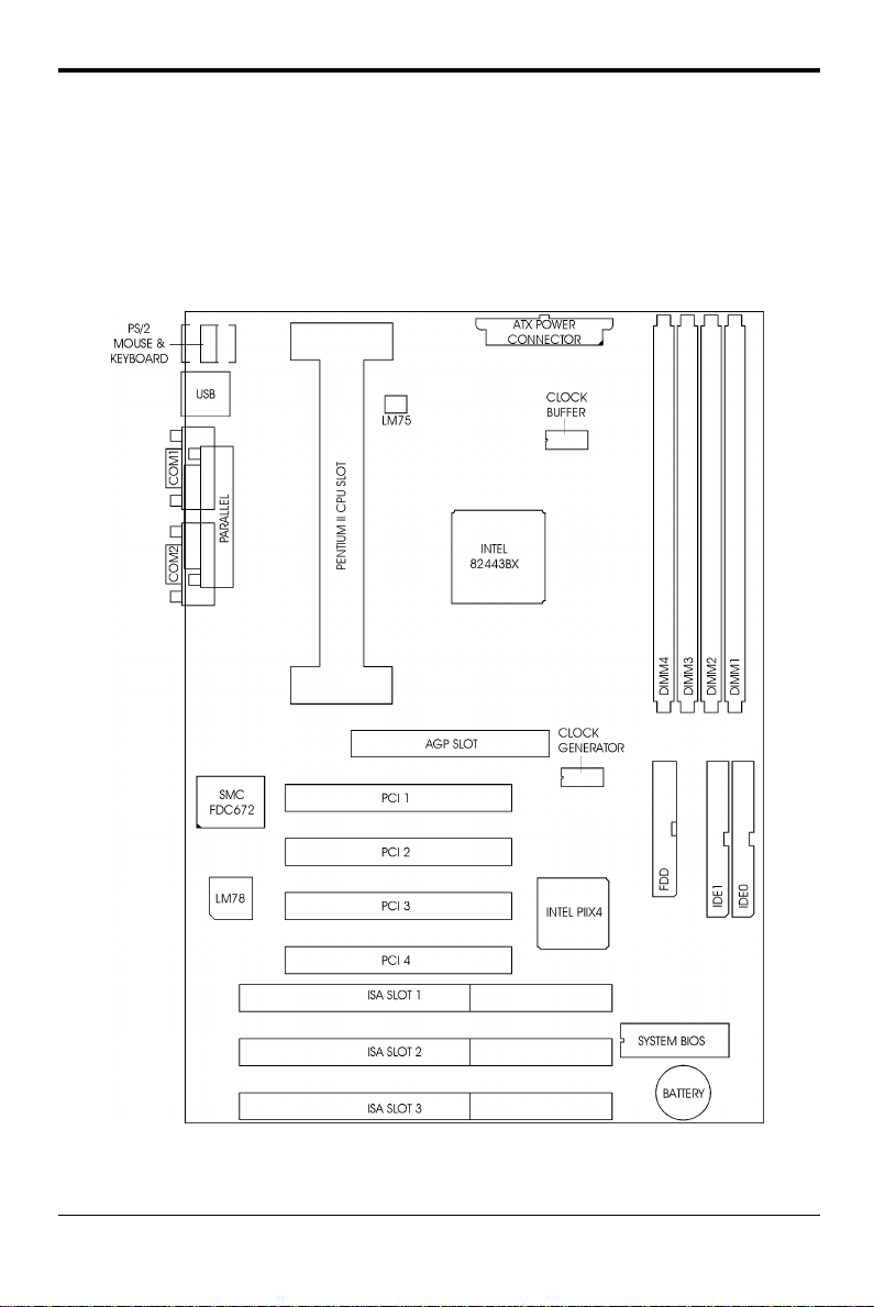
CHAPTER 1 INTRODUCTION
Preface
The motherboard is a 4 layer, ATX form factor high performance PCI/AGP mainboard. It
includes Intel i82440BX system chipset, SMC FDC37M672 Super I/O controller.
Features
Processor
• Intel Celeron, Pentium II/III
• The mainboard can run with following speeds: 233-500MHz
Chipset
• Intel i82443BX (PCI A.G.P. Controller)
• Intel 82371EB (PCI ISA IDE Xcelerator)
• SMC FDC37M672 (Super I/O Controller)
• NS LM75/LM78 (System Voltage & Temperature Monitoring IC)
Main Memory
• Memory configurations up to 1GB SDRAM.
• DIMM socket for 3.3V SDRAM.
• ECC Function ensure data correction and integrity.
Multi I/O
• On board Multi-I/O supports two serial, one parallel ports and floppy drive controller.
• Serial ports are 16550 Fast UART compatible.
• Parallel port has EPP and ECP capabilities.
• PS/2 keyboard and PS/2 mouse connector is provided.
• IrDA supported.
• USB supported.
Accelerated Graphics Port (AGP) Interface
• A.G.P. specification compliant
• A.G.P. 66/133MHz devices supported
PCI IDE
• On board supports PCI Master IDE Controller, two connectors support up to four IDE
devices such as HDD, CD ROM drive and Tape Back-up drives, etc.
• PCI Master IDE controller supports PIO Mode 3 and 4 devices, I/O data transfer rate can be
up to 16.6MB/s.
• Ultra DMA Mode supported. Transfer rate can be up to 33MB/s.
5
Chapter 1
System BIOS
• Award/AMI BIOS (128KB Flash EPROM).
Slots
• One AGP slot
• Four PCI slots (1 shared)
• Three ISA slots(1 shared)
Form Factor
• Full ATX Size (305mm x 217mm) 4 Layer
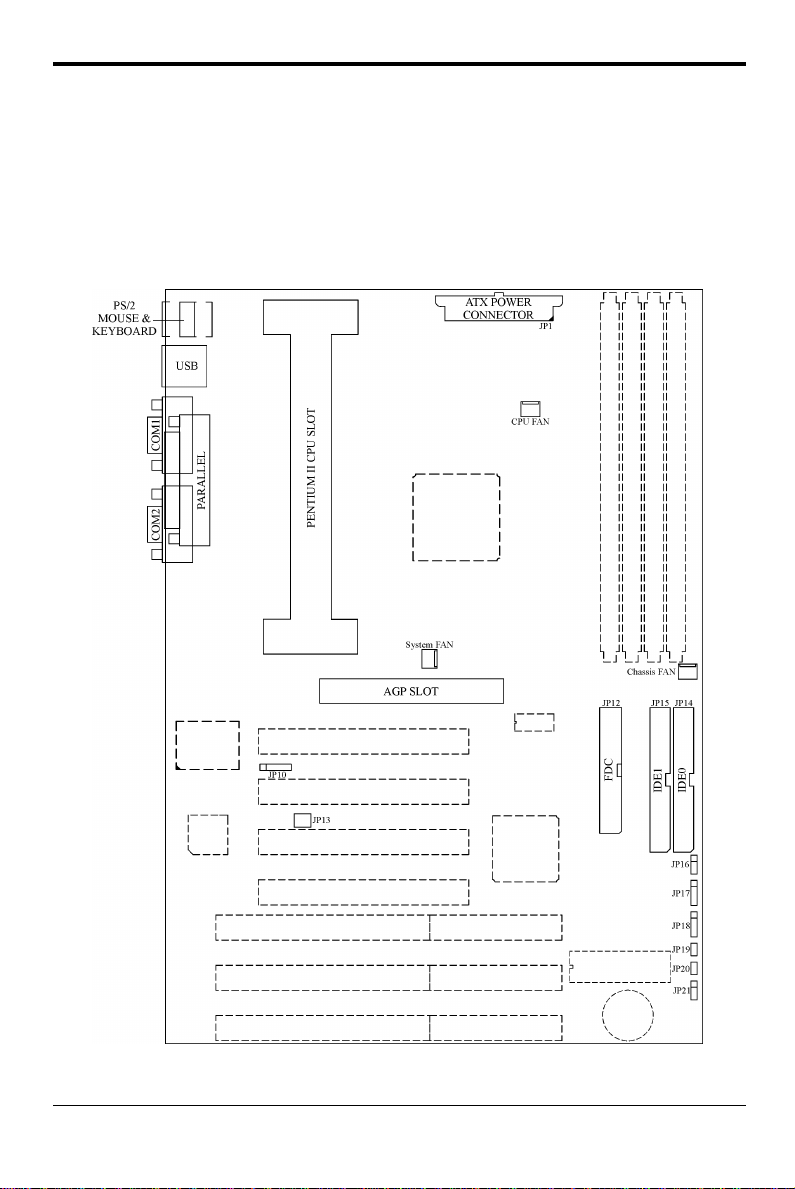
Fig. 1 Key Components of the Mainboard
6
CHAPTER 2 JUMPER SETTINGS
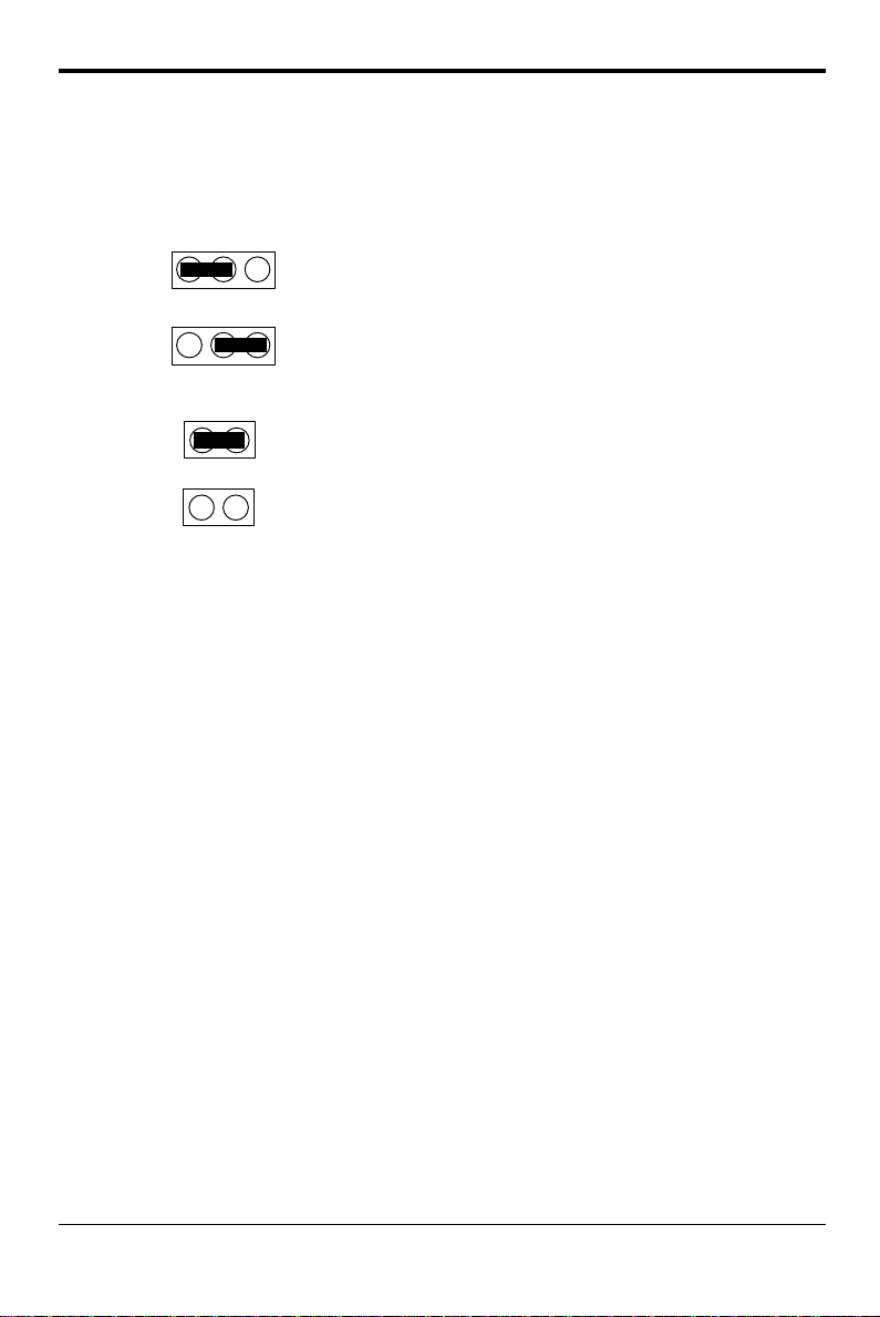
2.1 JUMPERS PRESENTATION
Pins 1 and 2 are shorted with a jumper cap.
1 2 3
Pins 2 and 3 are shorted with a jumper cap.
1 2 3
The jumper is shorted when the jumper cap is placed
over the two pins of the jumper.
The jumper is open when the jumper cap is removed
from jumper.
Jumpers Convention
Different color of jumper caps (mini-jumpers) are used on the board to represent
different usage of the jumpers:
Red: CPU Clock setting
Black: Other
7
Chapter 2
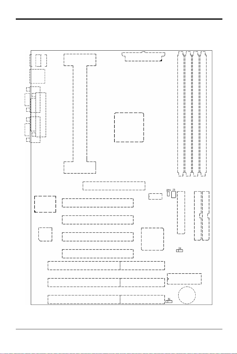
2.2 GRAPHICAL DESCRIPTION OF JUMPER
SETTINGS
Fig. 2 Jumper Location of the mainboard
8
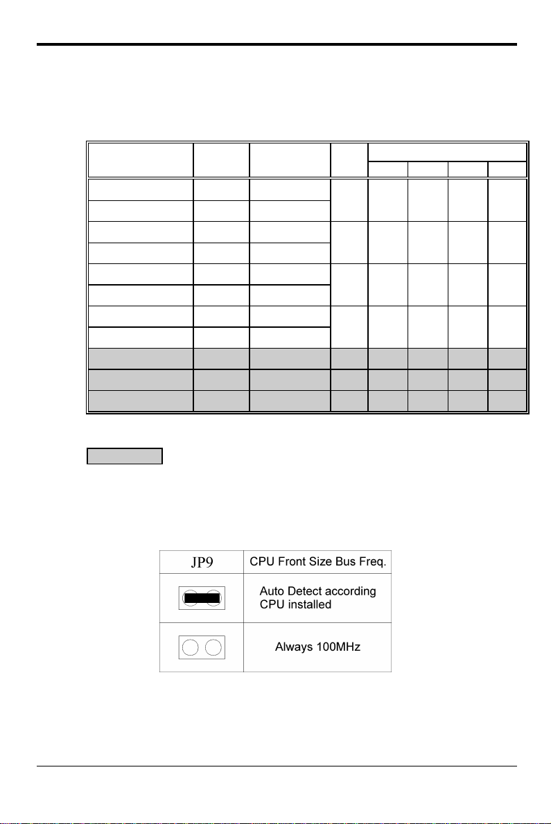
2.3 J3 - CPU CLOCK SPEED
The table below summaries the Processor frequency and settings of each jumper of
the motherboard.
Jumper Settings
CPU Freq.
Pentium II 233MHz 66MHz
Pentium II 350MHz 100MHz
Celeron 266MHz 66MHz
Pentium II 400MHz 100MHz
Celeron 300MHz 66MHz
Pentium II/III 450MHz 100MHz
Celeron 333MHz 66MHz
Pentium II/III 500MHz 100MHz
Celeron 366MHz 66MHz 5.5x close open open open
Celeron 400MHz 66MHz 6.0x open close close close
Celeron 433MHz 66MHz 6.5x open open close close
Table 1: Jumper Setting
Reserve for future support
CPU Front
Size Bus Freq.
Ratio
3.5x close open open close
4.0x close close close open
4.5x close open close open
5.0x close close open open
Rating Setting (J3)
1-2 3-4 5-6 7-8
2.4 JP9 – CPU FRONT SIZE BUS FREQUENCY
SETTING
Table 2: CPU Front Size Bus Frequency Setting
9
Chapter 2
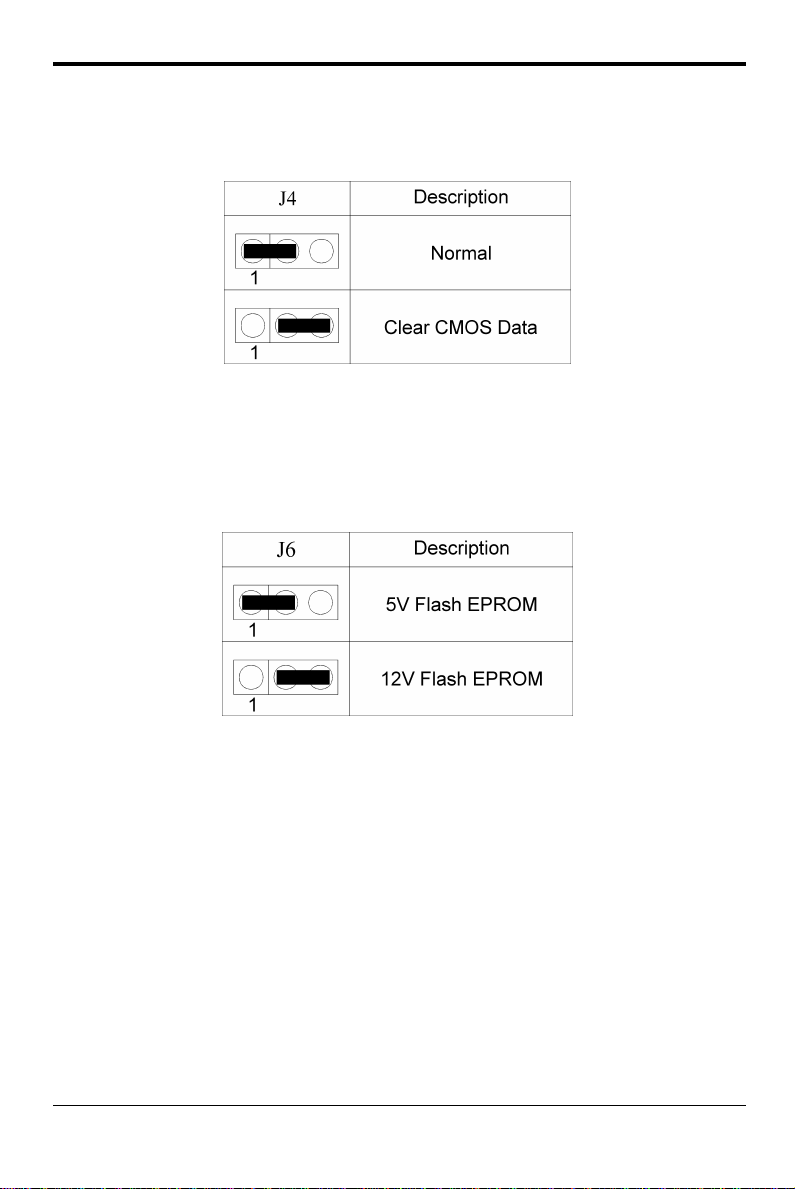
2.5 J4 - CLEAR CMOS DATA
J4 is used to clear the content of the CMOS Data in the RTC (build in PIIX4 chip).
Table 3: Clear CMOS Data
2.6 J6 - VOLTAGE SELECTION FOR SYSTEM ROM
J6 is used to select the operation voltage of the system ROM.
10
Table 4: Voltage Selection for System ROM
Jumper Settings
2.7 MEMORY CONFIGUARTION
When 100MHz Front Size Bus Processor is used. SDRAM DIMMs with PC/100
specification and Serial Presence Defect (SPD) data structure are required. The
mainboard lets user upgrade system memory via DIMM sockets on the mainboard.
On board memory is located in eight banks: Row 0 - 7. Four DIMM sockets are
provided for 3.3V Synchronous DRAM. Table 5 provides the typical memory
configurations supported by the mainboard.
Rows 0/1 (DIMM1) Rows 2/3 (DIMM2) Rows 4/5 (DIMM3) Rows 6/7 (DIMM4)
Installed None None None
None Installed None None
None None Installed None
None None None Installed
Installed Installed None None
Installed None Installed None
Installed None None Installed
None Installed Installed None
None Installed None Installed
None None Installed Installed
Installed Installed Installed None
Installed Installed None Installed
Installed None Installed Installed
None Installed Installed Installed
Installed Installed Installed Installed
Table 5
The maximum memory size is up to 1GB. The size of each DIMM can be 8MB,
16MB, 32MB, 64MB, 128MB or 256MB.
11
CHAPTER 3 CONNECTOR
CONFIGURATION
Once the mainboard has been fastened into system case, the next step is to connect the internal
cables. The internal cables are wire leads with plastic female connectors that attach to the
connectors. The mainboard connectors have varying numbers of pins and are the points of
contact between the mainboard and other parts of the computer.
12
Fig 3 Connector Location
Connector Configuration
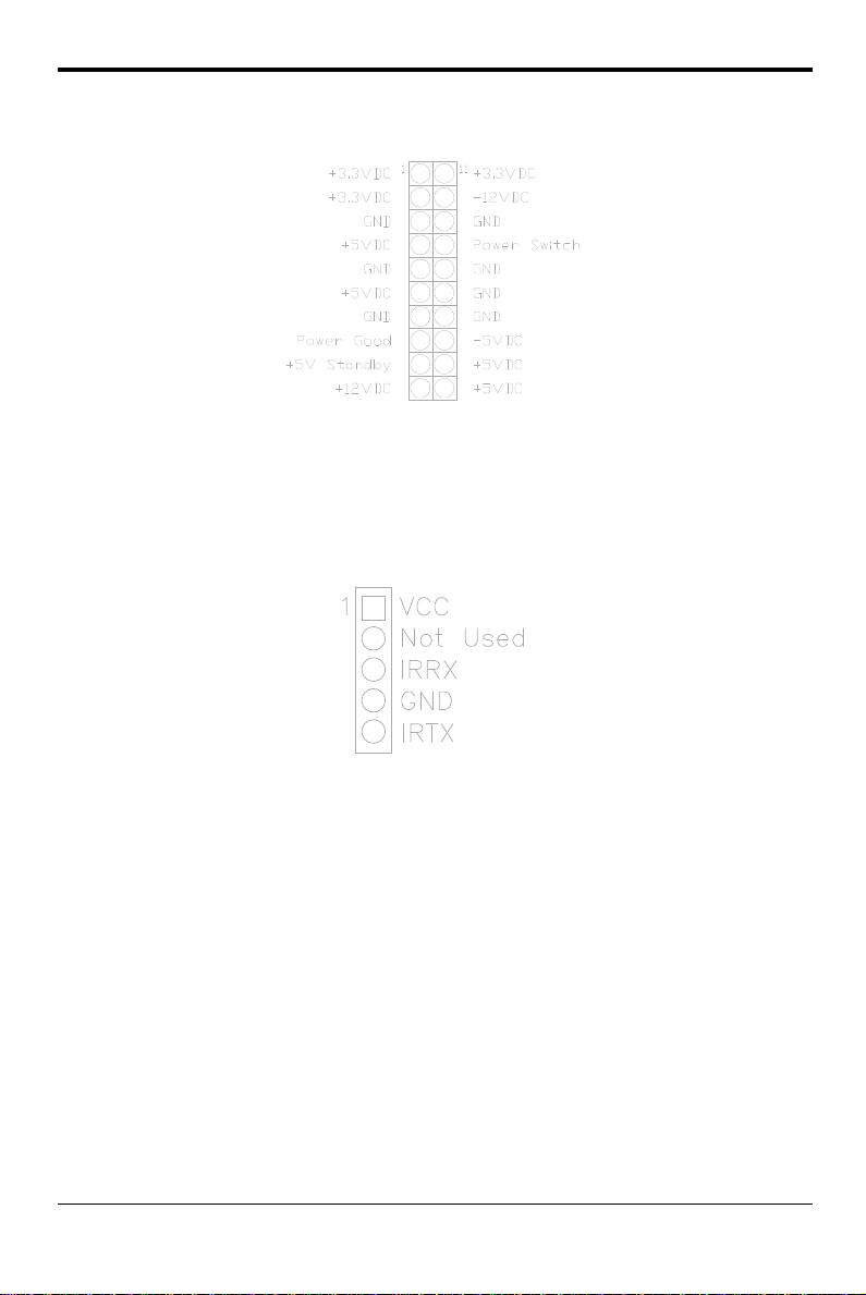
3.1 JP1 - ATX POWER SUPPLY CONNECTOR
Fig. 4 ATX Power Supply Connector
3.2 JP10 - IrDA CONNECTOR
JP10 is an IrDA connector that uses UART2 as interface of IrDA Infrared and HP
SIR.
Fig. 5 IrDA Connector
3.3 JP12 - FLOPPY DRIVE CONTROLLER
This connector supports the floppy drive ribbon cable. After connecting the single
end to the board, connect the two plugs on the other end to the floppy drive.
13
 Loading...