

DTK PRM-0031I User Manual


PRM-00311
High Performance
Pentium Pro PCl Mainboard
User's Guide
Edition 1.11
© 1996 DTK Computer, Inc.

TRADEMARKS
Windows, MS-DOS, and MS Word are trademarks
of
Microsoft Corporation.
Novell, Netware are trademarks
of
Novell, Inc.
Lotus, 1-2-3, and Symphony are trademarks
of
Lotus Development Corporation.
PC, AT, PC-DOS, OS/2 and Presentation Manager are trademarks
of
ffiM
Corporation.
UNIX is the trademark
of
AT&T.
Intel i82440FX and Pentium Pro are registered trademark
of
Intel Corp.
All other brand and product names are trademarks or registered trademarks
of
their
respective companies.
The
information presented in this publication has been carefully checked for
reliability; however, no responsibility is assumed for inaccuracies, whereas,
specification is subjected to change without notice.
ii
iii
CONTENTS
CHAPTER 4 AMI
WINBIOS
SETUP
25
4.1 MOUSE SUPPORT
25
4.2 POINT
& CLICK INTERFACE
25
CHAPTERl
INTRODUCTION
1
4.3 USING KEYBOARD WITH WinBIOS SETUP 26
1.1
GENERAL SPECIFICATION
1
4.4 STARTING WinBIOS SETUP 27
l.2
MAINBOARD COMPONENTS
4
4.5 WinBIOS SETUP MAIN MENU 27
4.6 SETUP 28
CHAPTER 2 MEMORY
CONFIGURATION
5
4.6.1 STANDARD SETUP
29
2.1 SYSTEM MEMORY
5
4.6.2 ADVANCED SETUP
31
4.6.3 CHIPSET SETUP 36
CHAPTER 3 JUMPER
SETTINGS
AND
CONNECTORS
9
4.6.4 POWER MANAGEMENT SETUP
38
3.1 SETTING THE JUMPERS
9
4.6.5
PCIIPnP SETUP
41
3.2
CONNECTION
tHE MOTHERBOARD
11
4.6.6 PERIPHERAL SETUP
44
3.2.1 JUMPER PRESENTATION
11
4.7 SECURITY
47
3.2.2 JUMPER CONVENTION OF THE MOTHERBOARD
11
4.7.1
WINBIOS PASSWORD SUPPORT
47
3.2
.3
CONNECTOR LOCATIONS
12
4.7.2 CHANGING A PASSWORD 48
3.3
CONNECTORS
13
4.7.3 ANTI-VIRUS
49
3.3. 1
120 - POWER SUPPLY CONNECTOR
13
4.8 UTILITY
50
3.3.2
15
- IrDA CONNECTOR
14
4.9
DEFAULT
51
3.3.3
14
- KEYLOCK CONNECTOR
14
4.9.1 ORIGINAL
52
3.3.4
12
- TURBO LED CONNECTOR
15
4.9.2 OPTIMAL
52
3.3.5
17
- SPEAKER CONNECTOR
15
4.9.3 FAIL-SAFE
52
3.3.6
16
- HDD LED CONNECTOR
16
3.3.7
13
- RESET SWITCH CONNECTOR
16
CHAPTER 5 WINBIOS
POWER-ON
SELF
TEST
53
3.3.8 118 - KEYBOARD CONNECTOR
17
5.1
BEEP
CODES
54
3.3.9 I/O CONNECTORS
17
5.2
TROUBLESHOOTING SYSTEM PROBLEMS
55
3.3.
10
117 - PS/2 STYLE KEYBOARD CONNECTOR 5
.3
WinBIOS DISPLAYED ERROR MESSAGES
56
(OPTIONAL)
18
5.4
ISA NMI HANDLER MESSAGES
60
3.3.
11
118 - PS/2 STYLE MOUSE CONNECTOR (OPTIONAL)
18
3.3.
12
JPl
- SMI SWITCH
19
3.3.
13
JP3 - FACTORY TESTING JUMPER
19
3.3.14 112 -
USBO
CONNECTOR 20
3.4.
15
113
- USBI CONNECTOR 20
3.4
GRAPHICAL DESCRIPTIONS OF JUMPER SETTINGS
21
3.4.1 CPU SPEED 22
Introduction
1
CHAPTER!
INTRODUCTION
The
motherboard is a 4-layer, full baby AT size high-performance mainboard.
It
includes Intel i82440FX system chipset, NS PC87306 Super
110
controller.
1.1 GENERAL SPECIFICATION
Processor
• Intel Pentium Pro series.
•
The
mainboard can run with following speeds:
150, 166, 180 and 200 MHz
Chipset
• Intel 82441FX (pCI and Memory Controller)
• Intel 82442FX (Data Bus Xcelerator)
• Intel 82371SB (pCI ISA IDE Xcelerator)
• NS PC87306 (Super
110
Controller)
Main
Memory
• Memory configurations from up to 384MB are possible using
combination
of
256K*36 to 16MB*36 SIMM module. (32Bits non-parity
72-pin SIMM Module also available).
• Support both Fast Page Mode and Extended Data Output (EDO) Mode
DRAM Modules.
• Hidden DRAM Refresh for higher system performance.
• ECC (Error Checking and Correction) support
(Need SIMM module with
parity).
2
Chapter 1
Multi
110
• On board Multi-I/O supports
two
serial, one parallel ports and floppy
drive controller.
• Serial ports are 16550 Fast UART compatible.
• Parallel port has EPP and ECP capabilities.
• IrD A supported.
• USB supported.
PCIIDE
• On board supports PCI Master IDE Controller, two connectors support up
to four IDE devices such as HDD,
CD
ROM drive and Tape Back-up
drives, etc.
• PCI Master IDE controller supports PIO Mode 3 and
4 devices, I/O data
transfer rate can be up to 17Mb/s. DMA mode transfer rate can be up to
22Mb/s.
System
BIOS
• AMI BIOS (128KB Flash EPROM).
Slots
• Five PCI slots
(1
shared)
• Three ISA slots
(1
shared)
Introduction 3
~~~~~----------------------------------------------
Board
.4
Layer
Form Factor
• Full Baby AT Size (220 x 330mm)
4
1.2
16-
81l
-
( XPANSI
~
SLOTt
Chapter 1
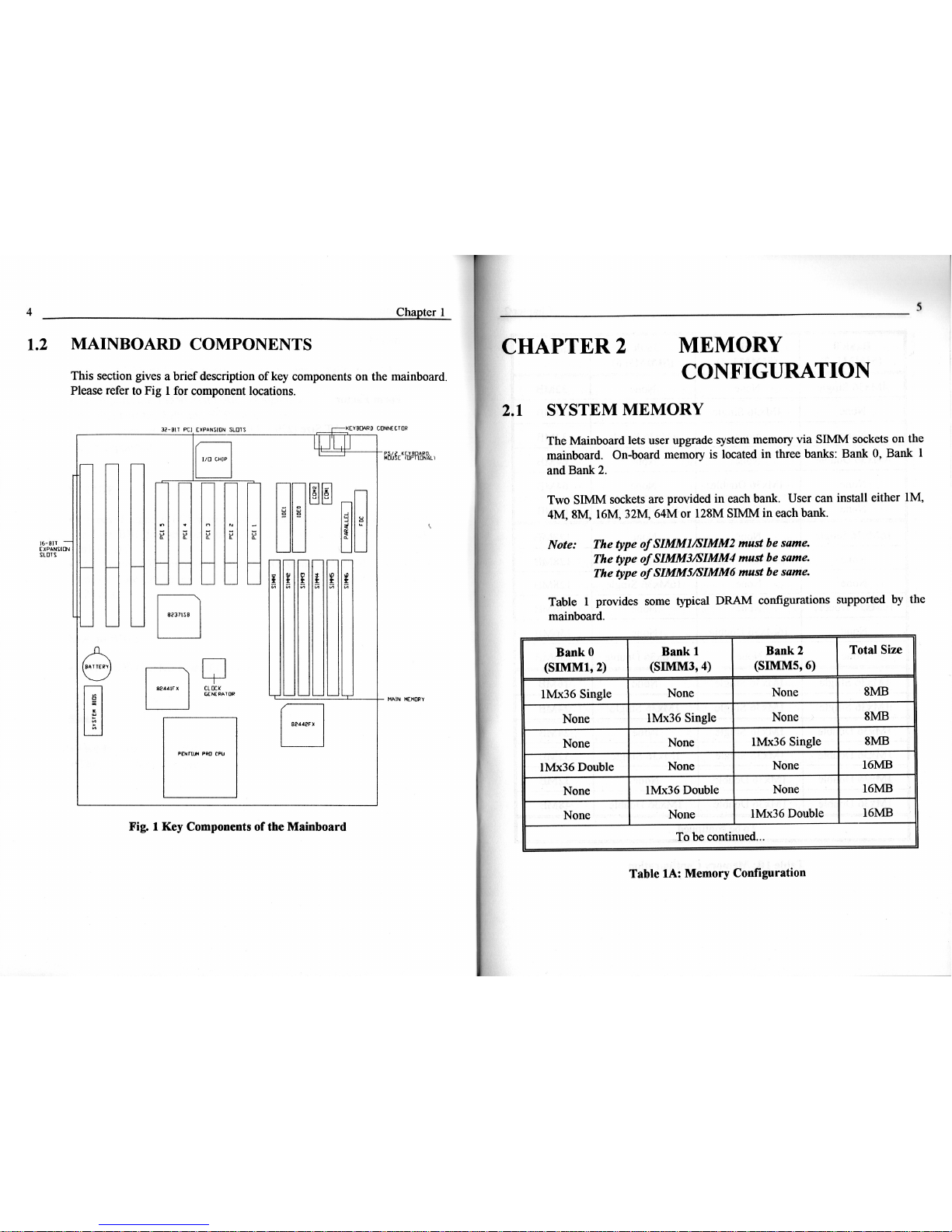
MAINBOARD COMPONENTS
This section gives a brief description
of
key components on the mainboard.
Please refer to Fig 1 for component locations.
32-
BIT
PC)
(XPANSIDN
SLOTS
-.r::::...1<[YBClAF?D
C
(]NN(CTO~
El
W
~BG~EKfb',l'Hm.~ll
~
~
~
~~rnoo
...
.
...
'"
-
Ii
~~
~
~
u
~
~
Q.
I--
I--
l-
I-
I--
I--
I-- I--
r-r-r-r-r-r-
'--
'--
'--
l.......
'--
I
~
~
i
~
f
0;
0;
0;
;;;
0;
L.-
'--
L.-
a
to
B
0
rn
ClOC.
C,CN(rlAl[JQ
c,..'-'-'-'-c,-
MAJN
H(MDRY
EJ
p[Nru
....
pit[)
CPU
Fig. 1 Key Components
of
the
Mainboard
_____________________________________________________
5
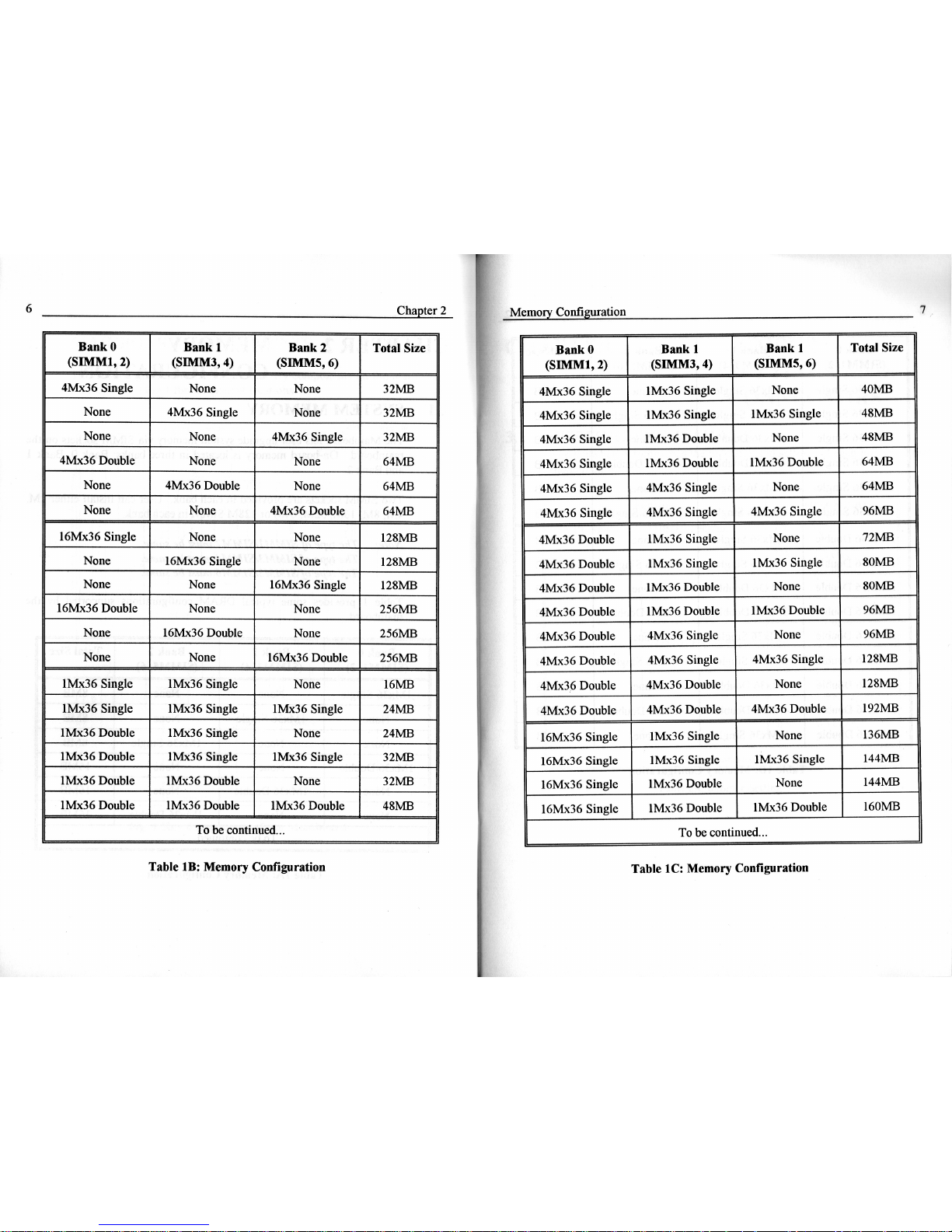
CHAPTER 2 MEMORY
CONFIGURATION
2.1 SYSTEM
MEMORY
The Mainboard lets user upgrade system memory via SIMM sockets on the
mainboard. On-board memory
is
located in three banks: Bank
0,
Bank 1
and Bank
2.
Two SIMM sockets are provided in each bank. User can install either 1M,
4M,8M
, 16M, 32M, 64M or 128M SIMM in each bank .
Note: The type
of
SIMMllSIMM2 must be same.
The type
of
SIMM31SIMM4 must be same.
The type
of
SIMM51SIMM6 must be same.
Table 1 provides some typical DRAM configurations supported
by
the
mainboard.
BankO
Bank
1
Bank
2
Total Size
(SIMMl,2)
(SIMM3,4)
(SIMM5,6)
IMx36 Single None None 8MB
None
IMx36 Single None 8MB
None
None IMx36 Single 8MB
IMx36 Double None None 16MB
None
IMx36 Double None 16MB
None None IMx36 Double
16MB
To
be
continued ...
Table
lA:
Memory Configuration
6
Chapter 2
~M~e~m~o~ryLC~onfi~l~~a~b~'o~n
_____________________________________
7
BankO
Bank
I
Bank
2
Total Size
BankO
Bank
I
Bank
I
Total Size
(SIMMl,2)
(SIMM3,4)
(SIMMS, 6)
(SIMMI,2)
(SIMM3,4)
(SIMMS, 6)
4Mx36 Single None None 32MB
4Mx36 Single
IMx36 Single
None
40MB
None 4Mx36 Single None
32MB
4Mx36 Single
IMx36 Single
IMx36 Single
48MB
None
None
4Mx36 Single 32MB
4Mx36 Single
IMx36 Double
None
48MB
4Mx36 Double None None 64MB
4Mx36 Single
IMx36 Double
IMx36 Double
64MB
None 4Mx36 Double None 64MB
4Mx36 Single
4Mx36 Single
None
64MB
None None 4Mx36 Double 64MB
4Mx36 Single
4Mx36 Single
4Mx36 Single
96MB
16Mx36 Single None None
128MB
4Mx36 Double
IMx36 Single
None
72MB
None
16Mx36 Single None
128MB
4Mx36 Double
IMx36 Single
IMx36 Single
80MB
None None 16Mx36 Single
128MB
4Mx36 Double
IMx36 Double
None
80MB
16Mx36 Double None None 256MB
4Mx36 Double
IMx36 Double
IMx36 Double
96MB
None
16Mx36 Double None 256MB
4Mx36 Double
4Mx36 Single
None
96MB
None
None
16Mx36 Double 256MB
4Mx36 Double
4Mx36 Single
4Mx36 Single
128MB
IMx36 Single
IMx36 Single None 16MB
4Mx3,6 Double
4Mx36 Double
None
128MB
IMx36 Single
IMx36 Single
IMx36 Single 24MB
4Mx36 Double
4Mx36 Double
4Mx36 Double
192MB
IMx36 Double
IMx36 Single None
24MB
16Mx36 Single
1 Mx36 Single
None
136MB
IMx36 Double
IMx36 Single IMx36 Single 32MB
16Mx36 Single
IMx36 Single
IMx36 Single
144MB
IMx36 Double
IMx36 Double None
32MB
16Mx36 Single
IMx36 Double
None
144MB
IMx36 Double
IMx36 Double IMx36 Double
48MB
16Mx36 Single
IMx36 Double
IMx36 Double
160MB
To be continued ...
To
be
continued ...
Table
IB:
Memory
Configuration
Table
IC:
Memory
Configuration
8
Chapter 2
BankO Bank 1 Bank 2
Total Size
(SIMMl,2)
(SIMM3,4) (SIMM5,6)
16Mx36 Single
4Mx36 Single None 160MB
16Mx36 Single
4Mx36 Single 4Mx36 Single 192MB
16Mx36 Single
4Mx36 Double None
192MB
16Mx36 Single
4Mx36 Double 4Mx36 Double
256MB
16Mx36 Single 16Mx36 Single None
256MB
l6Mx36 Single l6Mx36 Single l6Mx36 Single 384MB
16Mx36 Double lMx36 Single None 264MB
16Mx36 Double 1Mx36 Single 1Mx36 Single
272MB
16Mx36 Double IMx36 Double None
272MB
16Mx36 Double
1Mx36 Double 1Mx36 Double 288MB
16Mx36 Double 4Mx36 Single None
288MB
16Mx36 Double 4Mx36 Single 4Mx36 Single
320MB
16Mx36 Double 4Mx36 Double
None 320MB
16Mx36 Double 4Mx36 Double 4Mx36 Double 384MB
16Mx36 Double 16Mx36 Single None 384MB
Table ID: Memory Configuration
CHAPTER
3
JUMPER
SETTINGS AND
CONNECTORS
3.1
SETTING
THE
JUMPERS
9
The table below summaries the functions and settings
of
each jumper
of
the
motherboard.
Function
Jumper
Settings
CPU
Speed
150MHz Pentium Pro
JP6:
open
Selection
JP7:
close
JP8:
1-8 close,
2-7 open,
3-6 close,
4-5 close
JP9:
1-3
close,
2-4 close
166MHz Pentium Pro
JP6:
close
JP7:
open
JP8:
1-8 open,
2-7 close,
3-6 close,
4-5 close
JP9:
1-3
close,
2-4 open
To be continued
..
.
Table 2A:
Jumper
Setting
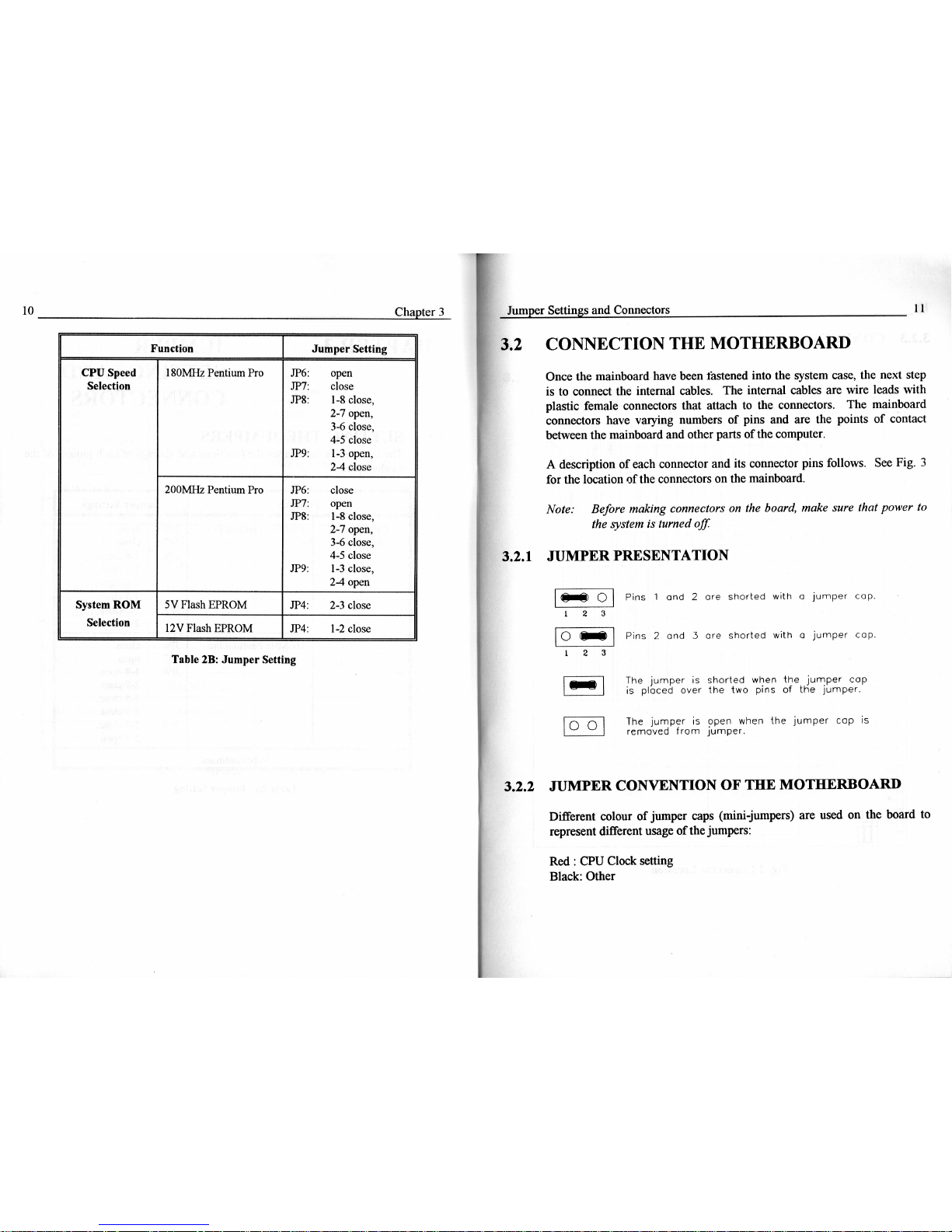
lO
____________________________________________
~C~h~ap~t~er~3~
Function
Jumper
Setting
CPU Speed
180MHz Pentium Pro JP6: open
Selection
JP7: close
JP8:
1-8
close,
2-7 open,
3-6 close,
4-5 close
JP9:
1-3
open,
2-4 close
200MHz Pentium Pro
JP6: close
JP7:
open
JP8:
1-8
close,
2-7 open,
3-6 close,
4-5 close
JP9:
1-3
close,
2-4 open
System
ROM
5V Flash EPROM
JP4:
2-3 close
Selection
12V Flash EPROM
JP4:
1-2
close
Table 2B:
Jumper
Setting
Jumper Settings and Connectors
II
3.2 CONNECTION THE MOTHERBOARD
Once the mainboard have been tastened into the system case, the next step
is to connect the internal cables. The internal cables are wire leads with
plastic female connectors that attach
to
the connectors. The mainboard
connectors have varying numbers
of
pins and are the points
of
contact
between the mainboard and other parts
of
the computer.
A description
of
each connector and its connector pins follows. See Fig . 3
for the location
of
the connectors on the mainboard.
Note: Before making connectors
on
the
board, make sure that power
to
the system is turned off.
3.2.1
JUMPER
PRESENTATION
1
~
0 I Pins
land 2 are
shorted
with a jump
er cop.
2 3
10 _I
Pins 2
and 3 ar
e sho
rted
with a jumper cop.
2 3
The jumper
is shorted when the
jumpe
r c
op
is
placed ov
er the two
pins
of the
jump
er.
The j
umper
is open
when
the
jumper
cop
is
remo
ved
from jumper
.
3.2.2
JUMPER
CONVENTION
OF
THE
MOTHERBOARD
Different colour
of
jumper caps (mini-jumpers) are used on the board to
represent different usage
of
the jumpers:
Red:
CPU Clock setting
Black: Other

12
______________________________________________
C~ha~p~te~r~3~
3.2.3
CONNECTOR
LOCATIONS
1---1
I I
I I
I I
I I
I I
I I
I I
I I
I I
I I
'-_oJ
1---1
I I
I I
I I
I I
I I
I I
I I
I I
I I
I I
'-_oJ
it
~
"
r \
I \
I I
\ J
'--"
r--,
I I
I \
I I
I I
I I
I I
I I
I I
L..
__
.J
r-.,
I
I
I
I
I
I
I
I
I
I
I
I
I
I
I
I
I
I
t---t
I I
I I
I I
I I
I I
I I
I I
I I
I I
I I
'-_oJ
(,-----l
I I
I I
I I
I I
L
_____
...l
r-l
r-l r-l
I
I
I
I
I
I
I
I
I
I
I
I
I
_J
I I I
I I I
I I I I
L_J L_J
L_J
r-----""'-
I
~
I I
I I
I I
I I
I I
L
______
-1
r------...
I
~
I I
I I
I I
I I
I I
L
______
...J
r------------..,
I
I
I
I
I
I
I
I
I
I
I
I
I
L
___________
_
JB
J9
JlD ..ttl
r-l
~OO
I
I
I
I
W
..
I
t.J
I
B
B
I
ffi
I
I
I
I
I
I
L_J
I I
I I
2
I I
!i
~
:I
~
L_J
~ ~
i!i
~
~
..
,..------,
( I
I I
I I
I I
I I
I I
L
______
...J
Fig. 2
Connector
Location
J15
J14
~
H
"'-
~
~
Jumper Settings
and
Connectors
13
3.3
CONNECTORS
3.3.1
J20 -POWER
SUPPLY
CONNECTOR
The
power supply connector has two six-pin male header connectors.
Plug
the dual connectors from the power directly onto the board connector.
Pin
Description
1
Power. Good (Orange)
2
+5 VDC (Red)
3
+
12
VDC (Yellow)
4
-12 VDC (Blue)
5 Ground (Black)
6
Ground (Black)
7
Ground (Black)
8 Ground (Black)
9
-5 VDC (White)
10
+5 VDC (Red)
11
+5 VDC (Red)
12
+5 VDC (Red)
Table
3:
J20
-
Power
Supply
Connector
 Loading...