

DTC DTC-510B, DTC-520B, DTC-535BK User Manual
Data
Technology
Corporation
DTC
5008
Series
DISK CONTROLLERS
USER'S MANUAL
DATA
TECBIIlOLOGY
CORPORATION
DTC
588B
SERIES
DISK COIiTROLLERS
USER'S
MANUAL
DTC
part
number
89-88181.
Revision
88
Data
Technology
Corporation
Main
Office
2775
Northwestern
Parkway
Santa
Clara,
California
95851
(488)496
8434
Eastern
Region
Sales
Office
16
Wiggins
Avenue
Bedford,
HA
81738
(617)
275-4844

PREFACE
warranty
Data
Technology
corporation
(DTC)
maintains
a
complete
Repair
Department
for
the
sole
purpose
of
providing
efficient,
reliable
service.
All
DTC
products
are
warranted
against
defects
in
material
and
workmanship.
The
period
of
coverage
and
other
warranty
details
are
clearly
specified
in
the
DTC
purchase
agreement.
Check
this
agreement
for
exact
warranty
details.
Accuracy
All
information
in
this
manual
is
based
on
the
latest
product
information
available
at
the
time
of
printing.
DTC
has
reviewed
the
accuracy
of
the
technical
specifications,
but
DTC
cannot
be
held
responsible
for
any
omissions
or
errors
that
may
appear
in
this
manual.
Change
Information
The
DTC
product
line
is
constantly
being
reviewed
and
improvements
are
implemented
when
appropriate.
From
time
to
time
DTC
will
distribute
Field
Change
Orders
and
Technical
Bulletins
to
inform
users
of
enhancements
or
improvements
to
their
products.
Trademarks
LSI-II
is
a
trademark
of
Digital
Equipment
Corporation
VERSAbus
is
a
trademark
of
Motorola
Corporation
SASI
is
a
trademark
of
Shugart
Associates
IBM
Personal
Computer
is
a
trademark
of
International
Business
Machines
Corporation.
Multibus
is
a
trademark
of
Intel
Corporation
Reproduction
Information
in
this
manual
must
not
be
reproduced
by
any
means
without
the
prior
written
approval
of
DTC.
--i--

SECTION
3
3.5.2
3.5.3
3.5.3.1
3.5.3.2
SECTION 4
4.1
4.2
4.2.1
4.2.2
4.2.3
4.2.4
4.2.5
4.3
SECTION 5
5.1
5.2
APPENDIX
A
A.l
A.2
A.3
APPENDIX B
B.l
APPENDIX C
C.l
c.l.l
C.l.2
C.l.3
C.2
APPENIDX D
APPENDIX E
APPENDIX
F
COMMANDS
AND
STATUS
Page
OpCode
01
(Assign
Drive
Type)
(535B
only);
.......••••.
76
Opcode
02
(Set
Drive.
Parameters)
.•..••••.••...•.••...
77
~linchester
Drive
Parameters
.•••••.•••...•..•..••
78-80
Floppy
Drive
Parameters
(520B
only)
•••••••..••....•......•..••.....•
81-83
MAINTENANCE & TROUBLESHOOTING
Overv
iew
.••.•..•••••••....•..•....•....•..•....••...•
84
Class
Code
7
Commands
••..••••..•.••.••••.••••.••..•..
84
OpCode
00
(RAM
Diagnostics)
....•.••....••.••••.••.•..
86
Opcode
01
(Write
ECC
Error)
.••.•..•••..•.•..•.
,
•...••
86
Opcode
02
(Read
ID
Field)
••.••.•..•••.•........•....•
88
OpCode
03
(Perform
Drive
Diagnostics)
.•.•..••..•.....
90
OpCode
06
(Request
Logout)
..••••.••..••.•..••.••..
90-92
LED
Error
Display
.••.•••.••.••.•.••••..••.••.•..•.•.•
93
APPENDICES - INSTALLATION
AND
GENERAL
INFORMATION
Introduction
.........•..•.....•..••......•••.•.•.....
95
Mounting
•••.•....•.•••...••.•..•.••.•........•..••.•.
95
LOGICAL
ADDRESS
Overview
...•••...•..•...........•.••..•.•...•.....•..
96
Calculation
of
Logical
Address
•.••..•••.••....•
,
..
96-97
Determining
Cylinder
Addresses
•.•••.•..•..•..•.......
98
INTERLEAVE
Interleave
•..••••..••..•.......•..••.••.••••...•..•..
99
SECTOR
FORMATS
Winchester
Drive
Sector
Formats
..•.•.••..•..........
102
256
Bytes
per
Sector/33
Sectors
per
Track
•.•..••..•.
102
512
Bytes
per
Sector/18
Sectors
per
Track
....•.....•
103
1,024
Bytes
per
Sector
/9
S,ectors
per
Track
•••.••••.•
103
Floppy
Drive
Format
.•••.•.••...•.•.•.••.••.•••••..•.
103
ALTERNATE
TRACK
USAGE
WITH
DTC
CONTROLLERS
.........
.
104
IMPLEMENTING
OVERLAPPED
SEEKS
ON
DTC
DISK
CONTROLLERS .........................................
105
JUMPER
SETTINGS
FOR
DTC
518B
•....•.•....•..•........
106
--iii--

TABLE
OF
CONTENTS
(continued)
APPENDICES
Page
APPENDIX G
SWITCH SETTINGS
AND
JUMPER CONFIGURATION
FOR
52BB
•••
109
APPENDIX H
SWITCH SETTINGS
AND
JUMPER CONFIGURATIOIil
FOR
535B
•••
112
H-l
Jumper
Settings
for
SA800/80l
.......................
115
H-2
Jumper
Settings
for
SA850/SA85l
.....................
116
H-3
Jumper
Settings
for
TAN
DON
TA848-l/2
...............
116
H-4
Jumper
Settings
for
AMLYN
5850
......................
117
APPENDIX J
SWITCH SETTINGS
AND
JUMPER CONFIGURATION
FOR
535BK
..
118
J-l
DTC-5358K
Factory
Settings
..........................
120
J-2
Switch
Settings
for
KODAK
3.3
.......................
120
LIST
OF
TABLES
TABLE
1-1
Controller
Features
...........................................
2-4
1-2
Specifications
..................................................
4
2-1
Interpretaion
of
Request
.......................................
11
3-1
Summary
of
Class
Code'"
OpCodes
....................
:
........
35-37
3-2
Sense
Byte
Error
Codes
.......•.............................•...
44
3-3
Floppy
Drive
Track
Format
(Byte
5
Class.
Code
6)
............
72-73
4-1
Class
Code
7 Commands
..........................................
85
4-2
LED
Error
Displays
.............................................
94
LIST
OF
ILLUSTRATIONS
FIGURES
2-1
2-2
2-3
2-4
2-5
2-6
2-7
2-8
2-9
2-10
3-1
3-2
3-3
3-4
3-5
3-6
Typical
System
Configuration
............................
,
.......
7
500B
Series
Host
Interface
Signals
and
Pin
Designation.
'"
......
8
Controller
to
Winchester
Drive
Control
Interface
...............
12
Controller
to
Winchester
Drive
Data
Interface
..................
13
520B
Controller
to
Floppy
Disk
Drive
Interface
.................
14
535B
Controller
to
Floppy
Drive
Interface
......................
15
5358
Controller
to
Amlyn
Drive
Interface
.•.....................
16
535BK
Controller
to
KODAK
Disk
Drive
Interface
..............•..
17
Timing
Diagrams
.............•...............................
20-25
Flowcharts
..................................................
26-29
Typical
Command
Discriptor
Block
(CDB)
.........................
32
Test
Drive
Ready
...............................................
38
Recalibrate
Drive
..............................................
39
Request
ECC
Syndrome
.....................•..................•..
40
Request
Sense
..................................................
41
Format
Drive
..............................................••...
46
--iv--
TABLE
OF
CONTENTS
(continued)
LIST
OF
ILLUSTRATIONS
FIGURES
Page
3-7
3-8
3-9
3-10
3-11
3-12
3-l3
3-14
3-15
3-16
4-1
4-2
4-3
B-1
F-l
F-2
G-l
G-2
H-l
H-2
J-l
J-2
Check
Track
Format
..................•..........................
48
Format
Track
.....•.............•..............•................
50
Format
Bad
Track
.•..................•.................•........
52
Read
Block
Command
Flowchart
...................................
55
Write
Block
Command
Flowchart
..................................
58
Seek
•........•.................................................
61
Search
Routine
Flowchart
.......................................
65
Random
Read
Routine
Flowchart
..................................
66
Increment
Sector,
Head,
or
Cylinder
Flowchart
..................
67
Copy
Command
Flowchart
.........................................
70
h'ri
te
ECC
Command
..............................................
87
,
Read
ID
Field
..................................................
89
Drive
Diagnostic
...............................................
91
Physical
versus
Logical
Sector
................•......•....
100-101
DTC
510B
Cable
Connections
....................................
107
DTC
510B
Board
Outline
with
Mounting
Holes
....................
108
DTC
520B
Cable
Connections
............•.......................
110
DTC
520B
Board
Outline
with
Mounting
Holes
....................
111
DTC
535B
Cable
Connections
....................................
1Ll'
DTC
535B
Board
Outline
with
Mounting
Holes
....................
11~
DTC
535BK
Cable
Connections
.....•...•.........................
121
DTC
535BK
Board
Outline
with
Mounting
Holes
...•...............
122
--v--
SECTION 1
1.1
Scope
of
Guide
This
guide,
for
Data
Technology
Corporation's
500B
Series
Disk
Drive
Controllers,
provides:
Equipment
Information
and
Specifications
Interface
and
Configuration
Information
Command
and
Programming
Information
Installation
and
Testing
Instructions
Maintenance
and
Troubleshooting
Hints
This
guide
is
intended
to
satisfy
the
information
requirements
of
OEM
Engineers;
Engineering
and
Production
Technicians;
Personal
Computer
Enthusiasts;
and
others
with
a
need
to
know
about
these
disk
Controllers.
1.2
Overview
of
Equipment
The
DTC-5l0B
is
designed
to
control
two
industry
standard
ST506/406
or
compatible
5.25
Winchester
Disk
Drives.
The
DTC-520B
is
designed
to
control
a maximum
of
four
disk
drives.
It
supports
up
to
two
ST506/406
or
compatible
5.25
inch
Winchester
Disk
Drives
plus
two
industry
standard
SA4XX,
or
equivalent,
(48
or
96TPI)
Floppy
Disk
drives.
The
DTC-535B
is
designed
to
control
a maximum
of
four
drives
in
any
combination
of
up
to
two
industry
standard
5.25
inch
Winchester
Disk
Drives,
and
any
combination
of
two
industry
standard
SA8XX
type
interface
8
inch
Floppy
Disk
Drives.
Alternately,
it
can
be
strapped
tor
a
combination
of
two
hard
disk
drives
and
two
AMLYN
5850
drives
or
one
SA8XX
and
one
AMLYN
5850.
The
DTC-535BK
is
designed
to
control
a maximum
of
four
drives
in
any
combination
of
up
to
two
industry
standard
ST506
5.25
inch
Winchester
Disk
Drives,
or
equivalent,
or
up
to
four
5.25
inch
KODAK
3.3
Floppy
Disk
Drives.
Currently
supported
disk
drives
are
produced
by:
KODAK
IMI
SEAGATE
COGITO
BASF
MPI
SHUGART
QUANTUM
Cii-HB
OPE
TAN
DON
MICROPOLIS
CMI
RODIME
TI
TULIN
FUJITSU
MINI SCRIBE MICROSCIENCE
MAXTOR
The
interface
to
the
!lost
Computer
is
via
the
industry
standard
SASI
bus
and
is
easily
accomplished
by a standard
DTC
Host
Adapter.
DTC
is
a
major
supplier
of
SASI
compatible
Host
Adapters
for
most
computer
system
buses.
--1--
1.2
OVerview
of
Equipment
(continued)
Contact
your
DTC
sales
representative
for
information
on
available
Host
Adapters.
Proprietary
LSI
Circuits,
based
on
DTC's
field-proven
design,
allow
for
enhanced
performance,
small
size
and
economy.
Reliability
and
maintainability
have
been
proven
by
statistical
information
from
field
installation.
The
Mean
Time
between
Failures
(MTBF)
for
these
Controllers
is
20,000
hours.
The
Mean
Time
to
Repair
(MTTR)
is
0.1
hour.
Features
found
in
a
DTC-500B
Series
Controller
are
given
in
Table
1-1.
AUTOMATIC SEEK
VERIFY
MULTIPLE
BLOCK
TRANSFERS
AUTOMATIC HEAD
and
CYLIII1DER
SWITCHIHG
PARITY
SELECTIOH
PROGRAMMABLE
SECTOR
IBTERLEAVIHG
BARD
DISK
SECTOR
SIZE
·PROGRAMMABLE
FLOPPY
TRACK
FORMAT
TABLE
1-1
Controller
Features
A
seek
command
is
implied
in
every
data
transfer
command
(READ, WRITE,
CHECK
TRACK
FORMAT,
etc.).
If
the
heads
are
not
positioned
over
the
correct
cylinder,
a
seek
is
initiated,
and
a
cylinder
verification
is
performed
after
the
seek
completes.
Allows
more
than
one
block
to
be
transferred
with
one
command.
~ilien
the
end
of
a
track
is
reached
(during
a
multi-block
data
transfer)
the
Controller
switches
heads
to
the
next
track.
lilien
the
end
of
a
cylinder
is
reached,
the
Controller
seeks
to
the
next
cylinder,
selects
head
0
and
resumes
transfer.
Odd
parity
is
generated
within
the
Controller
for
all
information
put
on
the
I/O
bus.
~fuen
parity
is
enabled
(by
jumper
selection)
all
bad
parity
information
is
flagged.
Up
to
a
16
way
programmable
interleave
is
provided.
Selectable
Winchester
Sector
size
of
256
bytes
(33
Sectors),
512
bytes(18
sectors),
or
1,024
bytes
(9
Sectors).
The
type
of
track
format
on
the
floppy
media
that
is
going
to
be
used
can
be
passed
to
the
Controller
through
software.
--2--
MEDIA
ASSIGNMENT
FUNCTION
HOST
INTERFACE
PROTOCOL
LOGICAL
to
PHYSICAL
DRIVE
CORRELATION
PROGRAMMABLE
DISK
DRIVE
PARAMETERS
DOUBLE
STEP
FUNCTION
CONTROLLER
10
SELECTABLE
ON
BOARD
SECTOR
BUFFER
ALTERNATE
TRACK
ADDRESSING
DATA
ERROR
SENSING
and
CORRECTION
TABLE
1-1
Contro11er
Features
(continued)
This
function
allows
the
user
to
read
conventional
48
tpi
or
96.tpi
diskettes
on
KODAK
3.3
disk
drive.
A
bi-directional
(SASI)
bus
between
the
Controller
and
Host
provides
a
simple.and
efficient
communication
path.
A
high
level
command
set
permits
effective
con~and
initiation.
Logical
unit
numbers
(LUN's)
are
independent
of
physical
port
numbers.
All
accesses
specify
LUN's
The
disk
drive
parameters
are
passed
to
the
Controller
from
the
Host
(as
data)
to
define
the
drive's
characteristics.
Standard
firmware
supports
up
to 8 heads.
Up
to
1024
cylinders
are
supported.
Optional
firmware
on
some
Controllers
support
up
to
16
heads.
Allows
the
user
to
Read/Hrite
48
TPI
diskettes
on a 96
TPI
Floppy
Drive.
A
jumper
is
provided
to
specify
the
Controller
ID
number
on
the
5l0B
and
520B.
The
535B
and
535BK
use
switches
to
specify
the
Controller
ID
number.
A
sector
buffer
is
provided
on
the
Controller
to
eliminate
the
possibility
of
data
overruns
during
a
data
transfer.
The
Host
can
assign
an
alternate
track
for
a
defective
track.
(Subsequent
accesses
to
the
defective
track
will
cause
the
Controller
to
transfer
data
from
the
alternate
track
address).
The
maximum
number
of
alternate
track
addresses
is
half
the
total
number
of
tracks
on
the
disk.
If
a
data
error
is
detected
during
a
disk
data
transfer,
the
Controller
indicates
whether
or
not
it
is
correctable.
If
correctable,
either
a
pointer
and
mask
can
be
requested
by
the
Host
for
applying
the
correction
or
the
error
can
be
automatically
corrected.
--3--
FAULT
DETECTION
ERROR
INDICATORS
1.3
Specifications
TABLE
1-1
Controller
Features
(continued)
In
the
5008
series
Controller,
two
classes
of
faults
are
flagged
to
improve
error
handling:
*
Controller
faults
*
Disk
faults
Eight
LED
indicators
are
installed
to
aid
in
the
analysis
of
errors.
Specifications
are
given
on
Table
1-2.
Environmental
Parameters
Ambient
Temperature
Relative
Humidity
(At
40
degrees
F
wet
bulb
temperature
and
no
condensaQJon)
Altitude
Physical
Dimensions
Width
(in.)
Length
(in.)
Height
(in.)
Weight
(lbs)
TABLE
1-2
Specifications
Operating
32
to
131
degrees
F
o
to
55
degrees
C
10%
to
95%
0
to
10,000
ft.
5108 5208
5.75 5.75
8.35
HJ.00
0.49
0.49
1.12
2.00
lion-Operating
-40
to
167
degrees
F
-40
to
75
degrees
C
10%
to
95%
0
to
15,000
ft.
5358
5358K
5.75 5.75
10.35 10.00
0.49
0.49
2.00 2.00
NOTE:
Mounting
holes
are
identical
to
5.25
inch
disk
drive
mounting
holes.
Power
Reguirements
51<l8
5208
5358
5358K
Voltage
DC
+5%
+5v
+5v +5v
+5v
50
millivolts
peak-
to-peak
maximum
ripple
Current
AMPS
Max.
2.2A
2.6A
2.6A
2.6A
--4--
1.4
Maintenance
Philosophy
The
error
detection
capability
of
these
Controllers
allows
isolation
of
a
fault
to
a
defective
disk
drive
or
Controller.
If
the
disk
drive
is
faulty,
the
manufacturer's
documentation
should
be
reviewed
to
determine
disposition.
A
two
level
maintenance
philosophy
is
recommended
for
the
DTC-500B
Series
Controller
and
associated
Host
Adapter.
Level
-
Replacement
of
the
defective
module
at
the
user's
site.
Level
2 -
Replacement
of
defective
component
at
DTC's
manufacturing
facility.
Section
4
of
this
manual
provides
maintenance
and
troubleshooting
data
that
should
be
reviewed
for
additional
information.
Contact
DTC
prior
to
returning
any
material.
1.5
Related
Documents
Related
documents
include:
-
Host
CPU
documentation
-
Disk
Drive
Manufacturer's
documentation
-
Host
Adapter
Installation
and
Software
Instructions
1.6
Inquiries
Contact
your
Data
Technology
Corporation
Sales
Representative
or:
DATA
TECHNOLOGY
CORPORATION
2775
Northwestern
Parkway
Santa
Clara,
CA
95051
(408)
496-0434
TWX
910-338-2044
DATA
TECHNOLOGY
CORPORATION
15
Wiggins
Avenue
Bedford,
MA
01730
(617
275-4044)
--5--
SECTION 2
HOST
AND
DISK
DRIVE
INTERFACES
2.1
Interface
Connections
Figure
2-1
is
a
block
diagram
of
a
typical
system
configuration.
(See
the
Appendices
in
back
of
this
manual
for
the
location
of
the
Controller's
Cable
and
Power
Connectors).
The
Host
Computer's
I/O
Bus
is
attached
to
the
Controller
with
the
appropriate
Host
Adapter.
The
Host
Adapter
ensures
signal
compatibility
between
the
Host
Computer
and
the
Controller.
The
Host
Adapter
translates
the
signals
transferred
between
the
Host
Computer's
I/O
Bus
and
the
Controller's
SASI
Interface.
This
includes
directing
signals,
with
the
correct
polarity,
level
and
timing
to
the
corresponding
connector
pin.
The
Winchester
Disk
Drive
Control
Interface
exchanges
status
and
control
information
between
the
Controller
and
the
Disk
Drive(s).'
It
is
daisy-
chained
to
each
Disk
Drive
attached
to
the
Controller,
and
a
terminator
is
installed
in
the
last
physical
Disk
Drive
connected
to
the
chain.
Disk
Drive
parameters,
such
as
the
maximum
number
of
cylinders
and
number
of
heads,
are
passed
to
the
Controller
from
the
Host
Computer.
This
allows
Disk
Drives
with
different
parameters
and
characateristics
to
be
attached
concurrently
to
the
Controller
with
no
special
requirements.
The
Winchester
Disk
Drive's
Data
Interface
has
a
separate
cable
for
each
Disk
Drive.
It
exchanges
serial
MFM
Data
between
the
Controller
and
the
Selected
Disk
Drive.
The
Controller's
D.C.
Power
Interface
requirements
are
given
in
Table
1-2.
2.2
Host
Interface
The
ContrOller's
Host
Interface
is
attached,
via
the
appropriate
Host
Adapter,
to
the
I/O
Bus
of
the
Host
Computer.
Each
computer
manufacturer
specifies
the
signal
names
and
timing
considerations
for
their
I/O
Bus.
Figure
2-2
shows
the
name,
pin
designation,
and
direction
of
the
signals
on
the
Controller's
Host
Interface
connector.
--6--
/
HOST
COMPUTER I/O BUS
/
I
U
HOST
ADAPTER
SASI BUS
USA"
BUS
DISK
DRIVE
CONTROLLER
--------
--------
---
-
--l
1
I
I
DISK
DRIVE
I
I
I
(ST-506/406 Comp.)
1
I
I
1
I
I
T
I
DISK
DRIVE
2
I
I
(ST-506/1f06
Comp.)
I
I
I
--
I
5
114'
Winchester Drives I
_________________
-
__
I
T = Terminator
I
1-
-------------
--
1
1
1
-
I
FLOPPY DRIVE I
I
I
I
I
1
I
I
1
L--..-
T
1
FLOPPY
DRIVE
2
I
I
I
1
.
I
I
I 5
1/4
Floppy
Dnves
:
L
JUJI
!O..!
~i~
~
!!'
!'~~~.J
Figure
2-1
Typical System Configuration
--7--
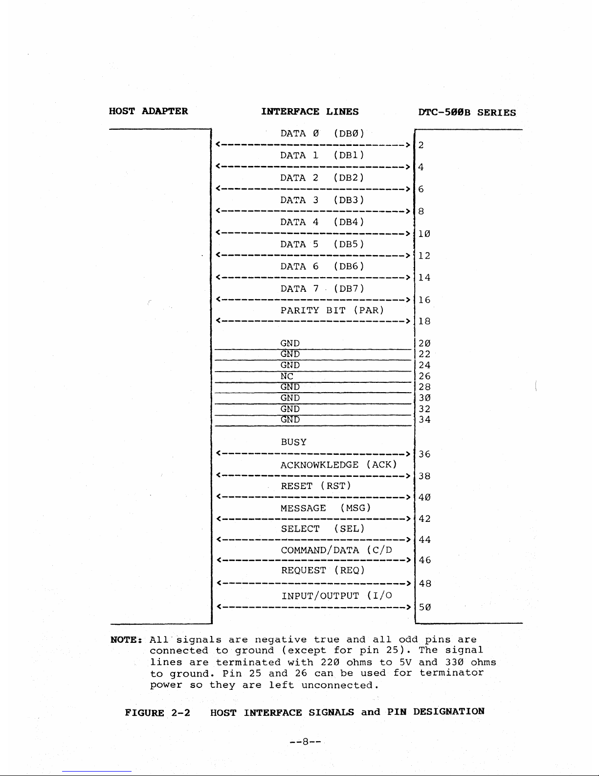
HOST
ADAPTER
INTERFACE
LINES
DTC-SeeB
SERIES
DATA
0 (DB0)
<---------------------------->
2
DATA
l
(DB1)
<---------------------------->
4
DATA
2 (DB2)
<---------------------------->
6
DATA
3
(DB3)
<---------------------------->
8
DATA
4
(DB4)
<---------------------------->
10
DATA
5
(DB5)
<---------------------------->
12
DATA
6
(DB6)
<---------------------------->
14
DATA
7 (DB7)
<---------------------------->
16
PARITY
BIT
(PAR)
<---------------------------->
18
GND
20
GND
22
GND
24
NC
26
GND
28
GND
30
__________
~GN~D~----------------t32
GND
34
BUSY
<---------------------------->
36
ACKNOWKLEDGE
(ACK)
<---------------------------->
38
RESET
(RST)
<---------------------------->
40
MESSAGE
(MSG)
<---------------------------->
42
SELECT
(SEL)
<---------------------------->
44
COMMAND/DATA
(C/D
<---------------------------->
46
REQUEST
(REQ)
<---------------------------->
48
INPUT/OUTPUT
(I/O
<---------------------------->
50
NOTE:
All
signals
are
negative
true
and
all
odd
pins
are
connected
to
ground
(except
for
pin
25).
The
signal
lines
are
terminated
with
220
ohms
to
5V
and
330
ohms
to
ground.
Pin
25
and
26
can
be
used
for
terminator
power
so
they
are
left
unconnected.
FIGURE
2-2
HOST
INTERFACE
SIGNALS
and
PIN DESIGNATION
--8--
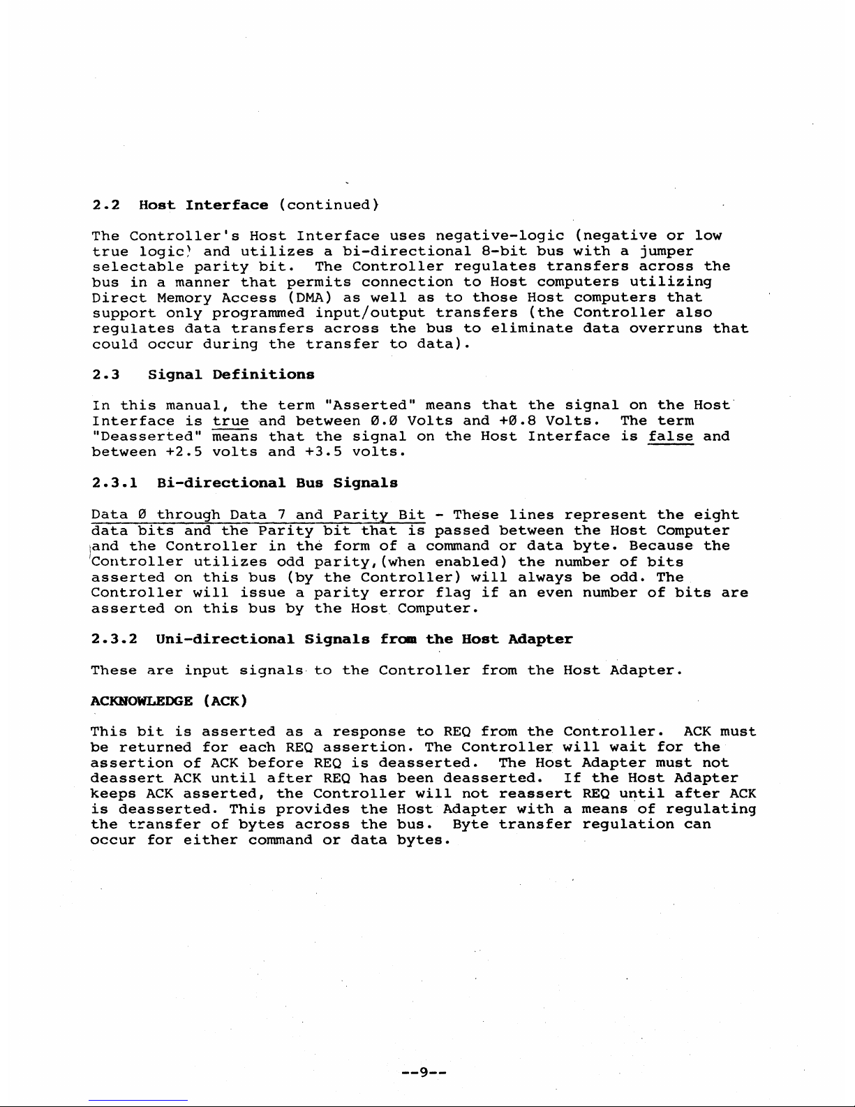
2.2
Host
Interface
(continued}
The
Controller's
Host
Interface
uses
negative-logic
(negative
or
low
true
logic~
and
utilizes
a
bi-directional
8-bit
bus
with
a
jumper
selectable
parity
bit.
The
Controller
regulates
transfers
across
the
bus
in a manner
that
permits
connection
to
Host
computers
utilizing
Direct
Memory
Access
(DMA)
as
well
as
to
those
Host
computers
that
support
only
programmed
input/output
transfers
(the
Controller
also
regulates
data
transfers
across
the
bus
to
eliminate
data
overruns
that
could
occur
during
the
transfer
to
data).
2.3
Signal
Definitions
In
this
manual,
the
term
"Asserted"
means
that
the
signal
on
the
Host
Interface
is
true
and
between
0.0
Volts
and
+0.8
Volts.
The
term
"Deasserted"
means
that
the
signal
on
the
Host
Interface
is
false
and
between
+2.5
volts
and
+3.5
volts.
-----
2.3.1
Bi-directional
Bus
Signals
Data
0
through
Data
7
and
Parity
Bit
-
These
lines
represent
the
eight
data
bits
and
the
Parity
bit
that
is
passed
between
the
Host
Computer
land
the
Controller
in
the
form
of
a
command
or
data
byte.
Because
the
'Controller
utilizes
odd
parity,
(when
enabled)
the
number
of
bits
asserted
on
this
bus
(by
the
Controller)
will
always
be
odd.
The
Controller
will
issue
a
parity
error
flag
if
an
even
number
of
bits
are
asserted
on
this
bus
by
the
Host
Computer.
2.3.2
Un
i-directional
Signals
from
the
Host
Adapter
These
are
input
signals
to
the
Controller
from
the
Host
Adapter.
ACKNOWLEDGE
(ACK)
This
bit
is
asserted
as
a
response
to
REO
from
the
Controller.
ACK
must
be
returned
for
each
REO
assertion.
The
Controller
will
wait
for
the
assertion
of
ACK
before
REO
is
deasserted.
The
Host
Adapter
must
not
deassert
ACK
until
after
REO
has
been
deasserted.
If
the
Host
Adapter
keeps
ACK
asserted,
the
Controller
will
not
reassert
REO
until
after
ACK
is
deasserted.
This
provides
the
Host
Adapter
with
a
means
of
regulating
the
transfer
of
bytes
across
the
bus.
Byte
transfer
regulation
can
occur
for
either
command
or
data
bytes.
--9--
2.3.2
Uni-directional
Signals
from
the
Host
Adapter
(continued)
RESET
(RST)
When
asserted,
this
bit
will
force
the
Controller
to
the
beginning
of
its
microcode
program
and
set
all
drive
parameters
to
their
default
value.
Reset
immediately
terminates
any
pending
command
without
the
transmission
of
the
status
or
message
bytes.
Any
error
status
request
(after
RST
has
been
asserted)
will
result
in
invalid
status
information
being
transferred.
All
Disk
Drive
interface
lines
are
deasserted.
Reset
must
be
asserted
for
a
minimum
of
250
nanoseconds
and
a maximum
of
10
seconds.
The
Controller
monitors
its
Host
Interface
and
waits
for
an
asserted
Select
(SEL)
signal
and
the
asserted
ID
bit
corresponding
to
the
Controller
after
Reset.
SELECT
(SEL)
When
asserted,
indicates
~he
beginning
of
the
command
transaction.
The
Host
Adapter
asserts
SEL
to
gain
the
attention
of
the
Controller.
A
Data
bit
on
the
bus
must
also
be
asserted
during
SEL
time
to
select
a .
Controller.
The
Controller
will
return
BUSY
as
acknowledgement
for
SEL.
After
the
assertion
of
BUSY,
the
Host
Adapter
will
deassert
SEL
and
the
data
bit
(ID
bit).
The
Controller
will
wait
until
SEL
is
deasserted
before
it
asserts
REQ. SEL
can
be
asserted
immediately
following
a
Reset.
--10--
2.3.3
Uni-directional
Signals
from
the
Controller
These
are
the
output
signals
from
the
Controller
to
the
Host
Adapter:
Input/Output
(I/O)
- When
asserted,
the
information
on
the
bi-
d~rectional
Bus
~s
driven
by
the
Controller.
When
deasserted,
the
information
on
the
bi-directional
Bus
is
driven
by
the
Host.
The
Host
may
use
this
signal
to
enable
its
Data
Bus
line
drivers.
Command/Data
(C/D)
- When
asserted,
the
information
bytes
transmitted
across
the
b~-d~rectional
Bus
are
command,
status,
or
message
bytes.
Ilhen
deasserted,
the
bytes
transmitted
across
the
bi-directional
Bus
are
data
bytes.
Busy
(BUSY) -
This
bit
is
asserted
in
response
to
the
Select
signal
and
ID
b~t
be~ng
asserted
from
the
Host
to
indicate
that
the
Controller's
Host
Interface
is
currently
in
use.
Busy
remains
asserted
through
the
message
phase.
Hessage
(MSG)
- When
asserted,
this
line
indicates
that
the
command
is
completed.
This
bit
is
always
followed
with
the
assertion
of
the
Tnput/Output
and
Request
signals.
Request
(REQ) -
This
bit
operates
in
conjunction
with
the
Input/Output,
Command/Data,
and
Message
signals.
See
Table
2-1
for
an
interpretation
of
these
signal
lines.
TABLE
2-1
Interpretation
of
Request
State
of
Signal
Lines
REQ
I/O
CD
MSG
Meaning
I
a d a d
Get
Command
byte
from
Host
Adapter
I
a
cl.
d d
Get
Data
byte
from
Host
Adapter
I
a a
d d
Send
Data
byte
to
Host
Adapter
I
a
a a d
Send
Status
byte
to
Host
Adapter
I
a a a a
Send
Message
byte
to
Host
Adapter
I
a =
asserted
d =
deasserted
2.3.4
Controller/Disk
Drive
Interface
Signals
Figures
2-3,
2-4,
2-5,
2-6,
2-7
and
2-8
show
the
name,
pin
designation,
and
direction
of
the
signals
on
the
Controller's
drive
interface.
These
interface
signals
are
explained
in
the
corresponding
Disk
Drive
documentation.
--11--
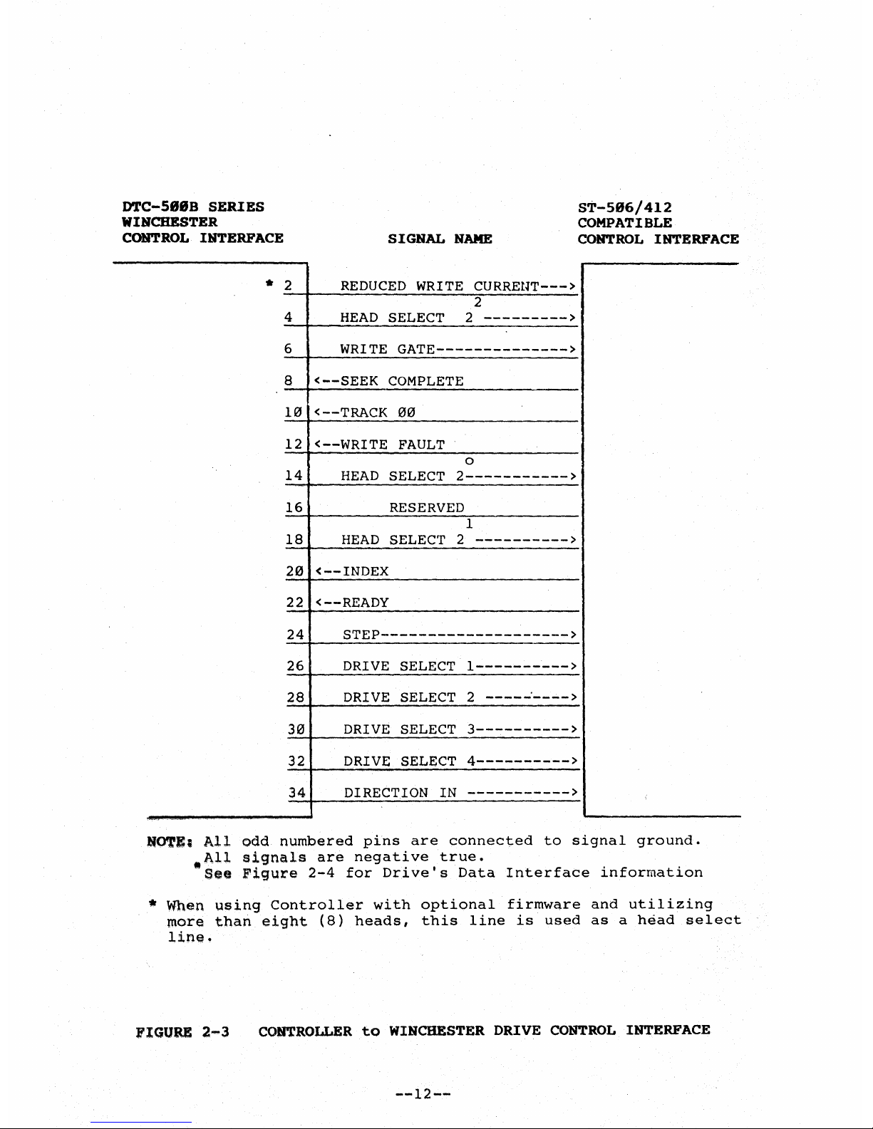
D'l'C-588B
SERIES
WINCHESTER
CONTROL
INTERFACE
*
2
4
6
8
113
12
14
16
18
213
22
24
26
28
313
32
34
SIGNAL
NAME
REDUCED
WRITE
CURREUT--->
2
HEAD
SELECT 2
--------->
WRITE
GATE-------------->
<--SEEK
COMPLETE
<--TRACK
1313
<--WRITE
FAULT
0
HEAD
SELECT
2----------->
RESERVED
1
HEAD
SELECT 2
---------->
<--INDEX
<--READY
STEP-------------------->
DRIVE SELECT
1---------->
DRIVE SELECT 2
-----'---->
DRIVE SELECT
3---------->
DRIVE
SELECT
4---------->
DIRECTION IN
----------->
ST-586/412
COMPATIBLE
CONTROL
INTERFACE
NOTE;
All
odd
numbered
pins
are
connected
to
signal
ground
.
• AII
signals
are
negative
true.
See
Figure
2-4
for
Drive's
Data
Interface
information
* When
using
Controller
with
optional
firmware
and
utilizing
more
than
eight
(8)
heads,
this
line
is
used
as a head
select
lina.
li'IGUM
2-3
CONTROLLER
to
WINCHESTER DRIVE
CONTROL
INTERFACE
--12--
DTC-51iJ1iJB
SERIES
WINCHESTER
DATA
INTERFACE
___
L
__
---
-
1
2
3
4
5
6
7
8
9
HI
11
12
13
14
15
16
17
18
19
_20
SIGI!IAL
NAMES
<---DRIVE
SELECTED
RESERVED
RESERVED
RESERVED
RESERVED
RESERVED
+MFM
WRITE
DATA-------->
-MFM
WRITE
DATA-------->
<---+MFM
READ
DATA
<----MFM
READ
DATA
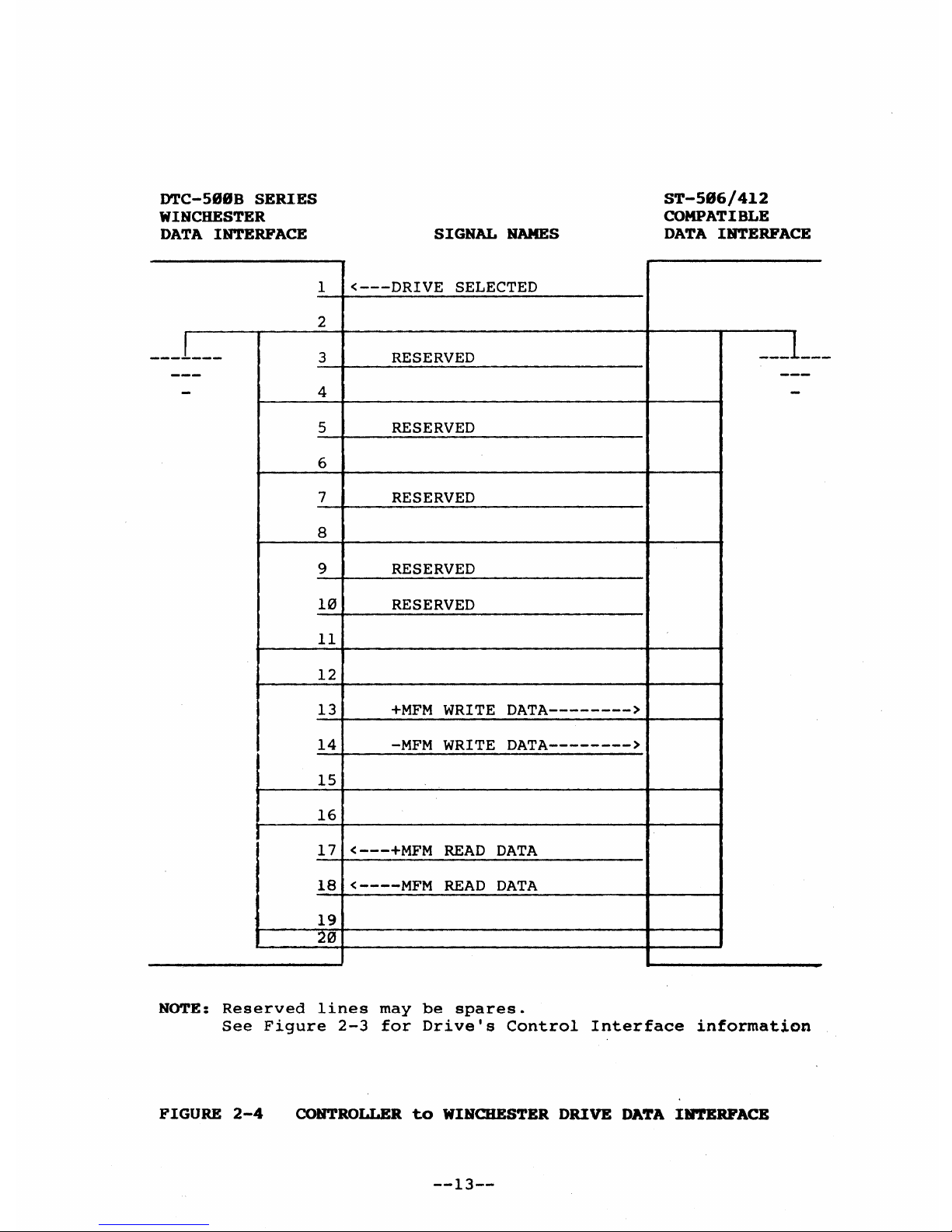
NOTE:
Reserved
lines
may
be
spares.
ST-51iJ6/412
COMPATIBLE
DATA
INTERFACE
__
L _
---
-
See
Figure
2-3
for
Drive's
Control
Interface
information
FIGURE
2-4
COII1TROLLER
to
WINCBES'rER
DRIVE
DATA
1II1TERPACE
--13--
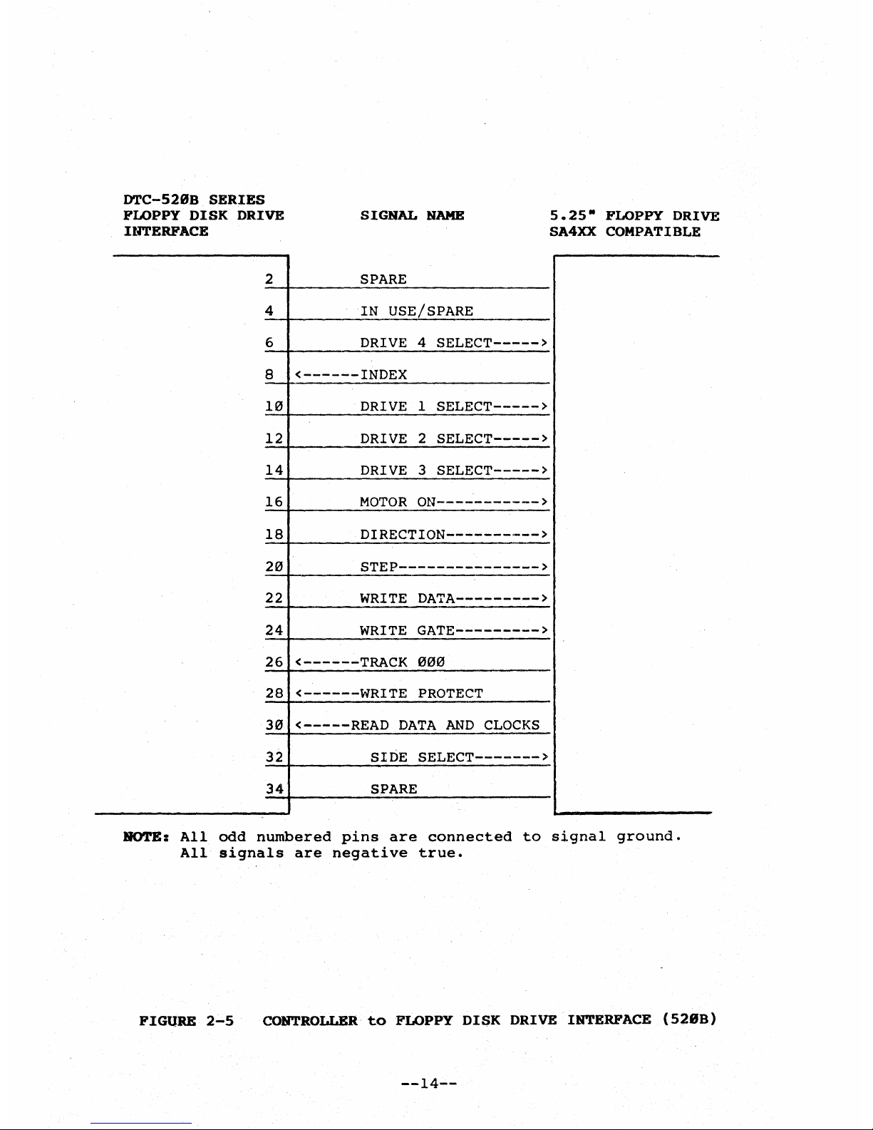
DTC-52i1B
SERIES
FLOPPY
DISK
DRIVE
IlITERFACE
2
4
6
8
10
12
14
16
18
20
22
24
26
28
30
32
34
SIGNAL
NAME
SPARE
IN
USE/SPARE
DRIVE 4
SELECT----->
<------INDEX
DRIVE 1
SELECT----->
DRIVE 2
SELECT----->
DRIVE 3
SELECT----->
MOTOR
ON----------->
DIRECTION---------->
STEP--------------->
WRITE
DATA--------->
WRITE
GATE--------->
<------TRACK
000
<------WRITE
PROTECT
<-----READ
DATA
AND
CLOCKS
SIDE
SELECT------->
SPARE
5 •
25·
FLOPPY DRIVE
SA4XX COMPATIBLE
NOTE:
All
odd
numbered
pins
are
connected
to
signal
ground.
All
signals
are
negative
true.
FIGURE
2-5
CONTROLLER
to
FLOPPY
DISK
DRIVE INTERFACE
(528B)
--14--

535B
CONTROLLER
SA8XX
INTERFACE
EXTERNAL
\~RITE
CURRENT
SWITCHING---->
2
<----TRUE
READY
*
8
<----TWO
SIDED
*
+
10
<----DISK
CHANGE
*
12
SIDE
SELECT
*
+
---------------->
14
IN
USE * ----------------------->
16
110TOR
ON * (HEAD
LOAD)---------->
18
<----INDEX
20
<----READY
22
<----SECTOR
24
DRIVE SELECT 1
(SIDE
SELECT
OPT)+
--->
26
DRIVE SELECT
2
(SIDE
SELECT
OPT)+
--->
28
DRIVE SELECT 3
(SIDE
SELECT
OPT)+
--->
30
DRIVE
SELECT 4
(SIDE
SELECT
OPT)+
--->
32
DIRECTION SELECT
(SIDE
SELECT
OPT)+-->
34
STEP---------------------------->
36
WRl'rE
DATA
--------------------->
38
WRITE
GATE---------------------->
40
<----TRACK
00
42
<----WRITE
PROJECT
44
<----READ
DATA
46
<----SEP
DATA
48
<----SEP
CLOCK
50
NOTE:
All
odd
numbered
pins
are
connected
to
signal
ground.
All
signals
are
negative
true.
*
Jumper
enabled
alternate
I/O
lines.
+
SA860
only.
FIGURE
2-6
CONTROLLER
to
FLOPPPY
DISK
DRIVE
INTERFACE(535B)
--15--
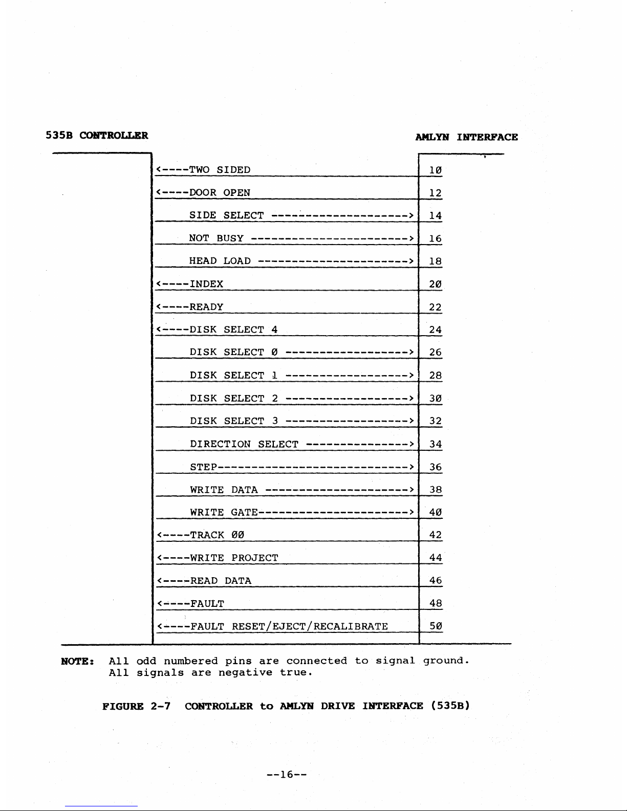
535B
CONTROLLER
AMLYH
INTERFACE
<----TWO
SIDED
1~
<----DOOR
OPEN
12
SIDE
SELECT
-------------------->
14
NOT
BUSY
----------------------->
16
HEAD
LOAD
---------------------->
18
<----INDEX
20
<----READY
22
<----DISK
SELECT 4
24
DISK SELECT 0
------------------>
26
DISK SELECT 1
------------------>
28
DISK SELECT 2
------------------>
30
DISK SELECT 3
------------------>
32
DIRECTION SELECT
--------------->
34
STEP---------------------------->
36
WRITE
DATA
--------------------->
38
WRITE
GATE---------------------->
40
<----TRACK
00
42
<----WRITE
PROJECT
44
<----READ
DATA
46
<----FAULT
48
<----FAULT
RESET/EJECT/RECALIBRATE
50
NOTE:
All
odd
numbered
pins
are
connected
to
signal
ground.
All
signals
are
negative
true.
FIGURE
2-7
CONTROLLER
to
AMLYH
DRIVE
INTERFACE
(535B)
--16--
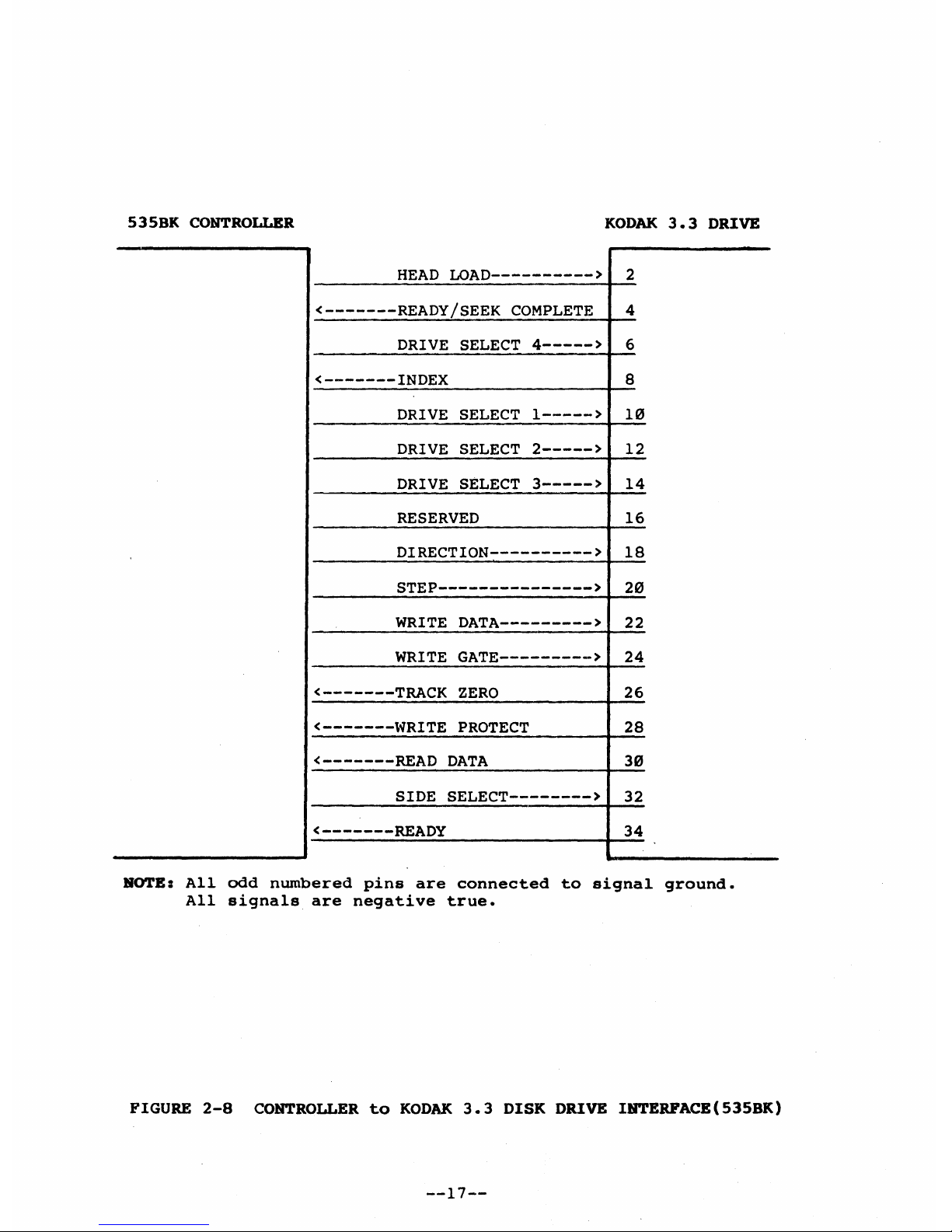
535BK
CONTROLLER
KODAK
3.3
DRIVE
HEAD
LOAD---------->
2
<-------READy/SEEK
COMPLETE
4
DRIVE
SELECT
4----->
6
<-------INDEX
8
DRIVE SELECT
1----->
1'"
DRIVE
SELECT
2----->
12
DRIVE
SELECT
3----->
14
RESERVED
16
DIRECTION---------->
18
STEP--------------->
2'"
WRITE
DATA--------->
22
WRITE
GATE--------->
24
<-------TRACK
ZERO
26
<
-------\~RITE
PROTECT
28
<-------READ
DATA
3'"
SIDE
SELECT-------->
32
<-------READy
34
NOTE:
All
odd
numbered
pins
are
connected
to
signal
ground.
All
signals
are
negative
true.
FIGURE
2-8
CONTROLLER
to
KODAK
3.3
DISK
DRIVE INTERFACE{535BK)
--17--
2.4
Sequence
of
Operation
The
Controller
performs
an
internal
RAM
test
upon
power-up.
If
there
is
a
RAM
failure,
the
Controller
will
display
an
error
code
18
(hex)
and
will
not
respond
to
the
Host.
Commands
are
issued
to
the
DTC-500B
Series
Controller
via
the
Host
Adapter
following
a
defined
protocol
(SASI).
The
Host
initiates
a
command
sequence
by
selecting
the
Controller
on
the
bus.
If
the
Controller
is
not
busy,
it
requests
command
bytes
from
the
Host
for
task
execution.
(Command
structure
is
described
in
Section
3.0).
Upon
reception
of
the
last
command
byte,
the
Controller
begins
execution
of
the
command.
For
the
data
transfer
commands,
a
check
is
performed
on
the
disk
address
and
status
is
flagged
if
it
exceeds
the
drive
limits.
The
data
is
stored
in
a
sector
buffer
before
any
transfer
to
the
Host
or
disk
drive
takes
place.
This
buffer
eliminates
any
possibility
of
data
overruns
between
the
Host
and
the
disk.
Upon
completion
of
the
command,
the
Controller
will
send
the
completion
status
and
the
message
byte
to
the
Host.
If
an
error
is
indicated,
further
delineation
of
the
completion
status
r:Iay
be
requested
by
the
Host
issuing
the
appropriate
sense
commands.
Request
Sense
Command
will
clear
the
error
in
the
LED's.
Parity
must
be
enabled
or
disabled
on
both
the
Host
and
Controller.
If
parity
is
enabled,
the
Controller
will
generate
ODD
parity
for
all
data
it
puts
on
the
Host
Bus
and
it
will
check
for
ODD
parity
for
all
data
it
receives
from
the
Host
Bus.
If
parity
is
disabled,
the
Controller
does
not
generate
or
check
parity.
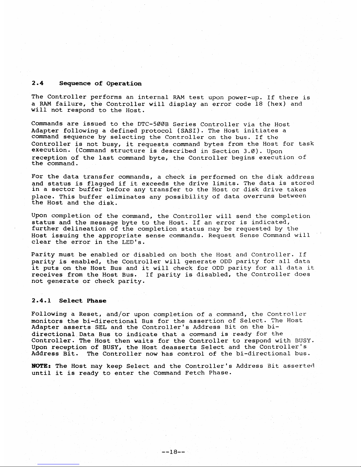
2.4.1
Select
Phase
Following
a
Reset,
and/or
upon
completion
of
a
command,
the
Controller
monitors
the
bi-directional
Bus
for
the
assertion
of
Select.
The
Host
Adapter
asserts
SEL
and
the
Controller's
Address
Bit
on
the
bi-
directional
Data
Bus
to
indicate
that
a
command
is
ready
for
the
Controller.
The
Host
then
waits
for
the
Controller
to
respond
with
BUSY.
Upon
reception
of
BUSY,
the
Host
deasserts
Select
and
the
Controller's
Address
Bit.
The
Controller
now
has
control
of
the
bi-directional
bus.
HOTE:
The
Host
may
keep
Select
and
the
Controller's
Address
Bit
asserteo
until
it
is
ready
to
enter
the
Command
Fetch
Phase.
--18--
2.4.2
Command
Phase
After
the
Host
deasserts
Select
and
the
Controller's
Address
Bit,
the
Controller
asserts
the
Command/Data
(C/D)
bit
to
indicate
a Command
transfer,
and
deasserts
r/o
to
indicate
an
output
from
the
Host.
The
command
bytes
are
transferred
OVer
the
bi-directional
bus
one
byte
with
each
REO/ACK
handshake
protocol,
until
all
command
bytes
are
transferred
to
the
Controller.
The
Command
Phase
ends
after
the
last
REO
pulse
from
the
Controller
is
deasserted.
NOTE:
The
Host
must
not
assert
ACK
until
after
REO
is
asserted
and
must
not
deassert
ACK
until
after
REO
is
deasserted.
The
Controller
waits
until
ACK
from
the
previous
byte
transfer
is
deasserted
before
it
reasserts
REO
to
transfer
the
next
byte.
This
provides
a
means
for
the
Host
to
regulate
the
byte
transfer
across
the
bi-directional
bus.
2.4.3
Data
Phase
This
phase
is
skipped
when
the
command
does
not
require
a
transfer
of
data.
If
a
Read
or
Write
data
transfer
is
required
for
the
command,
the
following
occurs:
a.
The
Controller
deasserts
the
Command/Data
(C/o)
line
to
indicate
a
Data
transfer.
b.
Depending
on
the
command
type
(read
or
write)
the
I/O
line
(for
the
bi-directional
bus)
is
asserted
or
deasserted
by
the
Controller.
c.
The
data
is
transferred
(one
byte
at
a
time)
with
the
same
REO/ACK
handshake
protocol
used
in
the
Command
Phase.
d.
After
all
data
bytes
are
transferred,
the
Controller
exits
this
phase
and
enters
the
Status
phase.
2.4.4
Status
and
Message
Phase
After
all
the
Command
and
Data
bytes
have
been
transferred,
a
Status
byte
is
placed
on
the
bi-directional
bus
by
the
Controller.
(REO,C/D,
and
I/O
are
asserted,
MSG
is
deasserted).
The
Controller
waits
for
ACK
from
the
!lost.
Upon
receipt
of
ACK,
the
status
byte
is
transferred.
The
Controller
asserts
REO,
C/O,
I/O
and
MSG
to
indicate
to
the
Host
that
the
command
is
complete.
This
action
can
be
used
to
generate
an
interrupt
in
the
Host.
After
the
Host
responds
with
ACK,
the
Controller
will
deassert
BUSY, REO,
C/O,
I/O,
and
MSG.
This
completes
the
normal
command
sequence
and
the
Controller
is
ready
to
be
Selected
by
the
Host
Adapter
for
the
next
command
sequence.
--19--
SEL
D~
BSY
NOTES:
TIMING
DIAGRAMS
Timing
Requirementa
for
Controller
Selection
,-----------------
,
,
1<---
>~I----------~
I lOOnal
1 1
1
1
, ,-------r----------------------
1<------->1<------->
I 4 ms 1
no
time
1
max
1
limit
1.
SEL
must
be
deasserted
before
the
Controller
will
assert
RBQ.
·2.
After
Power
On
or
Reset,
when
the
first
command
is
issued,
it
may
take
the
Controller
a maximum
of
4 ms
to
respond
with
BUSY.
The
BUSY
response
time
for
all
successive
commands
will
be
within
50
us.
FIGURE
2-9
TIMING
DIAGRAMS
(sheet
I
of
6)
--20--
TIMING
DIAGRAMS
Timing
Requir~nts
for
Command
Transfer
Phase
(from
Host
Adapter.
one
byte)
1/0
____
x
1
___
I
CID f'--------------------------------------
___
1,-------------------------------------
MSG
X
REO
ACK
DB
NOTES:
1
1
1<
->1
_______________________________
_
I
588nsl
I
min
I
I 1
1
I 1 1 1
1<----->1<------>1<------>1
Ino
time I 588
ns
lno
time
I
I
limit
1
typ
I
limit
I
I I I
Data
driven
by
_______________________
~-----.X-----X
Host
Adapter
I
I---r-I'"'-----'
1
<--->
1 1
<->
I
1188nsl
18nsl
1
max
1
1.
I/O*,
C/D*,
MSG*
changes
500
ns
min
before
the
1st
REO
for
the
phase
and
remain
unchanged
until
the
Controller
goes
into
the
next
phase.
2.
Data
driven
by
the
Controller
is
stable
100ns
min
at
the
Host
Adapter
end
before
REO*
is
asserted
and
0ns
min
after
REO*
is
deasserted.
3.
Data
driven
by
the
Host
Adapter
is
stable
100ns
max
(at
the
Host
Adapter
end)
after
ACK*
is
asserted
and
0ns
min
after
REO*
is
deasserted.
FIGURE
2-9
TIMING
DIAGRAMS
(sheet
2
of
6)
--21--
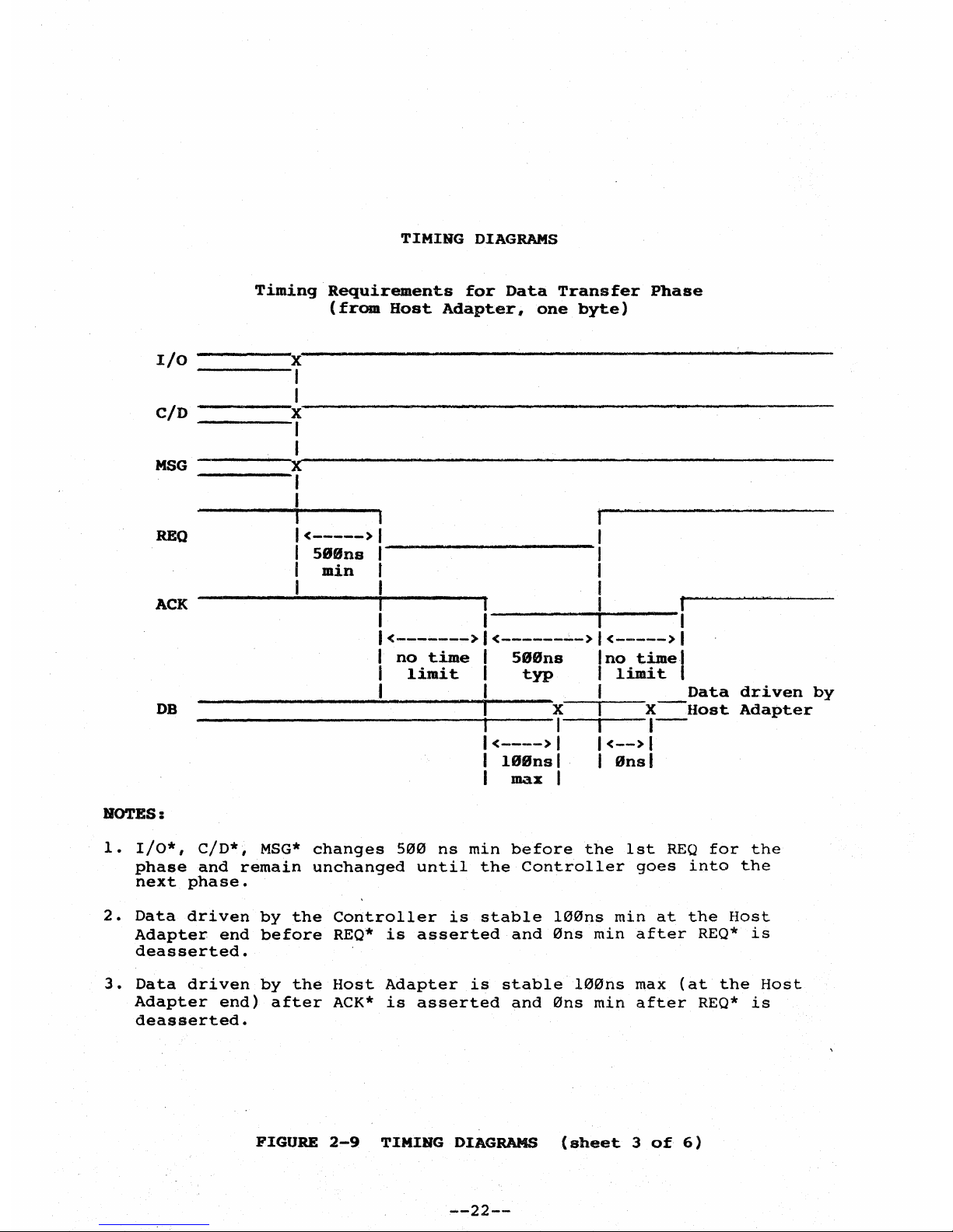
I/O
C/D
MSG
REO
ACK
DB
1!if00ES:
TIMING
DIAGRAMS
Timing
Requirements
for
Data
Transfer
Phase
(from
Host
Adapter,
one
byte)
X
I
I
X
I
I
x:
I
I
I
1<----->
I
51Ulns
I
min
I
I
---------------,
I
f
I
I
I
I I
<------->1<-------->1<----->1
no
time
I 5BI'lns I
no
time
I
limit
I
typ
I
limit
I I
Data
driven
by
------------------~--------~l~----~x
I
X---Host
Adapter
-----------+1--1
I
I-
I
<---->
I I
<-->
I
I
II'lBnsl
I
I'lnsl
I
max
I
1.
1/0*,
C/D*,
MSG*
changes
SI'lI'l
ns
min
before
the
1st
REO
for
the
phase
and
remain
unchanged
until
the
Controller
goes
into
the
next
phase.
2.
Data
driven
by
the
Controller
is
stable
ll'll'lns
min
at
the
Host
Adapter
end
before
REO*
is
asserted
and
I'Ins
min
after
REO*
is
deasserted.
3.
Data
driven
by
the
Host
Adapter
is
stable
11'11'1ns
max
(at
the
Host
Adapter
end)
after
ACK*
is
asserted
and
I'Ins
min
after
REO*
is
deasserted.
FIGURE
2-9
TIMING
DIAGRAMS
(sheet
3
of
6)
--22--
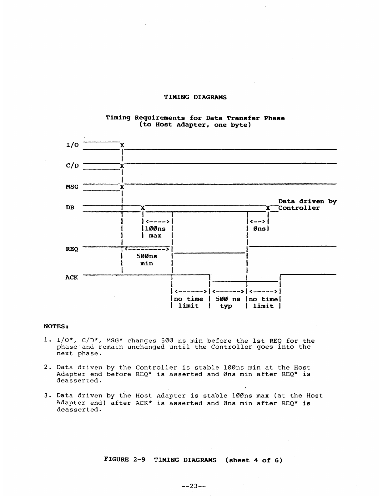
I/O
C/D
MSG
DB
REO
ACK
NOTES:
TIMING
DIAGRAMS
Timing
Requirements
for
Data
Transfer
Phase
(to
Host
Adapter,
one
byte)
_________ x ________________________________________________ _
I
------_1---------------------------------------
______
...:X
I
------_1------------------------------------------
_____
x
I
I
Data
driven
by
_
________
~I~---x.
_____
-r
________________
~~--x--Controller
I
1-
I
1--
I
1<---->
<-->1
I
1100ns
0nsl
I I
max
I
1<--
-->
I
500ns
I
I
min
___
+-
__
1
I
<------>1<------>
<----->1
no
time
580
ns
Ino
time
I
limit
typ
I
limit
I
1.
1/0*,
C/D*,
HSG*
changes
500
ns
min
before
the
1st
REO
for
the
phase
and
remain
unchanged
until
the
Controller
goes
into
the
next
phase.
2.
Data
driven
by
the
Controller
is
stable
100ns
min
at
the
Host
Adapter
end
before
REQ*
is
asserted
and
0ns
min
after
REQ*
is
deasserted.
3.
Data
driven
by
the
Host
Adapter
is
stable
100ns
max
(at
the
Host
Adapter
end)
after
ACK*
is
asserted
and
0ns
min
after
REQ*
is
deasserted.
FIGURE
2-9
TIMING
DIAGRAMS
(sheet
4
of
6)
--23--
 Loading...