

Page 1
User Manual
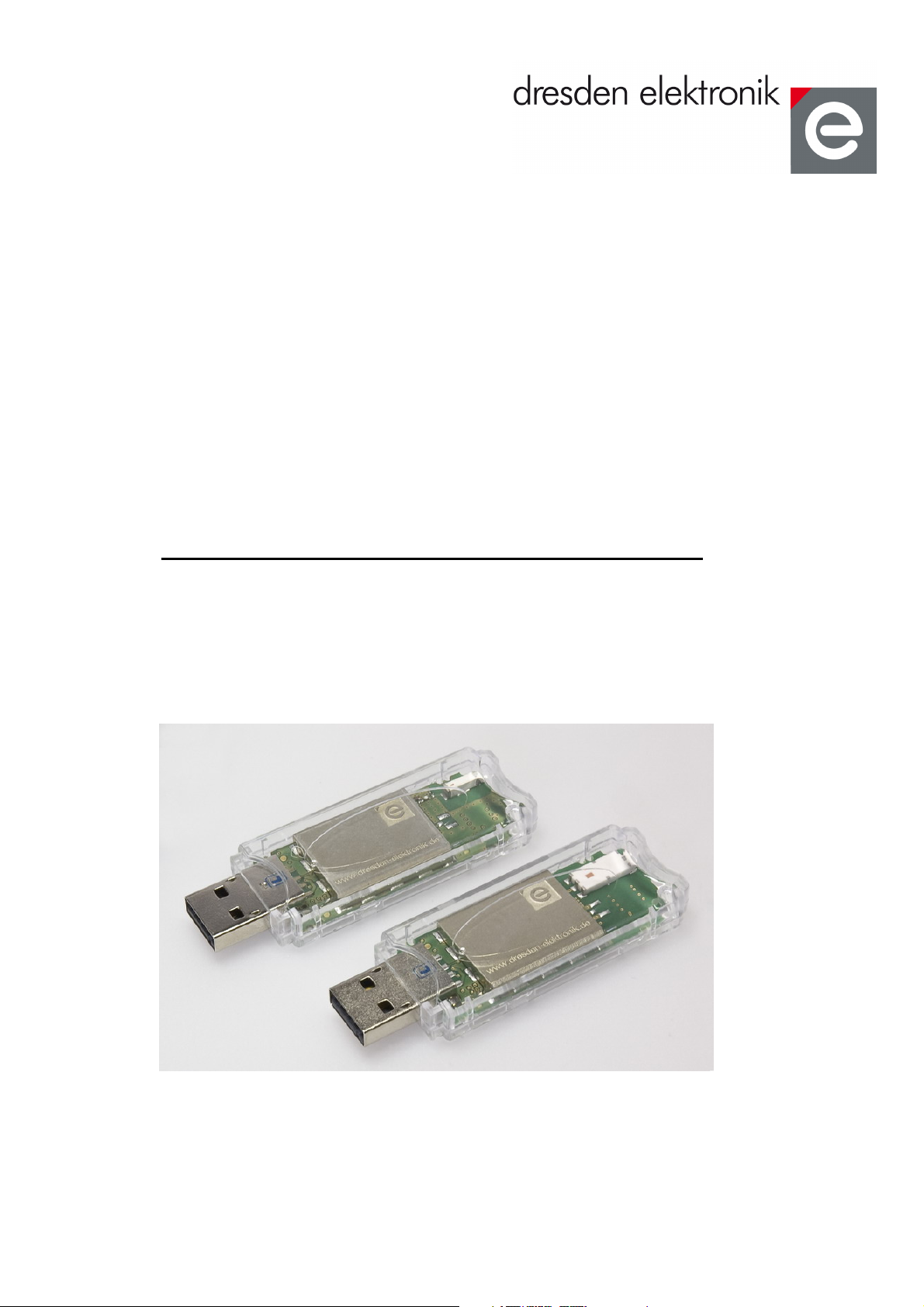
USB Radio Sticks
deRFusb-23E00
deRFusb-23E06
deRFusb-13E00
deRFusb-13E06
Document Version V01.00
2011-04-15
Page 2

User Manual
Version 01.00
2011-03-31
USB radio sticks deRFusb
Table of contents
1. Overview ......................................................................................................................... 5
2. Application ....................................................................................................................... 5
3. Features .......................................................................................................................... 5
4. Technical data ................................................................................................................. 7
5. Mechanical size ............................................................................................................... 9
6. Pin assignment .............................................................................................................. 10
7. Programming ................................................................................................................. 14
7.1. JTAG interface ..................................................................................................... 14
7.2. USB interface ....................................................................................................... 14
7.3. Required hardware ............................................................................................... 14
7.4. Programming and debugging details .................................................................... 15
8. Onboard transceiver ...................................................................................................... 16
9. Onboard flash (option) ................................................................................................... 17
10. Radio certification .......................................................................................................... 18
10.1. United States (FCC) ............................................................................................. 18
10.2. European Union (ETSI) ........................................................................................ 19
11. Ordering information ...................................................................................................... 20
12. Revision notes ............................................................................................................... 21
dresden elektronik
ingenieurtechnik gmbh
Enno-Heidebroek-Str. 12
01237 Dresden / Germany
Tel.: 0351 – 31 85 00
Fax: 0351 – 3 18 50 10
wireless@dresden-elektronik.de
www.dresden-elektronik.de
Page 2 of 22
Page 3
User Manual
Version 01.00
2011-03-31
USB radio sticks deRFusb
Document history
Date Version Description
2011-03-31 01.00 Initial version
Mailing list
Firm Division / Name
DE APA
Author / Check / Release
Firm Division / Name
Author DE Dev. / APA
Check
release
dresden elektronik
ingenieurtechnik gmbh
Enno-Heidebroek-Str. 12
01237 Dresden / Germany
Tel.: 0351 – 31 85 00
Fax: 0351 – 3 18 50 10
wireless@dresden-elektronik.de
www.dresden-elektronik.de
Page 3 of 22
Page 4
User Manual
A
A
D
A
E
F
G
I
J
M
M
P
R
S
T
U
U
U
W
Version 01.00
2011-03-31
USB radio sticks deRFusb
Abbreviations
Abbreviation Description
ADC
AES
CE
DAC
ETSI
FCC
GPIO
nalog to Digital Converter
dvanced Encryption Standard
(Applications) - Consumer Electronics
igital to
nalog Converter
uropean Telecommunications Standards Institute
ederal Communications Commission
enerals Purpose Input Output
IC (Certification) - Industry Canada
ISM
JTAG
MAC
MCU, µC
PWM
RF
SPI
TWI
ndustrial, Scientific and Medical frequency band
oint Test Action Group
edium Access Control
icrocontroller Unit
ulse Width Modulation
adio Frequency
erial Peripheral Interface
wo-Wire Serial Interface
UART
USART
USB
WPAN
dresden elektronik
ingenieurtechnik gmbh
Enno-Heidebroek-Str. 12
01237 Dresden / Germany
niversal Asynchronous Receiver Transmitter
niversal Synchronous/Asynchronous Receiver Transmitter
niversal Serial Bus
ireless Personal Area Network
Tel.: 0351 – 31 85 00
Fax: 0351 – 3 18 50 10
wireless@dresden-elektronik.de
www.dresden-elektronik.de
Page 4 of 22
Page 5

User Manual
Version 01.00
2011-03-31
USB radio sticks deRFusb
1. Overview
The compact designed USB radio sticks deRFusb-23E00 and deRFusb-13E00 contain a
powerful CORTEX-M3 microcontroller with 256 kBytes High-Speed Flash. Additional flash
memory to store user defined data is provided using the USB radio sticks deRFusb-23E06
and deRFusb-13E06, it is usable as mass storage device.
Depending on the transmission frequency of 2.4 GHz - deRFusb-23E00/06 - or 868/915 MHz
- deRFusb-13E00/06 - the ATMEL low-power transceivers AT86RF231 or alternatively
AT86RF212 are integrated. They provide a complete radio transceiver interface between the
antenna and the microcontroller and an extended functional range such as a 128-Bit AES
hardware engine to assure data security.
The USB radio sticks provide a programming and debugging interface to the user, by default
via USB.
2. Application
The main applications for the USB radio sticks deRFusb-23E00/06 and deRFusb-13E00/06
are:
• 2.4GHz and Sub-GHz range IEEE 802.15.4
• ZigBee® Pro
• ZigBee® RF4CE
• ZigBee® IP
• 6LoWPAN
• SP100
• Wireless Sensor Networks (WSN)
• industrial and home controlling and monitoring
3. Features
The USB radio sticks deRFusb-23E00 and deRFusb-23E06 offer the following features:
• compact size (in case): 71.0 x 23.0 x 8.7 mm
• USB powered
• 3 free programmable status LEDs
• RF shielding
• Debugging/Programming interfaces: 1 x DBGU (Debug-Unit) or 1 x JTAG with 10 pin
connector mounting option, USB
• Onboard transceiver and chip ceramic antenna 2.4GHz
• Optional: onboard 2 GByte flash
• Certification: FCC, IC, conformity ETSI/CE
dresden elektronik
ingenieurtechnik gmbh
Enno-Heidebroek-Str. 12
01237 Dresden / Germany
Tel.: 0351 – 31 85 00
Fax: 0351 – 3 18 50 10
wireless@dresden-elektronik.de
www.dresden-elektronik.de
Page 5 of 22
Page 6
User Manual
Version 01.00
2011-03-31
USB radio sticks deRFusb
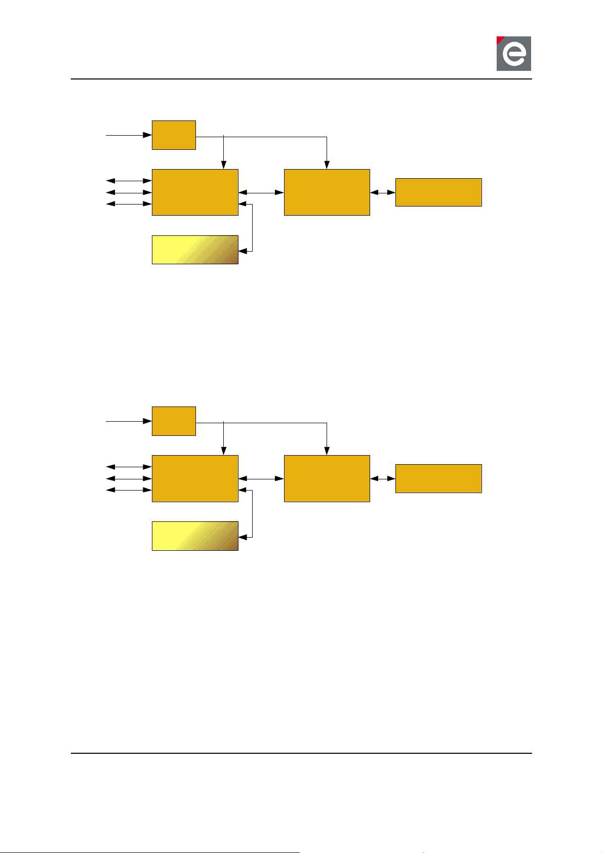
The block diagram below shows layout and interaction of the main deRFusb-23E00/06 components:
VUSB
4.5 .. 5.5V
JTAG
DBGU
USB
Option:
VCC
ATSAM3S4BA AT86RF231 Chip antenna
2 GByte Flash
VCC
3.3V
SPI
MMC
Figure 1: block diagram deRFusb-23E00 / 06
The deRFusb-13E00 and deRFusb-13E06 offer the same features like the deRFusb-23E00
/06 except the built-in Sub-GHz transceiver and onboard Sub-GHz chip antenna.
• Onboard transceiver and chip ceramic antenna for Sub-GHz
Layout and interaction of the main deRFusb-13E00/06 components:
VUSB
4.5 .. 5.5V
VCC
VCC
3.3V
JTAG
DBGU
USB
Option:
ATSAM3S4BA AT86RF212 Chip antenna
2 GByte Flash
SPI
MMC
Figure 2: block diagram deRFusb-13E00 / 06
dresden elektronik
ingenieurtechnik gmbh
Enno-Heidebroek-Str. 12
01237 Dresden / Germany
Tel.: 0351 – 31 85 00
Fax: 0351 – 3 18 50 10
wireless@dresden-elektronik.de
www.dresden-elektronik.de
Page 6 of 22
Page 7

User Manual
Version 01.00
2011-03-31
USB radio sticks deRFusb
4. Technical data
Table 1: Mechanical data
Mechanical
Radio module
Size (length x width x height) 71.0 x 23.0 x 8.7 mm (in case)
63.5 x 19.0 x 5.5 mm (without case)
Connectors
USB chassis plug type A
10 pin header - connection option 2 x 5 pins, 1.27 mm pitch
Table 2: Environment
Temperature and humidity range
Min Typ Max Unit
Working area T_work - 40 +85 °C
Working area 25 80 % r.H.
Table 3: Electrical data
Electrical (VUSB = 5.0VDC)
Parameter Min Typ Max Unit
Supply voltage VUSB 4.5 5.0 5.5 VDC
Current
consumption
I_TXon (TX_PWR = 3) 51 mA
I_TXoff 32 mA
I_sleep TBD mA
I_RXon TBD mA
dresden elektronik
ingenieurtechnik gmbh
Enno-Heidebroek-Str. 12
01237 Dresden / Germany
Tel.: 0351 – 31 85 00
Fax: 0351 – 3 18 50 10
wireless@dresden-elektronik.de
www.dresden-elektronik.de
Page 7 of 22
Page 8

User Manual
Version 01.00
2011-03-31
Table 4: Radio data transmission
USB radio sticks deRFusb
Radio (VUSB = 5.0VDC)
Parameter / feature Min Typ Max Unit
deRFusb-23E00/06
Antenna Chip ceramic
Antenna gain +1.3
- 0.5
Antenna diversity: no
Range line of sight >200
Frequency range 2.4
Transmitting
power conducted
TX_PWR = 0
+0.5
Receiver sensitivity - 101
Data rate 250
500
1
2
dBi (peak)
dBi (average)
m
GHz
dBm
dBm
kb/s
kb/s
Mb/s
Mb/s
deRFusb-13E00/06
Antenna Chip ceramic
Antenna gain - 0.7
- 2.6
Antenna diversity: no
Range line of sight >200
Frequency range 868
915
Transmitting
power conducted
TX_PWR = 0
+3.6
Receiver sensitivity - 110
Data rate 20
40
250
500
1
dBi (peak)
dBi (average)
m
MHz (band)
dBm
dBm
kb/s
kb/s
kb/s
kb/s
Mb/s
dresden elektronik
ingenieurtechnik gmbh
Enno-Heidebroek-Str. 12
01237 Dresden / Germany
Tel.: 0351 – 31 85 00
Fax: 0351 – 3 18 50 10
wireless@dresden-elektronik.de
www.dresden-elektronik.de
Page 8 of 22
Page 9

User Manual
63.5 mm
19.0 mm
Version 01.00
2011-03-31
USB radio sticks deRFusb
5. Mechanical size
height 5.5 mm
Figure 3: Size deRFusb-23E00 and deRFusb-23E06
Placed in case the mechanical size is 71.0 x 23.0 x 8.7 mm (length x width x height).
These dimensions are the same at the deRFusb-13E00 and deRFusb-13E06 radio sticks.
Figure 4: deRFusb-13E00 and deRFusb-13E06
The connector for all radio stick design versions is USB type A.
Figure 5: USB type A connection
dresden elektronik
ingenieurtechnik gmbh
Enno-Heidebroek-Str. 12
01237 Dresden / Germany
Tel.: 0351 – 31 85 00
Fax: 0351 – 3 18 50 10
wireless@dresden-elektronik.de
www.dresden-elektronik.de
Page 9 of 22
Page 10

User Manual
Version 01.00
2011-03-31
USB radio sticks deRFusb
6. Pin assignment
The 10 pin connector offers the programming interface (JTAG) and debugging interface (Debug RXD and Debug TXD) to the user. It is directly accessible from the USB stick bottom
side.
Figure 6: Top and bottom overlay deRFusb-23E06 and deRFusb-23E00 (without IC4)
X2 pins: 2 .... 10
1 ..... 9
1.27 mm pitch
Figure 7: 10 pin connector with footprint receptacle
dresden elektronik
ingenieurtechnik gmbh
Enno-Heidebroek-Str. 12
01237 Dresden / Germany
Tel.: 0351 – 31 85 00
Fax: 0351 – 3 18 50 10
wireless@dresden-elektronik.de
www.dresden-elektronik.de
Page 10 of 22
Page 11

User Manual
Version 01.00
2011-03-31
USB radio sticks deRFusb
Figure 8: Top overlay deRFusb-13E06 and deRFusb-13E00 (without IC4)
X2 pins: 2 .... 10
1 ..... 9
1.27 mm pitch
Figure 9: 10 pin connector with footprint receptacle
dresden elektronik
ingenieurtechnik gmbh
Enno-Heidebroek-Str. 12
01237 Dresden / Germany
Tel.: 0351 – 31 85 00
Fax: 0351 – 3 18 50 10
wireless@dresden-elektronik.de
www.dresden-elektronik.de
Page 11 of 22
Page 12

User Manual
Version 01.00
2011-03-31
Table 5: Pin assignment of deRFusb-23E00/06 and deRFusb-13E00/06
USB radio sticks deRFusb
µC Pin name function comments
USB connector
56 DDM USB DM
57 DDP USB DP
10 pin connector
53 PB7/TCK/SWCLK JTAG TCK pin 1
GND pin 2
49 PB5/TWCK1/PWML0/WKUP13/TDO JTAG TDO pin 3
VCC pin 4
51 PB6/TMS/SWDIO JTAG TMS pin 5
39 NRST /Reset pin 6
VCC pin 7
30 PA9/URXD0/NPCS1/PWMFI0 Debug RXD pin 8
33 PB4/TWD1/PWMH2/TDI JTAG TDI pin 9
29 PA10/UTXD0/NPCS2 Debug TXD pin 10
Miscellaneous
13 PA19/RK/PWML0/A15/AD2 LED1 red
9 PA17/TD/PCK1/PWMH3/AD0 LED2 yellow
10 PA18/RD/PCK2/A14/AD1 LED3 green
35 PA5/RXD0/NPCS3 Hardware ID1
34 PA6/TXD0/PCK0 Hardware ID2
32 PA7/RTS0/PWMH3/XIN32 Hardware ID3
Internal transceiver interface
20 PA15/TF/TIOA1/PWML3 RXTS/DIG2 Timestamp
11 PA21/RXD1/PCK1/AD8 SLP-TR
21 PA14/SPCK/PWMH3 SCK SPI
27 PA12/MISO/PWMH1 MISO SPI
22 PA13/MOSI/PWMH2 MOSI SPI
28 PA11/NPCS0/PWMH0 SELN
47 PA1/PWMH1/TIOB0/A18 IRQ
23 PA24/RTS1/PWMH1/A20 RST Transceiver Reset
36 PA4/TWCK0/TCLK0 CLKM
2 GByte flash memory
42 MCDA0 ext. Flash Data 0
52 MCDA1 ext. Flash Data 1
26 MCDA2 ext. Flash Data 2
37 MCDA3 ext. Flash Data 3
38 MCCDA ext. Flash Command
41 MCCK ext. Flash Clock
Erase pin
55 PB12/PWML1/ERASE
dresden elektronik
ingenieurtechnik gmbh
Enno-Heidebroek-Str. 12
01237 Dresden / Germany
Tel.: 0351 – 31 85 00
Fax: 0351 – 3 18 50 10
wireless@dresden-elektronik.de
www.dresden-elektronik.de
Page 12 of 22
Page 13

User Manual
Version 01.00
2011-03-31
USB radio sticks deRFusb
Table 6: Signal description list
Signal name Function Type Active
Comments
level
Power - USB connector
DDM USB Full Speed Data – Analog
DDP USB Full Speed Data +
Digital
JTAG
TCK Test Clock Input onboard Pull-up
TDI Test Data In Input onboard Pull-up
TDO Test Data Out Output
TDM Test Mode Select Input onboard Pull-up
Reset
RSTN Microcontroller Reset I/O Low Pull-Up resistor
UART0
URXD0 UART Receive Data Input
UTXD0 UART Transmit Data Output
dresden elektronik
ingenieurtechnik gmbh
Enno-Heidebroek-Str. 12
01237 Dresden / Germany
Tel.: 0351 – 31 85 00
Fax: 0351 – 3 18 50 10
wireless@dresden-elektronik.de
www.dresden-elektronik.de
Page 13 of 22
Page 14

User Manual
Version 01.00
2011-03-31
USB radio sticks deRFusb
7. Programming
7.1. JTAG interface
The deRFusb-23E00/06 and deRFusb-13E00/06 can be programmed over JTAG interface
(TDI, TDO, TCK, TMS) with a suitable JTAG-programmer for ARM-based microcontrollers.
7.2. USB interface
The alternative programming feature for the deRFusb radio sticks is provided by the USB
interface.
The interface represents a USB 2.0 Full-Speed Device (not USB certified). The USB interface logs on at the host as Mass Storage Device and as deRFusb-xxxx.
For a more details of the interface please refer to the ATSAM3S ATMEL data sheet:
- Preliminary PDF: doc6500.pdf
- Preliminary Summary PDF: 6500s.pdf
http://www.atmel.com/dyn/products/product_docs.asp?category_id=163&family_id=605&subf
amily_id=2127&part_id=4691
7.3. Required hardware
JTAG interface
For the JTAG interface Dresden elektronik ingenieurtechnik gmbh offers the hardware components for a fast start-up. The following hardware setups are possible:
1. Option ATMEL SAM-ICE programmer
• (A) deRFusb-23E00/06 or deRFusb-13E00/06
• (B) SAM-ICE-Adapter with onboard RS232 level shifter
• (C) SAM-ICE programmer
• (D) RS232 cable
(C)
(A)
(D)
(B)
Figure 10: USB radio stick with SAM-ICE programmer
dresden elektronik
ingenieurtechnik gmbh
Enno-Heidebroek-Str. 12
01237 Dresden / Germany
Tel.: 0351 – 31 85 00
Fax: 0351 – 3 18 50 10
wireless@dresden-elektronik.de
www.dresden-elektronik.de
Page 14 of 22
Page 15

User Manual
Version 01.00
2011-03-31
USB radio sticks deRFusb
2. Option OLIMEX ARM programmer
• (A) deRFusb-23E00/06 or deRFusb-13E00/06
• (B) SAM-ICE-Adapter with onboard RS232 level shifter
• (C) Olimex USB-ARM programmer
• (D) RS232 cable
(C)
(A)
(D)
(B)
Figure 11: USB radio stick with OLIMEX ARM programmer
Attention: The SAM-ICE-Adapter has no own power supply!
Connect the USB radio stick with an USB Type-A extension cable to a laptop or PC.
USB interface
No additional hardware is necessary using the USB interface to program the deRFusb23E00/06 and deRFusb-13E00/06 radio sticks.
7.4. Programming and debugging details
For programming via JTAG there are two alternatives:
- OpenOCD
- Segger J-Link or Atmel SAM-ICE.
OpenOCD
A suitable on chip debug system including flash programming and SRAM debugging support
is available from various vendors e.g. http://www.olimex.com/dev/arm-usb-ocd.html
This open source programming software is recommended for open source toolchains.
Dresden elektronik ingenieurtechnik gmbh provides scripts for ease of use.
dresden elektronik
ingenieurtechnik gmbh
Enno-Heidebroek-Str. 12
01237 Dresden / Germany
Tel.: 0351 – 31 85 00
Fax: 0351 – 3 18 50 10
wireless@dresden-elektronik.de
www.dresden-elektronik.de
Page 15 of 22
Page 16

User Manual
Version 01.00
2011-03-31
USB radio sticks deRFusb
Segger J-Link or Atmel SAM-ICE
These In-Circuit-Emulators are commercially available programming adapters. They work
well with e.g. the IAR embedded workbench. They are also working with the GDB debug
server (for use with open source toolchain).
The programming and debugging features are license dependent.
Debugging and tracing - required hardware
Debugging and tracing of the USB radio sticks is possible with the SAM-ICE adapter. It has
following features:
• 10 pin connector for deRFusb-23E00/06 and deRFusb-13E00/06
• 20 pin connector for ARM JTAG programmer
• 6 pin connector for ARM Debug-Unit
• RS232 connector with onboard RS232 level shifter for ARM Debug-Unit
Troubleshooting
The ERASE pin (see section 6) is used to reinitialize the Flash content - and some of its
NVM (Non-Volatile Memory) bits - to an erased state. The flash is transferred to its original
state.
The pin must be tied high during more than 220 ms to perform a Flash erase operation.
8. Onboard transceiver
The main difference between the deRFusb-23E00/06 and the deRFusb-13E00/06 USB radio
sticks is the built-in 2.4GHz or alternatively Sub-GHz transceiver in combination with the appropriate onboard chip antenna.
deRFusb-23E00/06 - AT86RF231 transceiver
The low-power 2.4GHz transceiver is designed for industrial and consumer IEEE 802.15.4,
ZigBee®, RF4CE, SP100, WirelessHART™ and high data rate ISM applications.
deRFusb-13E00/06 - AT86RF212 transceiver
The low-power, low-voltage 800/900MHz transceiver is designed for low-cost IEEE 802.15.4,
ZigBee® and high data rate ISM applications available Europe and North America.
dresden elektronik
ingenieurtechnik gmbh
Enno-Heidebroek-Str. 12
01237 Dresden / Germany
Tel.: 0351 – 31 85 00
Fax: 0351 – 3 18 50 10
wireless@dresden-elektronik.de
www.dresden-elektronik.de
Page 16 of 22
Page 17

User Manual
Version 01.00
2011-03-31
USB radio sticks deRFusb
General transceiver description
These single-chip radio transceivers provide a complete radio transceiver interface between
an antenna and a microcontroller.
They comprise the analog radio transceiver and the digital modulation and demodulation including time and frequency synchronization and data buffering. The number of external components is minimized such that only the antenna, the crystal and decoupling capacitors are
required. The bidirectional differential antenna pins are used for transmission and reception,
thus no external antenna switch is needed.
An internal 128 byte RAM for RX and TX buffers the data to be transmitted or the received
data. Two on chip low dropout voltage regulators provide the internal analog and digital 1.8V
supply.
The transceivers further contain comprehensive hardware-MAC support (Extended Operating Mode) and a security engine (AES) to improve the overall system power efficiency and
timing.
9. Onboard flash (option)
A 2 GByte flash memory to store user defined data is optionally available using the deRFusb23E06 and deRFusb-13E06 USB radio sticks.
This flash memory is typically applied as mass storage device for user data. It works like a
Multimedia Card (MMC). Possible data bit modes are 1bit (default) and 4bit.
The flash is equipped with a memory controller and has a NAND flash architecture. It complies with e.MMC Specification Version 4.4. The temperature range for safe operation is from
- 25C° to +85C°.
dresden elektronik
ingenieurtechnik gmbh
Enno-Heidebroek-Str. 12
01237 Dresden / Germany
Tel.: 0351 – 31 85 00
Fax: 0351 – 3 18 50 10
wireless@dresden-elektronik.de
www.dresden-elektronik.de
Page 17 of 22
Page 18

User Manual
FCC
-
ID: XVV
-
ARM323E00
Version 01.00
2011-03-31
USB radio sticks deRFusb
10. Radio certification
10.1. United States (FCC)
The deRFusb-23E00/06 and deRFusb-13E00/06 USB radio sticks comply with the requirements of FCC part 15.
To fulfill FCC Certification requirements, an OEM manufacturer must comply with the following regulations:
The modular transmitter must be labeled with its own FCC ID number, and, if the FCC ID is
not visible when the module is installed inside another device, the outside of the device into
which the module is installed must also display a label referring to the enclosed module.
This exterior label can use wording such as the following. Any similar wording that expresses
the same meaning may be used.
Sample label for USB radio stick deRFusb-23E00 and deRFusb-23E06:
This device complies with Part 15 of the FCC Rules. Operation is subject to the following two
conditions: (1) this device may not cause harmful interference, and (2) this device must accept any interference received, including interference that may cause undesired operation.
The FCC certification for deRFusb-13E00/06 USB radio sticks are pending.
The Original Equipment Manufacturer (OEM) must ensure that the OEM modular transmitter
is labeled with its own FCC ID number. This includes a clearly visible label on the outside of
the final product enclosure that displays the contents shown below. If the FCC ID is not visible when the equipment is installed inside another device, the outside of the device into
which the equipment is installed must also display a label referring to the enclosed equipment.
This equipment complies with Part 15 of the FCC Rules. Operation is subject to the following
two conditions: (1) this device may not cause harmful interference, and (2) this device must
accept any interference received, including interference that may cause undesired operation
(FCC 15.19). The internal / external antenna(s) used for this mobile transmitter must provide
a separation distance of at least 20 cm from all persons and must not be co-located or operate in conjunction with any other antenna or transmitter.
Installers must be provided with antenna installation instructions and transmitter operating
conditions for satisfying RF exposure compliance. This device is approved as a mobile device with respect to RF exposure compliance, and may only be marketed to OEM installers.
Use in portable exposure conditions (FCC 2.1093) requires separate equipment authorization.
Modifications not expressly approved by this company could void the user's authority to operate this equipment (FCC section 15.21).
This equipment has been tested and found to comply with the limits for a Class A digital
device, pursuant to Part 15 of the FCC Rules. These limits are designed to provide reasonable protection against harmful interference when the equipment is operated in a commercial
environment. This equipment generates, uses, and can radiate radio frequency energy and,
if not installed and used in accordance with the instruction manual, may cause harmful inter-
dresden elektronik
ingenieurtechnik gmbh
Enno-Heidebroek-Str. 12
01237 Dresden / Germany
Tel.: 0351 – 31 85 00
Fax: 0351 – 3 18 50 10
wireless@dresden-elektronik.de
www.dresden-elektronik.de
Page 18 of 22
Page 19

User Manual
Version 01.00
2011-03-31
USB radio sticks deRFusb
ference to radio communications. Operation of this equipment in a residential area is likely to
cause harmful interference in which case the user will be required to correct the interference
at his own expense (FCC section 15.105).
10.2. European Union (ETSI)
The deRFusb-23E00/06 and deRFusb-13E00/06 USB radio sticks have been tested compliant for use in the European Union countries.
If the deRFusb-23E00/06 and deRFusb-13E00/06 USB radio sticks are incorporated into a
product, the manufacturer must ensure compliance of the final product to the European harmonized EMC and low-voltage/safety standards. A Declaration of Conformity must be issued
for each of these standards and kept on file as described in Annex II of the R&TTE Directive.
The manufacturer must maintain a copy of the deRFusb-23E00/06 and deRFusb-13E00/06
USB radio sticks documentation and ensure the final product does not exceed the specified
power ratings, antenna specifications, and/or installation requirements as specified in the
user manual. If any of these specifications are exceeded in the final product, a submission
must be made to a notified body for compliance testing to all required standards.
The “CE“ marking must be affixed to a visible location on the OEM product. The CE mark
shall consist of the initials "CE" taking the following form:
• If the CE marking is reduced or enlarged, the proportions given in the above graduated drawing must be respected.
• The CE marking must have a height of at least 5mm except where this is not possible
on account of the nature of the apparatus.
• The CE marking must be affixed visibly, legibly, and indelibly.
More detailed information about CE marking requirements you can find at "DIRECTIVE
1999/5/EC OF THE EUROPEAN PARLIAMENT AND OF THE COUNCIL" on 9 March 1999
at section 12.
dresden elektronik
ingenieurtechnik gmbh
Enno-Heidebroek-Str. 12
01237 Dresden / Germany
Tel.: 0351 – 31 85 00
Fax: 0351 – 3 18 50 10
wireless@dresden-elektronik.de
www.dresden-elektronik.de
Page 19 of 22
Page 20

User Manual
Version 01.00
2011-03-31
USB radio sticks deRFusb
11. Ordering information
The product name includes the following information:
deRF xxxx - x x x xx x
Revision
Features
Size
Flash Memory
Frequency Range
Product / Chipset
Table 7: product name code
Product name code
Information Code Explanation Comments
Product / Chipset usb AT91SAM7S USB radio stick
Frequency range 1 868/915 MHz
2 2.4 GHz
Flash memory 3 256 kByte
Size E USB stick
Features 00 chip antenna onboard
06 chip antenna, 2 GB flash onboard
Revision <blank> Rev 0
Table 8: ordering information
Ordering information
Part number Product name Comments
coming soon deRFusb-23E00 USB radio stick for 2.4 GHz
(delivered with a fitting case)
BN-032310 deRFusb-23E00 JTAG USB radio stick for 2.4 GHz
with assembled JTAG connector
coming soon deRFusb-23E06 USB radio stick for 2.4 GHz with 2 GByte
flash - (delivered with a fitting case)
coming soon deRFusb-23E06 JTAG USB radio stick for 2.4 GHz with 2 GByte
flash with assembled JTAG connector
coming soon deRFusb-13E00 USB radio stick for Sub-GHz
(delivered with a fitting case)
coming soon deRFusb-13E00 JTAG USB radio stick for Sub-GHz
with assembled JTAG connector
coming soon deRFusb-13E06 USB radio stick for Sub-GHz with 2 GByte
flash - (delivered with a fitting case)
coming soon deRFusb-13E06 JTAG USB radio stick for Sub-GHz with 2 GByte
flash with assembled JTAG connector
BN-028337 SAM-ICE-Adapter program and debug interface adapter for
USB radio sticks
dresden elektronik
ingenieurtechnik gmbh
Enno-Heidebroek-Str. 12
01237 Dresden / Germany
Tel.: 0351 – 31 85 00
Fax: 0351 – 3 18 50 10
wireless@dresden-elektronik.de
www.dresden-elektronik.de
Page 20 of 22
Page 21

User Manual
Version 01.00
2011-03-31
USB radio sticks deRFusb
12. Revision notes
Up to now for the deRFusb-23E00/06 and deRFusb-13E00/06 USB radio sticks technical
problems, malfunctions or any other critical issues are not known.
dresden elektronik
ingenieurtechnik gmbh
Enno-Heidebroek-Str. 12
01237 Dresden / Germany
Tel.: 0351 – 31 85 00
Fax: 0351 – 3 18 50 10
wireless@dresden-elektronik.de
www.dresden-elektronik.de
Page 21 of 22
Page 22

User Manual
Version 01.00
2011-03-31
USB radio sticks deRFusb
dresden elektronik ingenieurtechnik gmbh
Enno-Heidebroek-Straße 12
D-01237 Dresden
GERMANY
Tel. +49 351 - 31 85 00 | Fax +49 351 - 318 50 10
E-Mail wireless@dresden-elektronik.de
General manager: Dipl.-Ing. L. Pietschmann
Commercial Registry: HRB 749 Dresden Municipal Court
Tax number: 201/107/00726
Sales tax identification number: DE 140125678
Trademarks and acknowledgements
• ZigBee® is a registered trademark of the ZigBee Alliance.
• 802.15.4™ is a trademark of the Institute of Electrical and Electronics Engineers (IEEE).
These trademarks are registered by their respective owners in certain countries only. Other
brands and their products are trademarks or registered trademarks of their respective holders and should be noted as such.
Disclaimer
This note is provided as-is and is subject to change without notice. Except to the extent prohibited by law, dresden elektronik ingenieurtechnik gmbh makes no express or implied warranty of any kind with regard to this guide, and specifically disclaims the implied warranties
and conditions of merchantability and fitness for a particular purpose. dresden elektronik ingenieurtechnik gmbh shall not be liable for any errors or incidental or consequential damage
in connection with the furnishing, performance or use of this guide.
No part of this publication may be reproduced, stored in a retrieval system, or transmitted in
any form or any means electronic or mechanical, including photocopying and recording, for
any purpose other than the purchaser’s personal use, without the written permission of dresden elektronik ingenieurtechnik gmbh.
Copyright © 2010, dresden elektronik ingenieurtechnik gmbh. All rights reserved.
dresden elektronik
ingenieurtechnik gmbh
Enno-Heidebroek-Str. 12
01237 Dresden / Germany
Tel.: 0351 – 31 85 00
Fax: 0351 – 3 18 50 10
wireless@dresden-elektronik.de
www.dresden-elektronik.de
Page 22 of 22
 Loading...