

Page 1
www.dragino.com
Version
Description
Date
0.1
Initiate
2013-Jul-31
0.2
Compile instruction update
2013-Oct-14
MS14 DEVELOPMENT INSTRUCTION
by DRAGINO TECHNOLOGY CO LIMITED
VERSION: 0.2
2013.Jul.31
ms14 development instruction 1 / 10
Page 2

www.dragino.com
Index:
1 Introduction ....................................................................................................... 3
2 Software Development Guide ............................................................................. 3
2.1 Access MS14 ............................................................................................. 3
2.1.1 via console ..................................................................................... 3
2.1.2 via SSH............................................................................................ 3
2.2 Compile the firmware ............................................................................... 4
2.3 Upgrade firmware ..................................................................................... 5
2.3.1 Upgrade firmware in u-boot ........................................................... 5
2.3.2 Upgrade firmware in OpenWrt........................................................ 5
2.4 Create your own package.......................................................................... 6
2.5 MAC and Unique Key ................................................................................ 6
3 Hardware Development Instruction .................................................................... 7
3.1 Power option ............................................................................................ 7
3.1.1 Power Input .................................................................................... 7
3.1.2 Power Output ................................................................................. 7
3.2 Connectors and Pins ................................................................................. 8
3.2.1 Connector Map .............................................................................. 8
3.2.2 COLD_RESET pin ............................................................................. 8
3.3 Antenna and ANT Hole ............................................................................. 9
3.3.1 Antenna.......................................................................................... 9
3.3.2 Antenna Hole ................................................................................. 9
3.4 Daughter Board Design Clearance ............................................................. 9
4 Reference ......................................................................................................... 10
ms14 development instruction 2 / 10
Page 3
www.dragino.com
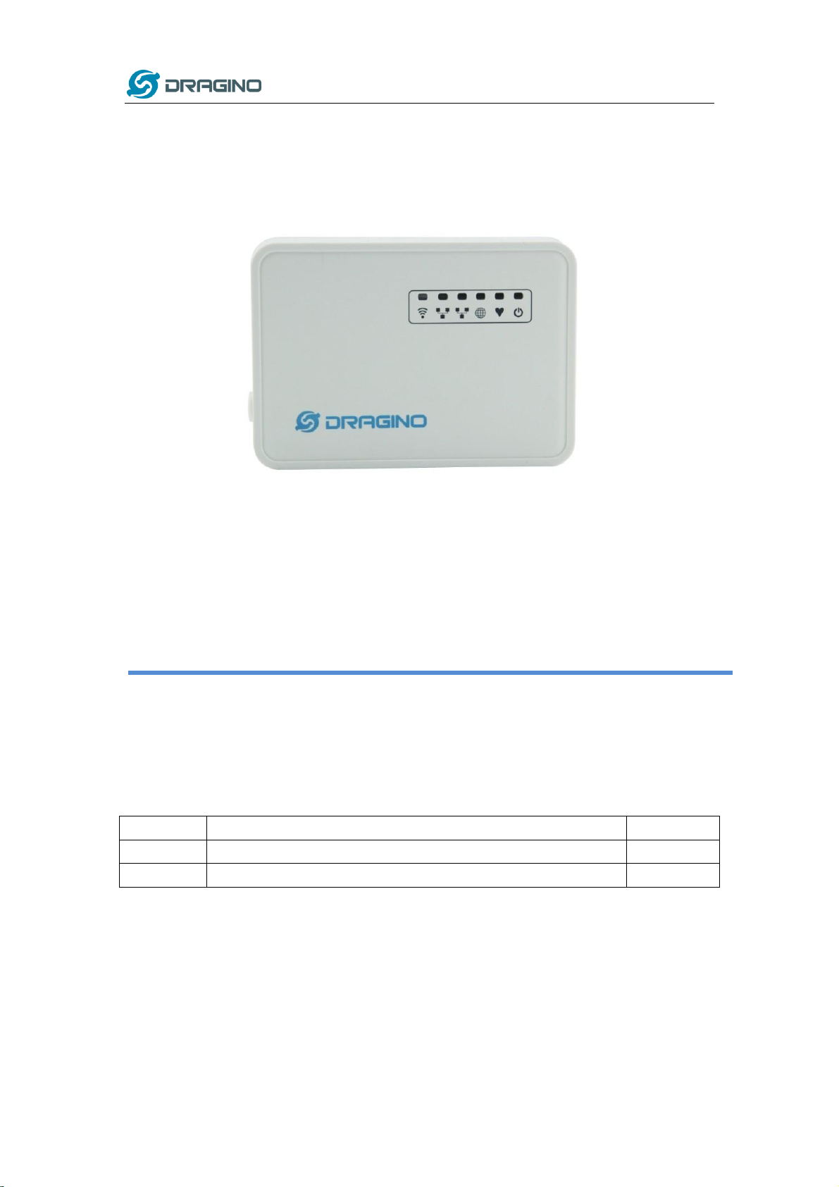
1 Introduction
Software and hardware development guide for Dragino MS14.
2 Software Development Guide
2.1 Access MS14
2.1.1 via console
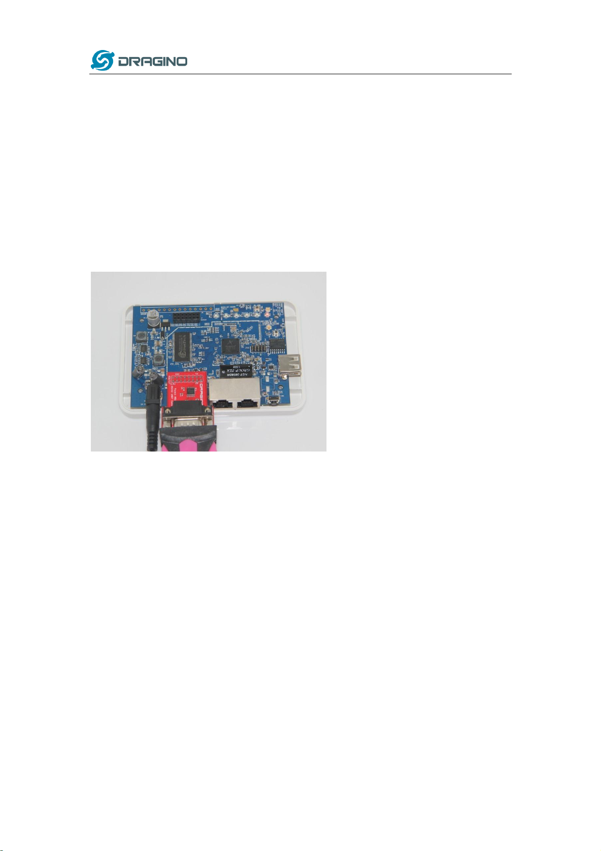
Use the UART module to connect the MS14 as below:
Configure the serial port with below parameters:
Serial: 115200, data: 8bits, Xon/Xoff enable
2.1.2 via SSH
Use SSH to access the LAN port via IP 192.168.255.1
User Name: root
Password: root
ms14 development instruction 3 / 10
Page 4

www.dragino.com
2.2 Compile the firmware
Get source code from Github:
git clone https://github.com/dragino/dragino2.git dragino2
cd into the source directory. Set up build environment,
./set_up_build_enviroment.sh ms14
Build image:
./build_image.sh ms14
to build image for ms14
You should be able to get the firmware in bin directory under image directory.
ms14 development instruction 4 / 10
Page 5

www.dragino.com
2.3 Upgrade firmware
2.3.1 Upgrade firmware in u-boot
Set up your tftp server with ip 192.168.255.2 and put the firmware on tftp server root
//upgrade Kernel
tftp 0x81000000 openwrt-ar71xx-generic-dragino2-kernel.bin
erase 0x9f040000 +0x100000;
cp.b 0x81000000 0x9f040000 $filesize
//upgrade rootfs
tftp 0x81000000 openwrt-ar71xx-generic-dragino2-root-squashfs.bin;
erase 0x9f140000 +0xea0000;
cp.b 0x81000000 0x9f140000 $filesize
2.3.2 Upgrade firmware in OpenWrt
SCP your firmware to the system and then run
root@OpenWrt:~# /sbin/sysupgrade openwrt-ar71xx-generic-dragino2-squashfs-sysupgrade.bin
ms14 development instruction 5 / 10
Page 6

www.dragino.com
2.4 Create your own package
You can create your own package following the instruction in
http://wiki.openwrt.org/doc/devel/packages.
Place the package in source/package directory. And run:
$OPENWRT_PATH/scripts/feeds update
$OPENWRT_PATH/scripts/feeds install -a -p dragino2
To install the package to your openwrt source, remember to use make menuconfig in build dir to
select the package you have created.
Reference: http://wiki.openwrt.org/doc/devel/feeds
2.5 MAC and Unique Key
MAC address:
Each ms14 has been assigned four world-wide unique, continuously MAC address in factory. They
are assigned to
wifi: MAC
eth0: MAC + 2
eth1: MAC +3
The [ MAC+1 ] is reserved for some applications which need two mac in wifi radio.
Unique Key:
A 32 bytes random number generated by TRNG is stored in art partition. Address range is 0x100~
0x11F.
A 2016 bytes random number generated by CSPRNG is stored in art partition, Address range is
0x0120 ~ 0x090F.
Those keys can be used for serial control purpose. To ready them, below is an example command
(assume mtd5 is art partition):
#read 16 bytes key from 0x100
hexdump -v -e '1/1 "%.2x"' -s $((0x100)) -n 16 /dev/mtd5
ms14 development instruction 6 / 10
Page 7
www.dragino.com
Configuration
Power Input
Power Source From
Default(R155 un-populated, R5 un-populated)
9v ~ 15v DC
DC connector
R155 un-populated, R5 populated
9v ~ 15v DC
DC connector, raw_vcc in 2x8 CON
R155 populated, R5 populated
5v DC
DC connector, raw_vcc in 2x8 CON
R155 populated, R5 un-populated
5v DC
DC connector
Pins
Power Output
Comment
VDD33 in 2x8 CON
3.3V
VDD33 in JTAG CON
3.3V VDD5_LDO in 2x8 CON
5V RAW_VCC in 2x8 CON
= raw power input
Only available when R5 is populated.
3 Hardware Development Instruction
3.1 Power option
MS14 provide variously power option for developers.
3.1.1 Power Input
3.1.2 Power Output
ms14 development instruction 7 / 10
Page 8

www.dragino.com
Connector
PIN
Description
2 x 8 ROUTER CON
VDD33
3.3 V power output
VDD5_LDO
5V power output
COLD_RESET
COLD_RESET
GND
GND
GPIO20
GPIO20, SLIC_FS_IN, I2S_SD
GPIO19
GPIO19, SLIC_FS_OUT, I2S_WS
GPIO22
GPIO22, SLIC_DATA_IN, I2S_MICIN
GPIO21
GPIO21, SLIC_DATA_OUT, I2S_MCK
GPIO23
GPIO23, SPDIF_OUT
GPIO18
GPIO18, SLIC_CLK, I2S_CK
GND
GND GPIO24
GPIO24
UART_RX
UART_RX
UART_TX
UART_TX
RAW_VCC
Connect to POWER Input net
SENSOR_LED
Connect to SENSOR_LED, active LOW
2 x 7 ROUTER CON
POS1 ~ POS12
To Sensor OUT screw terminal. With 5V ESD protect
2 x 5 JTAG CON
GPIO26
GPIO26
GPIO27
GPIO27
JTAG_TMS
JTAG_TMS
JTAG_TCK
JTAG_TCK
JTAG_TDI
JTAG_TDI
JTAG_TDO
JTAG_TDO
GPIO15
GPIO15
GPIO16
GPIO16
3.2 Connectors and Pins
3.2.1 Connector Map
3.2.2 COLD_RESET pin
MS14 has a COLD_RESET pin which can reset itself via hardware. This can be used for hardware
watchdog to reset the ms14 in case there is software issue.
The COLD_RESET pin is in the 2x8 connector and active level of this pin is low. Since MS14
already has a pull up resistor for this pin. In the daughter board design, developer only needs to
connect the IO pins from MCU to this COLD_RESET pin directly and control it via daughter board.
ms14 development instruction 8 / 10
Page 9
www.dragino.com
MS14 will enter into reset mode once daughter board send a low level to the COLD_RESET pin, it
will boot again when the low level signal is removed.
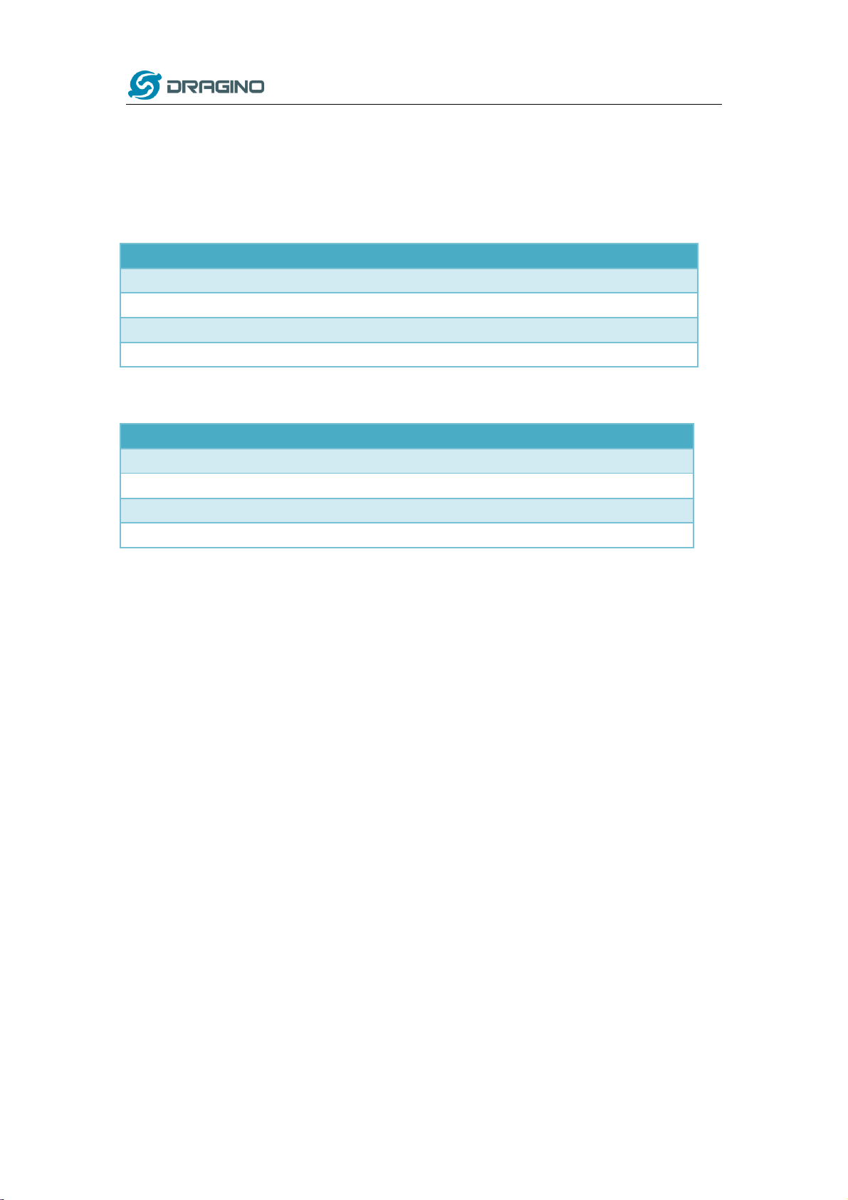
3.3 Antenna and ANT Hole
3.3.1 Antenna
MS14 has two radio paths. They are lead to ANT0 and ANT1. The ANT0 radio is the main antenna
for RX and TX. The ANT1 radio is the diversity antenna for RX only.
By default, MS14 is loaded shipped using 2.5 dB chip antenna. It also provides the option to use
external antenna for higher gain/ directional requirement.
R76 and R77 are path select resistors for main radio path. To use external antenna for main radio
path, developer should remove the 0ohm resister from R77 and solder it on R76. This will disable
ANT0 antenna and enable J4 (i-pex) connector. Then connect the external antenna on J4 and use
it.
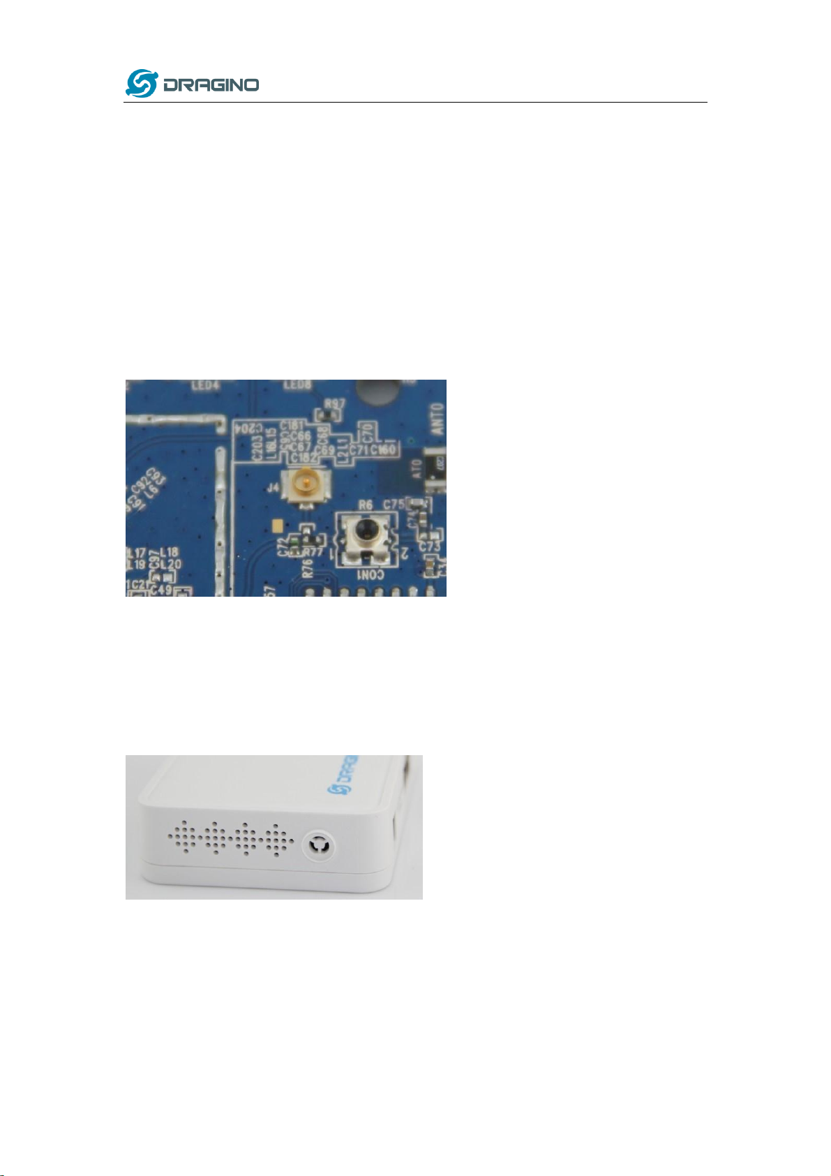
3.3.2 Antenna Hole
The ms14 enclosure has a removable antenna hole which can be used hold the:
External Antenna as mentioned above
Antenna from the daughter board
3.4 Daughter Board Design Clearance
ms14 development instruction 9 / 10
Page 10

www.dragino.com
For PCB design clearance, please refer the file ms14_components_placement. It includes all
components placement and export in 1:1 ratio. Developer can import it to drawing tool such as
Adobe Illustrator to get the exactly dimension to design.
4 Reference
Wiki for MS14
http://wiki.dragino.com/index.php?title=Main_Page#Getting_Start_with_Dragin
o_v2_--_ms14
MS14 Reference Documents:
http://www.dragino.com/downloads/index.php?dir=motherboards/ms14/
SVN Source:
http://svn.dragino.com/dragino2/
ms14 development instruction 10 / 10
 Loading...