

Page 1

Users Manual
A
B
B
B
1
1
1
A
A
1
1
1
2
2
2
6
6
6
Page 2

TABLE OF CONTENTS
TABLE OF CONTENTS .................................................................................................................................... 2
1 System Overview .................................................................................................................................... 3
1.1 General Description ..................................................................................................................... 3
1.2 Features....................................................................................................................................... 3
1.3 Applications.................................................................................................................................. 4
2 Electrical Characteristics..................................................................................................................... 5
2.1 Absolute Maximum Ratings ....................................................................................................... 5
2.2 Recommended Operating Conditions........................................................................................ 5
2.3 Digital Terminals......................................................................................................................... 5
2.4 Reference Clock ........................................................................................................................ 6
2.5 Switching Regulator................................................................................................................... 6
2.6 LDO Regulator........................................................................................................................... 7
2.7 Battery Charger.......................................................................................................................... 7
2.8 Typical Current Consumption..................................................................................................... 7
2.9 Radio Characteristics................................................................................................................. 8
2.9.1 Transmitter ........................................................................................................................ 8
2.9.2 Receiver ............................................................................................................................ 9
3 FCC Statement ..................................................................................................................... 12
................................
Page 3

1 System Overview
1.1 General Description
AB1126 is an optimized single-chip solution which integrates baseband and radio for wireless human input
device applications including 3D glasses, game controller, remote control, and wireless mouse. It complies
with Bluetooth system version 3.0 with the EDR function. AB1126 integrates the Li-ion battery charger circuit
that provides 400mA charging current and reduces customer charging time.
1.2 Features
Compliant with Bluetooth 3.0 specification
Support EDR function
HID profile version 1.1 compliant
3D Sync profile 1.0 compliant
Device ID profile 1.3 compliant
Support 3-axis detection
Support hardware key-scan matrix
Support SPI interface with 2/4-wire mode to mouse sensor IC
Support I2C EEPROM interface
Support UART interface for firmware downloading and peripheral control
Embedded 4 LED drivers with fader
Low cost ROM based design with customer code support
Embedded power management unit
Integrated 1.8V Buck and 1.8/2.7V LDO regulator
Integrated Li-ion battery charger
Single RF port for transmitter and receiver
Receiver sensitivity of -89dBm at basic data rate
Transmit power up to +4dBm with 25 dB gain tuning range
QFN 5mm x 5mm 40 pin package
Page 4
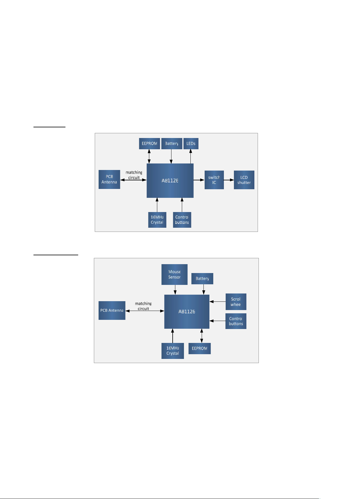
1.3 Applications
There are two typical applications of AB1126. One is 3D Glasses, and the other is wireless mouse. The
application block diagrams are illustrated as below
3D Glasses
Figure 1-1 3DG Application Block Diagram
Wireless Mouse
Figure 1-2 Wireless Mouse Application Block Diagram
Page 5
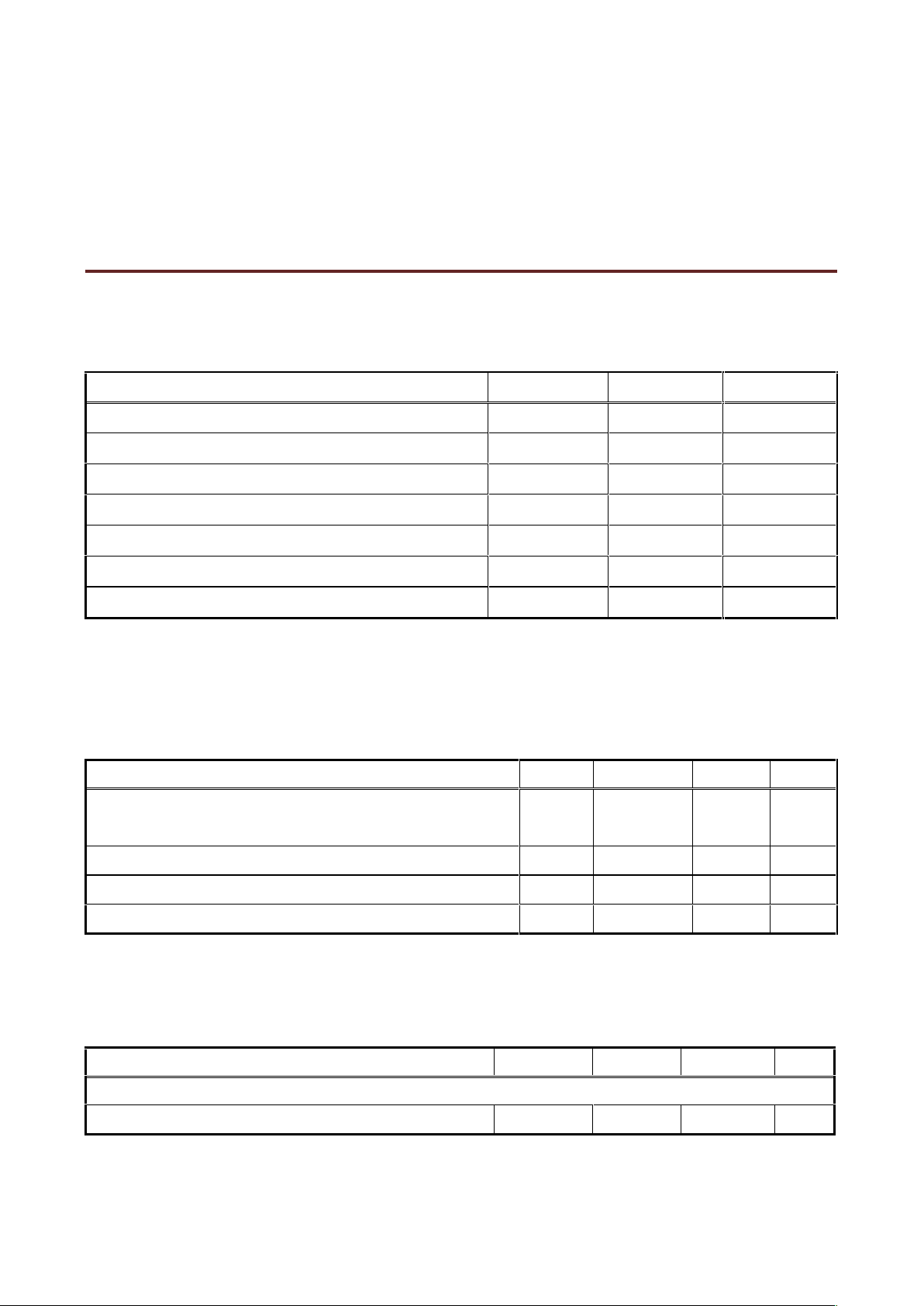
2 Electrical Characteristics
ITEM
MIN.
MAX.
UNIT
I/O supply voltage (VCCIO)
-0.3
5.5
V
Switching Regulator supply voltage (BAT_P)
-0.3
5.5
V
Charger supply voltage (V_CHG)
-0.3
6.5
V
Operating temperature
-40
+85
C
Storage temperature
-65
+150
C
LNA input level
-
+10
dBm
PA output load mismatch
-
10:1
Item
Min.
Typ.
Max.
Unit
Core supply voltage (VCCIF, VCCRF, VCCVCO, VCCPLL,
VCCDIG, VCCXO)
1.8
V
I/O supply voltage (VCCIO)
1.8
3.6
V
Switching Regulator supply voltage (BAT_P)
2
4.2
V
Charger supply voltage (VCHG)
4.556.5
V
Item
Min.
Typ.
Max.
Unit
Input Voltage Levels
Input logic level low (VIL)
0
0.3*VCCIO
V
2.1 Absolute Maximum Ratings
AB1128 could be damaged by any stress in excess of the absolute maximum ratings listed above
Table 3-1 Absolute Maximum Ratings
2.2 Recommended Operating Conditions
2.3 Digital Terminals
Table 3-2 Recommended Operating Conditions
Page 6
Input logic level high (VIH)
0.7*VCCIO
VCCIO+0.4
V
Output Voltage Levels ( VCCIO=1.8V )
Output logic level low (VOL), IO=4.0mA *
0.4
V
Output logic level high (VOH), IO=-4.0mA **
0.7*VCCIO
V
Output Voltage Levels ( VCCIO=3.3V )
Output logic level low (VOL), IO=4.0mA *
0.4
V
Output logic level high (VOH), IO=-4.0mA **
0.7*VCCIO
V
Item
Min.
Typ.
Max.
Unit
Crystal Requirement
Nominal Frequency
16
MHz
Operating Temperature Range
-302585
℃
aging
-20
+20
ppm
Drive level
100
uW
Load capacitance
9
pF
Frequency tolerance
Frequency Stability over Operating Temperature Range
-10
+10
ppm
Crystal Oscillator Characteristics
Tuning Range
-30
+30
ppm
Negative resistance
-150
Ω
Item
Condition
Min.
Typ.
Max.
Unit
Input Voltage
2
4.4
V
Output Voltage
BAT_P > 2.2V
1.7
1.8
1.9
V
Rated Output Current (Iout)
100
mA
Switching Frequency
1.3
MHz
Power Efficiency
@Iout=40mA
90
%
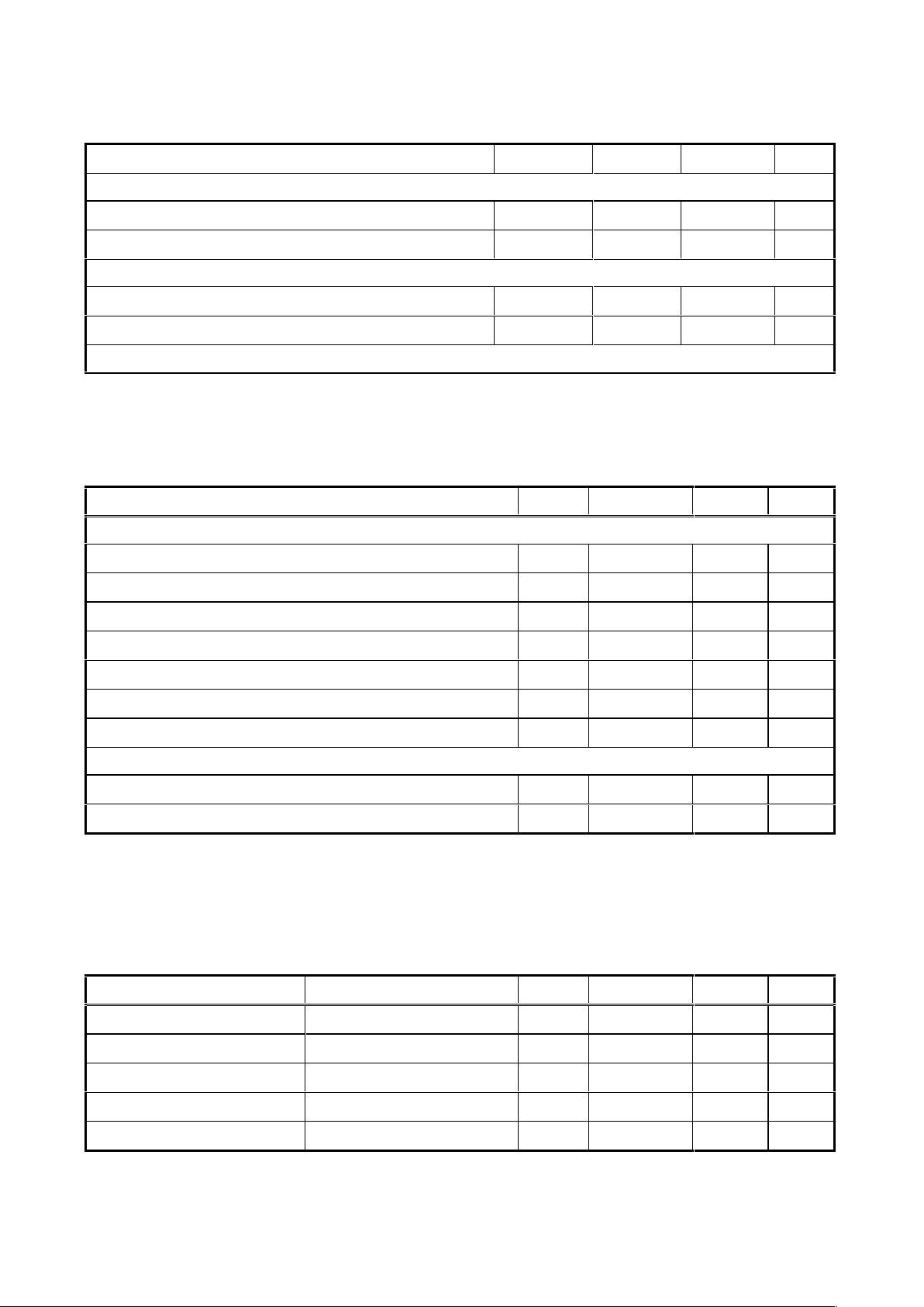
2.4 Reference Clock
Table 3-3 Digital Terminals
Table 3-4 Reference Clock
2.5 Switching Regulator
External inductor = 10uH, External capacitor = 10uF
Page 7
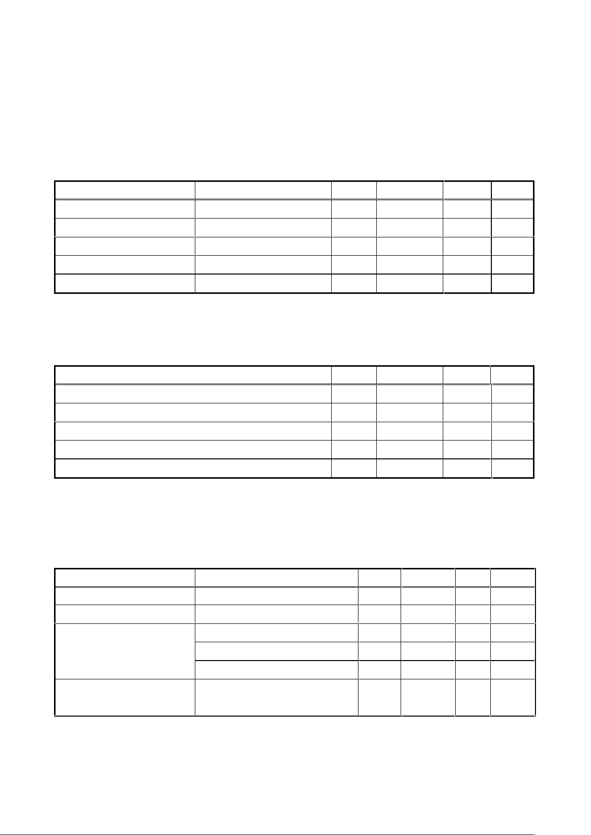
2.6 LDO Regulator
Item
Condition
Min.
Typ.
Max.
Unit
Input Voltage
LI_MODE_N=1
2.0
4.4
V
Input Voltage
LI_MODE_N=0
2.7
4.4
V
Output Voltage
LI_MODE_N=1
1.8
V
Output Voltage
LI_MODE_N=0
2.5
3.2
V
Rated Output Current (Iout)
100
mA
Item
Min.
Typ.
Max.
Unit
Input Voltage
4.556.5
V
Charge Current (CC Mode)
25
400
mA
Trickle Charge Current
8
mA
Trickle to CC Charge Threshold Voltage
3
V
Recharge Battery Hysteresis Voltage
200
mV
Item
Condition
Min.
Typ.
Max.
Unit
Transmit
Peak Current
TBD
mA
Receive
Peak Current
TBD
mA
10 ms
TBD
mA
100 ms
TBD
mA
Sniff mode
1.28 s
TBD
mA
Deep sleep (disconnected, link
loss state, wake on interrupt)
buck off, wake on by all GPIOs
2
uA
External capacitor = 10uF
2.7 Battery Charger
Table 3-5 Switching Regulator
Table 3-6 LDO Regulator
2.8 Typical Current Consumption
Core Supply Voltage = 1.8V (buck output) @ 25℃ unless other specified.
Table 3-7 Battery Charger
Table 3-8 Typical Current Consumption
Page 8
The transmit and the receive current consumptions were measured directly on the buck output (1.8V at 25°C),
Item
Min.
Typ.
Max.
Unit
Maximum RF transmit Power
*1
4
dBm
Maximum RF transmit Power (Low power)
0
dBm
RF power control range
25
dB
20dB bandwidth for modulated carrier
1000
KHz
+2MHz
-20
dBm
-2MHz
-20
dBm
+3MHz
-40
dBm
Adjacent channel transmit
power
-3MHz
-40
dBm
Average deviation in payload
115
KHz
Frequency deviation
Maximum deviation in payload
140
175
KHz
Initial carrier frequency tolerance
-7575KHz
DH1 packet
-2525KHz
DH3 packet
-4040KHz
Drift
DH5 packet
-4040KHz
Drift Rate
-20
20
KHz/50us
Harmonic Content
-45
dBm
Item
Min.
Typ.
Max.
Unit
while the sniff mode and deep sleep current was measured at battery output
2.9 Radio Characteristics
2.9.1 Transmitter
Basic Data Rate
Core Supply Voltage = 1.8V @ 25℃
*1 The maximum RF transmit power could reach 4dBm with appropriate settings
Enhanced Data Rate
Core Supply Voltage = 1.8V @ 25℃
Table 3-9 Transmitter Basic Data Rate
Page 9
Relative transmit power
-1.5
dB
π/4 DQPSK max carrier frequency stability |ωo|
-1010KHz
π/4 DQPSK max carrier frequency stability |ωi|
-7575KHz
π/4 DQPSK max carrier frequency stability |ωo+ωi|
-7575KHz
8DPSK max carrier frequency stability |ωo|
-1010KHz
8DPSK max carrier frequency stability |ωi|
-7575KHz
8DPSK max carrier frequency stability |ωo+ωi|
-7575KHz
RMS DEVM
20
%
99% DEVM
99
%
π/4 DQPSK Modulation Accuracy
Peak DEVM
35
%
RMS DEVM
13
%
99% DEVM
99
%
8DPSK Modulation Accuracy
Peak DEVM
25
%
F > F0 + 3MHz
-40
dBm
F < F0 - 3MHz
-40
dBm
F = F0 + 3MHz
-40
dBm
F = F0 - 3MHz
-40
dBm
F = F0 + 2MHz
-20
dBm
F = F0 - 2MHz
-20
dBm
F = F0 + 1MHz
-26
dBm
In-band spurious emissions
F = F0 - 1MHz
-26
dBm
EDR Differential Phase Encoding
99
%
Item
Min.
Typ.
Max.
Unit
2.402GHz
-89
dBm
2.441GHz
-89
dBm
Sensitivity at 0.1% BER
2.480GHz
-89
dBm
2.402GHz
-84
dBm
Sensitivity at 0.1% BER
(Low Power)
2.441GHz
-84
dBm
2.9.2 Receiver
Basic Data Rate
Core Supply Voltage = 1.8V @ 25℃
Table 3-10 Transceiver Enhanced Data Rate
Page 10
2.480GHz
-84
dBm
Maximum input power at 0.1% BER
-20
dBm
Co-Channel interference
11
dB
F = F0+5MHz
-40
dB
F = F0+4MHz
-40
dB
F = F0+3MHz
-40
dB
F = F0+2MHz
-30
dB
F = F0+1MHz
0
dB
Adjacent channel selectivity
C/I
F = F011
dB
F = F0-1MHz
0
dB
F = F0-2MHz
-20
dB
F = F0-3MHz (F
image
)
-9
dB
F = F0-4MHz
-20
dB
Adjacent channel selectivity
C/I
F = F0-5MHz
-40
dB
Maximum level of intermodulation interference
-39
dBm
30-2000 MHz
-10
dBm
2000-2400 MHz
-27
dBm
2500-3000 MHz
-27
dBm
Blocking @Pin=-67dBm with
0.1%BER
3000-12750 MHZ
-10
dBm
Item
Min.
Typ.
Max.
Unit
π/4 DQPSK
-90
dBm
Sensitivity at 0.01% EDR
8DPSK
-81
dBm
π/4 DQPSK
-86
dBm
Sensitivity at 0.01% EDR
(Low power)
8DPSK
-77
dBm
π/4 DQPSK
-20
dBm
Maximum input power at 0.1%
BER
8DPSK
-20
dBm
π/4 DQPSK
13
dB
Co-Channel interference
8DPSK21dB
π/4 DQPSK
0
dB
Adjacent channel selectivity
C/I
F = F0+1MHz
8DPSK5dB
Enhanced Data Rate
Core Supply Voltage = 1.8V @ 25℃
Table 3-11 Receiver Basic Rate
Page 11
π/4 DQPSK
0
dB
F = F0-1MHz
8DPSK5dB
π/4 DQPSK
-30
dB
F = F0+2MHz
8DPSK
-25
dB
π/4 DQPSK
-20
dB
F = F0-2MHz
8DPSK
-13
dB
π/4 DQPSK
-40
dB
F = F0+3MHz
8DPSK
-33
dB
π/4 DQPSK
-7
dB
F = F
image
8DPSK0dB
Table 3-12 Receiver Enhanced Data Rate
Page 12

FCC STATEMENT :
This device complies with Part 15 of the FCC Rules. Operation is subject to the following
two conditions:
(1) This device may not cause harmful interference, and
(2) This device must accept any interference received, including interference that may
cause undesired operation.
Warning: Changes or modifications not expressly approved by the party responsible for
compliance could void the user's authority to operate the equipment.
NOTE: This equipment has been tested and found to comply with the limits for a Class B
digital device, pursuant to Part 15 of the FCC Rules. These limits are designed to provide
reasonable protection against harmful interference in a residential installation.
This equipment generates uses and can radiate radio frequency energy and, if not
installed and used in accordance with the instructions, may cause harmful interference to
radio communications. However, there is no guarantee that interference will not occur in a
particular installation. If this equipment does cause harmful interference to radio or
television reception, which can be determined by turning the equipment off and on, the
user is encouraged to try to correct the interference by one or more of the following
measures:
Reorient or relocate the receiving an tenna.
Increase the separation between the equipment and receiver.
Connect the equipment into an outlet on a circuit different from that to which the
receiver is connected.
Consult the dealer or an experienced radio/TV technician for help.
RF warning statement:
The device has been evaluated to meet general RF exposure requirement. The device
can be used in portable exposure condition without restriction.
Module Warning Statement:
This Bluetooth module is designed to comply with the FCC statement, FCC ID is: 2ADQG-AB1126.
The host system using this module, should have label in a visible area indicated the following texts:
“Contains FCC ID: 2ADQG-AB1126”.
This radio module must not be installed to co-locate and operated simultaneously with
other radios in host system, additional testing and equipment authorization may be required to
operating simultaneously with other radio.
This Bluetooth module has a PCB antenna. While this module has no shielding, and therefore
the host equipment shall add a shielding function, and any host with module installed, has to be retested,
then additional equipment authorization shall be achieved on the host equipment that has the module installed.
 Loading...