

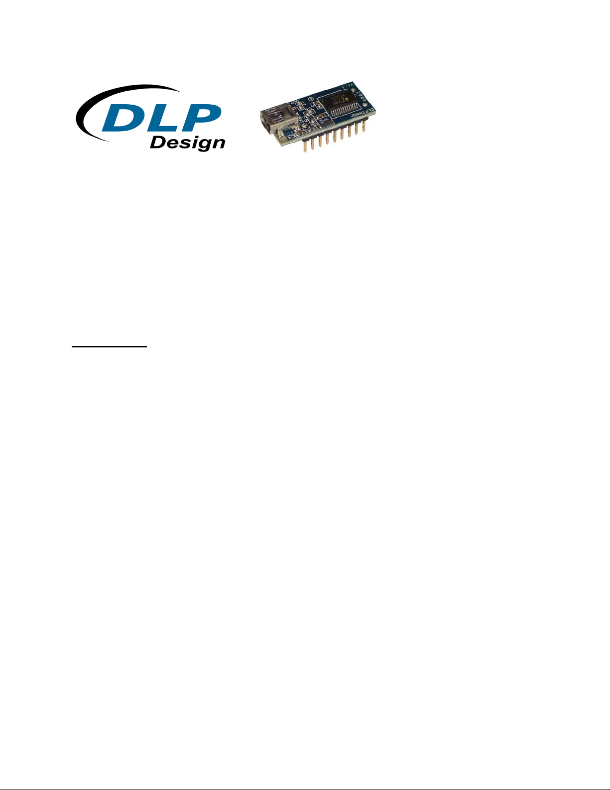
dlp design DLP-USB245R User Manual
DDLLPP-
-
UUSSBB224455RR
LEAD-FREE
UUSSBB--PPAARRAALLLLEELL FFIIFFOO MMoodduullee
The DLP-USB245R is DLP Design’s smallest USB-to-parallel FIFO interface module and
utilizes the popular FT245R IC with FTDIChip-ID™ feature from FTDI. In addition to enabling
standard USB-to-FIFO designs, both asynchronous and synchronous bit-bang interface modes
are also available.
The DLP-USB245R is available in a lead-free, RoHS-compliant, compact 18-pin, 0.1-inch
standard DIP footprint.
FEATURES:
• Single-chip USB-to-parallel FIFO bidirectional data-transfer interface.
• Entire USB protocol handled on the FT245R; no USB-specific firmware programming is
required.
• Fully integrated 1024-bit EEPROM storing device descriptors and FIFO I/O configuration.
• Data transfer rates up to 1Mbyte per second.
• 256-byte receive buffer and 128-byte transmit buffer utilizing buffer-smoothing technology to
allow for high data throughput.
• FTDI’s royalty-free Virtual COM Port (VCP) and direct (D2XX) drivers eliminate the requirement
for USB driver development in most cases.
• Unique USB FTDIChip-ID™ feature.
• Configurable FIFO interface I/O pins.
• Synchronous and asynchronous bit-bang interface options with RD# and WR# strobes.
• Device supplied preprogrammed with a unique USB serial number.
• Supports bus-powered, self-powered and high-power bus-powered USB configurations.
• Integrated level converter on FIFO interface for connection to external logic running at between
+1.8V and +5V.
• True 5V/3.3V/2.8V/1.8V CMOS drive output and TTL input.
• Configurable I/O pin output drive strength.
• Integrated power-on-reset circuit.
• Fully integrated power-supply filtering; no external filtering is required.
• +3.3V to +5.25V single-supply operation.
• Low operating and USB Suspend current.
• UHCI/OHCI/EHCI host-controller compatible.
• USB 2.0 full-speed compatible.
• -40°C to 85°C extended operating temperature range.
Rev. 1.0 (November 2008) 1 © DLP Design, Inc.

APPLICATION AREAS:
• Upgrading legacy peripherals to USB
• Interfacing MCU/PLD/FPGA-based designs to USB
• USB audio and low-bandwidth video data transfer
• PDA-to-USB data transfer
• USB smart card readers
• USB instrumentation
• USB industrial control
• USB MP3 player interface
• USB FLASH card readers and writers
• Set top box PC-USB interface
• USB hardware modems
• USB wireless modems
• USB bar code readers
• USB software and hardware encryption dongles
DRIVER SUPPORT:
Royalty-Free Virtual COM Port (VCP) Drivers for:
• Windows 98, 98SE, ME, 2000, Server 2003, XP and Server 2008
• Windows XP and XP 64-bit
• Windows Vista and Vista 64-bit
• Windows XP Embedded
• Windows CE 4.2, 5.0 and 6.0
• Mac OS 8/9, OS-X
• Linux 2.4 and greater
Royalty-Free D2XX Direct Drivers (USB Drivers + DLL S/W Interface) for:
• Windows 98, 98SE, ME, 2000, Server 2003, XP and Server 2008
• Windows XP and XP 64-bit
• Windows Vista and Vista 64-bit
• Windows XP Embedded
• Windows CE 4.2, 5.0 and 6.0
• Linux 2.4 and greater
The drivers listed above are all available for free download from the DLP Design website
www.dlpdesign.com and FTDI website www.ftdichip.com.
Various third-party drivers are also available for other operating systems; see the FTDI website
www.ftdichip.com for details.
Rev. 1.0 (November 2008) 2 © DLP Design, Inc.

ABSOLUTE MAXIMUM RATINGS
• Storage Temperature -65°C to +150°C
• Ambient Temperature (Power Applied) -40 to +85°C
• VCC Supply Voltage -0.5V to +6.00V
• DC Input Voltage: Inputs -0.5V to VCC + 0.5V
• DC Input Voltage: High-Impedance Bidirectionals -0.5V to VCC + 0.5V
• DC Output Current: Outputs 24mA
D.C. CHARACTERISTICS (AMBIENT TEMPERATURE: -40 TO 85°C)
• VCC Operating-Supply Voltage 4.0 - 5.25V
• VCCIO Operating-Supply Voltage 4.0 - 5.25V
• Operating Supply Current 15mA (Normal Operation)
• Operating Supply Current 100uA USB Suspend
1.0 GENERAL DESCRIPTION
The DLP-USB245M provides an easy, cost-effective method of transferring data to/from a
peripheral and a host at up to 8 million bits (1 megabyte) per second. Its simple, FIFO-like
design makes it easy to interface to any microcontroller or microprocessor via I/O ports.
To send data from the peripheral to the host computer, simply write the byte-wide data into the
module when TXE# is low. If the (128-byte) transmit buffer fills up or is busy storing the
previously-written byte, the device takes TXE# high in order to stop further data from being
written until some of the FIFO data has been transferred over USB to the host.
When the host sends data to the peripheral over USB, the device will take RXF# low to let the
peripheral know that at least one byte of data is available. The peripheral then reads the data
until RXF# goes high, thereby indicating that no more data is available to be read.
By using FTDI’s Virtual COM Port drivers, the peripheral looks like a standard COM port to the
application software. Commands to set the baud rate are ignored; the device always transfers
data at its fastest rate regardless of the application’s baud-rate setting. The latest versions of
the drivers are available for download from DLP Design’s website at www.dlpdesign.com.
Rev. 1.0 (November 2008) 3 © DLP Design, Inc.
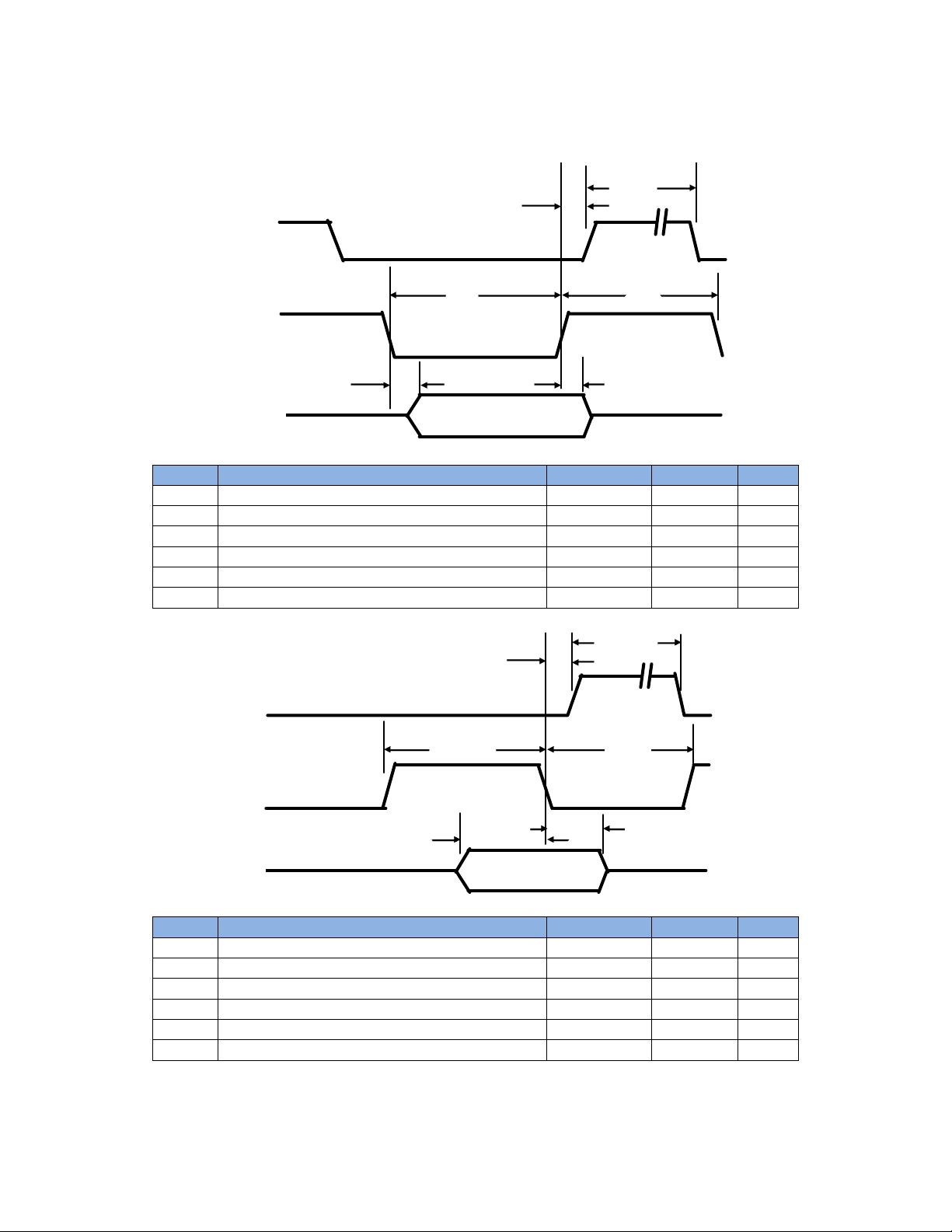
2.0 TIMING DIAGRAMS
T5
RXF#
RD#
D[7..0]
D
Desc riptio n Min Max U nit
TTIIMMEE DDEESSCCRRIIPPTTIIOONN
T1
T2
T3
T4
T5
T6
*Load = 30pF
RD# Active Pulse Width
RD# to RD# Pre-Charge Time
RD# Active to Valid Data*
Valid Data Hold Time from RD# Inactive*
RD# Inactive to RXF#
RXF# Inactive After RD Cycle
TXE#
WR
TTIIMMEE DDEESSCCRRIIPPTTIIOONN
T7
T8
T9
T10
T11
T12
*Load = 30pF
WR Active Pulse Width
WR to WR Pre-Charge Time
Valid Data Setup to WR Falling Edge*
Valid Data Hold Time from WR Inactive*
WR Inactive to TXE#
TXE# Inactive After WR Cycle
T6
T1 T2
T3 T4
Valid data
MMIIN
N
50 - nS
50 + T6 - nS
20 50 nS
0 - nS
0 25 nS
80 - nS
MMIIN
T12
T8
N
T11
T7
T9
Va lid dat aD[7..0]
50 - nS
50 - nS
20 - nS
0 - nS
5 25 nS
80 - nS
MMAAXX UUNNIIT
T10
MMAAXX UUNNIIT
T
T
Rev. 1.0 (November 2008) 4 © DLP Design, Inc.
 Loading...