

DIZIC DZZBSP User Manual
DZ-ZB-SP IEEE 802.15.4/ZigBee RF Module
Quickly add wireless communication with these high performances modules
The DiZiC DZ-ZB-SP 802.15.4 Module allows you to
quickly add wireless networking capabilities to your
products. These ZigBee-compliant modules are ready-
to-use, simple to operate, and available in a wide
range of configurations. They are ideal for industrial
sensors, consumer remote controls, home appliances,
and more.
Compact Form Factor – With 30 mm by 19 mm, this
module can be shielded for enhanced EMI protection.
DZ-ZB-SP Module with Shield
Complete System-on-Module
• 2.4 GHz CSS transceiver
• 32-bit ARM® Cortex-M3 processor
• 128 kB flash, 8kB RAM memory
• AES128 encryption accelerator
• Flexible ADC, UART serial communication, and
general purpose timers
• Highly configurable GPIO with Schmitt trigger inputs
Industry-leading ARM Cortex-M3 processor
• Leading 32-bit processing performance
• Highly efficient Thumb-2 instruction set
• Operation at 6, 12 or 24 MHz
• Flexible Nested Vectored Interrupt Controller
Innovative network and processor
debug
• Serial Wire Debug interface
• Standard ARM debug capabilities:
Flash Patch &Breakpoint; Data Watch-point & Trace
RF Performances
• Rx sensitivity (- 100 dBm)
• Tx output power level (+8 dBm)
Low power consumption, advanced
management
• RX Current (w/ CPU): 27 mA
• TX Current (w/ CPU, +3dBm) 31 mA
• Low deep sleep current, less than 400nA
• Low-frequency internal RC oscillator for lowpower sleep timing
• High-frequency internal RC oscillator for fast
(100 usec) processor start-up from sleep
Target Applications
• Smart Energy
• Building automation and control (HVAC)
• Home automation and control
• Security and monitoring
• AMR/AMI
• Medical
• General ZigBee wireless sensor networking
• Wireless hand-held terminals
• Industry telemetry /automatic data
collection
• Temperature and humidity control systems

Table of Content
1. Product Approvals....................................................................................................................................... 4
1.1. FCC Approvals...................................................................................................................................... 4
1.2. IC (Industry Canada) Approvals............................................................................................................ 4
1.3. European Certification (ETSI)............................................................................................................... 5
2. Configuration.............................................................................................................................................. 6
2.1. Power Level Option [S]......................................................................................................................... 6
2.2. RF Output Options: Codes [P], [I] or [E] .............................................................................................. 6
2.3. Protocol Stack Options: Codes [F], [X] or [Z] ...................................................................................... 6
2.4. EMI Protection Options: Codes [M] or [].............................................................................................. 6
3. Block Diagram............................................................................................................................................ 7
4. Absolute Maximum Rating......................................................................................................................... 8
4.1. Voltage Characteristics.......................................................................................................................... 8
4.2. Current Characteristics.......................................................................................................................... 8
4.3. Thermal Characteristics......................................................................................................................... 8
5. Components ................................................................................................................................................ 9
5.1. STM32W108 –System-on-Chip Transceiver ........................................................................................ 9
5.1.1. IEEE802.15.4 Compliant Transceiver............................................................................................... 9
5.1.2. Operation Modes............................................................................................................................... 9
5.1.3. Flash and RAM Memory................................................................................................................. 10
5.1.4. Integrated MAC Functions.............................................................................................................. 10
5.1.5. Power Management......................................................................................................................... 10
5.1.6. Peripherals....................................................................................................................................... 10
5.1.7. Interfaces......................................................................................................................................... 10
5.2. Protocol Stacks.................................................................................................................................... 11
6. Electrical Characteristics........................................................................................................................... 12
6.1. Parameter conditions........................................................................................................................... 12
6.1.1. Minimum and Maximum Values.................................................................................................... 12
6.1.2. Typical values ................................................................................................................................. 12
6.2. Operating Conditions........................................................................................................................... 12
6.2.1. General Operating Conditions......................................................................................................... 12
6.2.2. Electrostatic Discharge (ESD)......................................................................................................... 13
6.2.3. DC Characteristics .......................................................................................................................... 13
6.3. RF Characteristic................................................................................................................................. 15
6.3.1. Receiver Characteristics.................................................................................................................. 15
6.3.2. Transmitter Characteristics ....................................................................................................................... 15
7. Mechanical Characteristics ....................................................................................................................... 16
7.1. Module Pad Diagram........................................................................................................................... 16
7.2. Module Pads........................................................................................................................................ 16
7.3. Module Mechanical Dimensions......................................................................................................... 23
8. Soldering................................................................................................................................................... 24
8.1. Soldering (Reflow) Profile .................................................................................................................. 24
8.2. Profile Parameters................................................................................................................................ 24
8.3. Recommended Footprint ..................................................................................................................... 25
9. References................................................................................................................................................. 26
Document Information.......................................................................................................................................... 27
Revision History ................................................................................................................................................... 27
About DiZiC ......................................................................................................................................................... 27
October 2012 Doc ID:DZ DS-ZBSP MOD rev1.0
© 2012 DiZiC Co. Ltd. Subject to change without notice.
2

Table of Figures
Fig. 1 Simplified Block Diagram of the Module..................................................................................................... 7
Fig. 2 Block diagram of System-on-Chip STM32W108.........................................................................................9
Fig. 3 Available protocol stacks............................................................................................................................ 11
Fig. 4 Pad connection diagram for modules (top view)........................................................................... ............. 16
Fig. 5 Standard module dimensions with metal shielding..................................................................................... 23
Fig. 6 Recommended Temperature Profile for Soldering (Reflow)...................................................................... 24
Fig. 7 Recommended Footprint for Module.......................................................................................................... 25
Fig. 8 Recommended Footprint for Module.......................................................................................................... 25
List of Tables
Table 1: Power level option .................................................................................................................................... 6
Table 2: Output options........................................................................................................................................... 6
Table 3: Protocol stack options............................................................................................................................... 6
Table 4: EMI protection options............................................................................................................................. 6
Table 5: Voltage characteristics.............................................................................................................................. 8
Table 6: Current characteristics .............................................................................................................................. 8
Table 7: Thermal characteristics............................................................................................................................. 8
Table 8: General operating conditions.................................................................................................................. 12
Table 9: ESD absolute maximum ......................................................................................................................... 13
Table 10: DC electrical characteristics.................................................................................................................. 14
Table 11: Receiver characteristics......................................................................................................................... 15
Table 12: Transmitter characteristics.................................................................................................................... 15
Table 13: Pad description...................................................................................................................................... 22
Table 14: Solder Reflow Parameters..................................................................................................................... 24
October 2012 Doc ID:DZ DS-ZBSP MOD rev1.0
© 2012 DiZiC Co. Ltd. Subject to change without notice.
3

1. Product Approvals
The DZ-ZB-SP has been designed to meet all national regulations for world-wide use.
The transmitter module may not be co-located with any other transmitter or antenna.
Please be advised that DiZiC Co., Ltd. declares that the DZ-ZB-G module will be used exclusively by
OEM’s or ODM’s and will therefore not be directly accessible by end users.
1.1. FCC Approvals
The DZ-ZB-SP with PCB Antenna has been tested to comply with FCC CFR Part 15 (USA) The
devices meet the requirements for modular transmitter approval as detailed in the FCC public notice
DA00.1407.transmitter.
FCC statement:
This device complies with Part 15 of the FCC rules. Operation is subject to the following two
conditions: (1) this device may not cause harmful interference, and (2) this device must accept any
interference received, including interference that may cause undesired operation.
FCC ID: YCMDZZBSP
The FCC requires the user to be notified that any changes or modifications made to this device that
are not expressly approved by the manufacturer may void the user's authority to operate the
equipment.
FCC Labeling Requirements
When integrating the DZ-ZB-SP into a product it must be ensured that the FCC labeling requirements
are met. This includes a clearly visible label on the outside of the finished product specifying the DiZiC
FCC identifier (FCC ID: YCMDZZBSP) as well as the FCC notice shown on the previous page. This
exterior label can use wording such as "Contains Transmitter Module FCC ID: YCMDZZBSP “ or
"Contains FCC ID: YCMDZZBSP " although any similar wording that expresses the same meaning
may be used.
1.2. IC (Industry Canada) Approvals
The DZ-ZB-SP with integrated Antenna has been tested to comply with IC.
IC-ID: 9022A- DZZBSP
The labeling requirements for Industry Canada are similar to those of the FCC. Again, a clearly visibly
label must be placed on the outside of the finished product stating something like "Contains
Transmitter Module, IC: 9022A- DZZBSP ", although any similar wording that expresses the same
meaning may be used.
IC (Industry Canada) statement:
This module complies with Industry Canada RF radiation exposure limits set forth for general
population/uncontrolled environment. This device complies with Industry Canada licence-exempt RSS
standard(s).Operation is subject to the following two conditions: (1) this device may not cause
interference, and (2) this device must accept any interference, including interference that may cause
undesired operation of the device.
The integrator is responsible for the final product to comply to IC ICES-003 and FCC Part 15, Sub. B Unintentional Radiators.
October 2012 Doc ID:DZ DS-ZBSP MOD rev1.0
© 2012 DiZiC Co. Ltd. Subject to change without notice.
4

1.3. European Certification (ETSI)
The DZ-ZB-SP has been certified to the following standards:
Radio: EN 300 328:V1.7.1
EMC: EN 301 489-17:V2.1.1
Safety: EN 60950-1:2005 (Ed. 2.0)
If the DZ-ZB-SP module is incorporated into an OEM product, the OEM product manufacturer must
ensure compliance of the final product to the European Harmonized EMC, and low voltage/ safety
standards. A Declaration of Conformity must be issued for each of these standards and kept on file as
described in Annex II of the R&TTE Directive. The final product must not exceed the specified power
ratings, antenna specifications and installation requirements as specified in this user manual. If any of
these specifications are exceeded in the final product then a submission must be made to a notified
body for compliance testing to all of the required standards.
The 'CE' marking must be applied to a visible location on any OEM product. For more information
please refer to http://ec.europa.eu/enterprise/faq/ce-mark.htm. Customers assume full responsibility
for learning and meeting the required guidelines for each country in their distribution market.
.
October 2012 Doc ID:DZ DS-ZBSP MOD rev1.0
© 2012 DiZiC Co. Ltd. Subject to change without notice.
5
2. Configuration
The module comes with different configuration options. RF Output Options, Protocol Stack Options,
and EMI Protection Options.
2.1. Power Level Option [S]
The module DZ-ZB-S has the power option S preselected.
Selector Options Description
STM32W chip: System on Chip - where radio, microcon-
[S] Standard +8dBm
Table 1: Power level option
2.2. RF Output Options: Codes [P], [I] or [E]
Three RF output options are available, including an onboard PCB antenna or a U.FL connector.
Selector Options Description
[P] Embedded PCB Antenna
[I] I-PEX / U.FL connector
[E] External +2dBi dipole Antenna
Table 2: Output options
troller, program/user memory, RAM, ZigBee protocols
stack are integrated in one chi
2.3. Protocol Stack Options: Codes [F], [X] or [Z]
Three protocol stack options are available, including an RF4CE stack, a Zigbee Pro stack from Ember,
and a proprietary MAC/Phy stack
Selector Options Description
[F] RF4CE stack
[X] Proprietary stack
[Z] EmberZnet PRO stack
Table 3: Protocol stack options
2.4. EMI Protection Options: Codes [M] or []
A metal shield cap can be added to the module for EMI protection.
Selector Options Description
[M] Metal shield cap
[ ] Standard module RF Module without metal shielding
Table 4: EMI protection options
Enables enhanced level of electromagnetic immunity
(EMI) protection.
October 2012 Doc ID:DZ DS-ZBSP MOD rev1.0
© 2012 DiZiC Co. Ltd. Subject to change without notice.
6
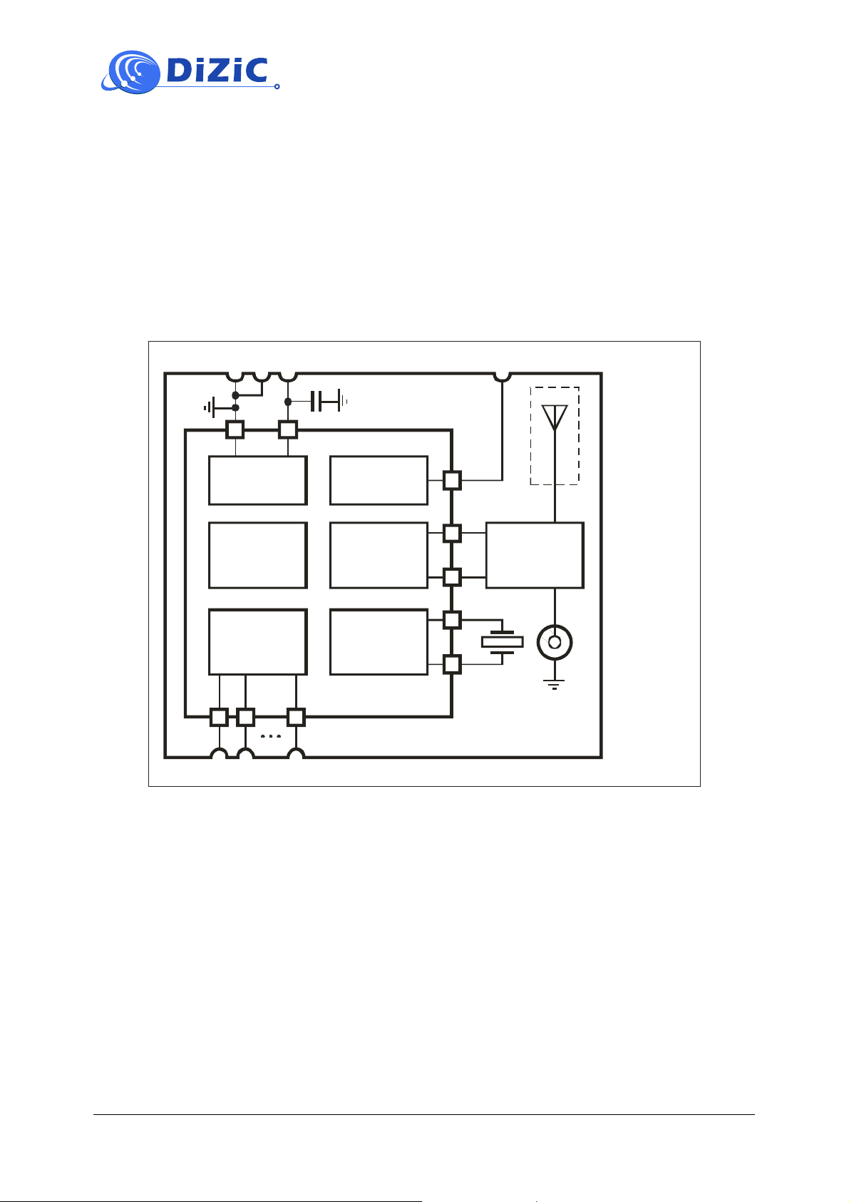
3. Block Diagram
The DZ-ZB Module is low-power, highly sensitivity IEEE 802.15.4 / ZigBee-compliant module. This
multi-functional device is based on the STMicroelectronics STM32W108 fully integrated System-onChip [1] (STM32W108CBU6x version).
This STM32W108 SoC integrates a 2.4 GHz IEEE 802.15.4-compliant transceiver, a 32-bit ARM®
Cortex™- M3 microprocessor, Flash and RAM memory, as well as peripherals for use by designers of
ZigBee-based systems [2]
nRESETVSS VCC
Output
Options:
Embedded
PCB
Antenna
Power
Manager
Decoupling
Power On
Reset
MAC and
Baseband
GPIO / ADC
Timers
other periph.
RF
Transceiver
Crystal
Oscillator
Impedance
Matching
Network
50 Ohm
U.FL Coax
Connector
STM32W108
DZ-ZB-P-O-S-E
GPIO
Fig. 1 Simplified Block Diagram of the Module
October 2012 Doc ID:DZ DS-ZBSP MOD rev1.0
© 2012 DiZiC Co. Ltd. Subject to change without notice.
7
4. Absolute Maximum Rating
Stresses above the absolute maximum ratings listed in this section may cause permanent damage to
the device. These are stress ratings only and functional operation of the device at these conditions is
not implied. Exposure to maximum rating conditions for extended periods may affect device reliability
4.1. Voltage Characteristics
Ratings Min. Max. Unit
VCC input voltage (VDD_PADS) -0.3 +3.6 V
RF Input Power (for max level for correct packet reception
Receive characteristics) RX signal input
Voltage on any GPIO (PA[7:0], PB[7:0], PC[7:0]), SWCLK,
nRESET
Table 5: Voltage characteristics
15 dBm
-0.3
VDD_PADS
+0.3
V
4.2. Current Characteristics
Symbol Ratings Max. Unit
IVDD Total current into VDD/VDDA power lines (source) 150 mA
IVSS Total current out of VSS ground lines (sink) 150 mA
IIO Output current sunk by any I/O and control pin 25 mA
Table 6: Current characteristics
4.3. Thermal Characteristics
Symbol Ratings Value Unit
TSTG Storage temperature range -40 to +85 °C
TJ Maximum junction temperature 150 °C
Table 7: Thermal characteristics
October 2012 Doc ID:DZ DS-ZBSP MOD rev1.0
© 2012 DiZiC Co. Ltd. Subject to change without notice.
8
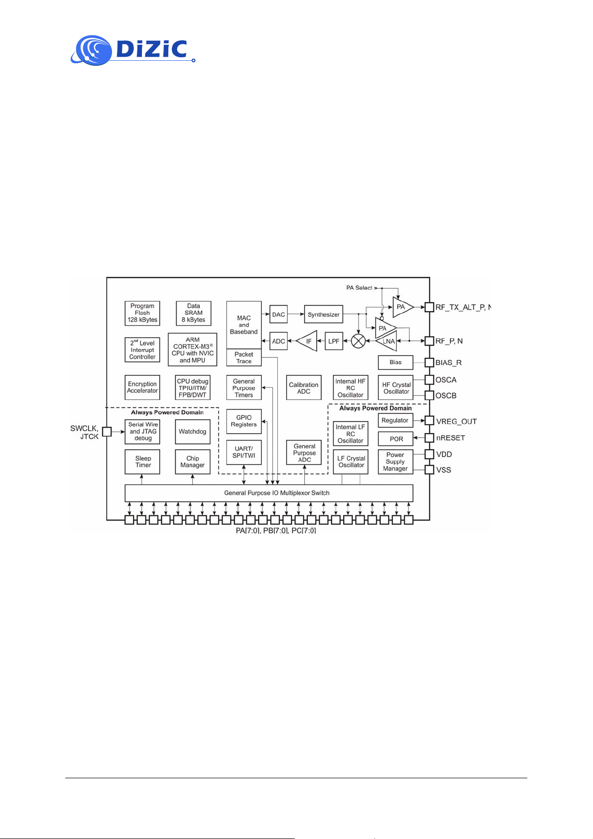
5. Components
This section describes the key components of the DZ-ZB Module including the STM32W108 SoC, the
RF Front End, and the protocol stacks.
5.1. STM32W108 –System-on-Chip Transceiver
The STM32W108 is a fully integrated System-on-Chip that includes:
2.4 GHz, IEEE 802.15.4 compliant transceiver
32-bit ARM® Cortex™ -M3 microprocessor
Flash and RAM memory
Peripherals for use of designers of ZigBee-based systems
Fig. 2 Block diagram of System-on-Chip STM32W108
5.1.1. IEEE802.15.4 Compliant Transceiver
This SoC transceiver utilizes an efficient architecture that exceeds the dynamic range requirements
imposed by the IEEE 802.15.4-2003 standard by over 15 dB. The integrated receive channel filtering
allows for robust co-existence with other communication standards in the 2.4 GHz spectrum such as
IEEE 802.11 and Bluetooth. The integrated regulator, VCO, loop filter, and power amplifier keep the
external component count low. An optional high performance radio mode (boost mode) is softwareselectable to boost dynamic range.
5.1.2. Operation Modes
The integrated 32-bit ARM® Cortex™-M3 microprocessor is highly optimized for high performance,
low power consumption, and efficient memory utilization. With its integrated MPU, the STM32W108
supports two different modes of operation: System mode and Application mode.
October 2012 Doc ID:DZ DS-ZBSP MOD rev1.0
© 2012 DiZiC Co. Ltd. Subject to change without notice.
9
 Loading...