

DIZIC DZZBSA User Manual

802.15.4 Family of RF Modules
High Performance and Long Range
DiZiC 802.15.4 DZ-ZB RF Modules
Quickly add wireless capability with these high performance ZigBee compliant modules
The DiZiC DZ-ZB 802.15.4 Modules allow you to quickly
add wireless networking capabilities to your products.
These ZigBee-compliant modules are ready-to-use,
simple to operate, and available in a wide range of
configurations. They are ideal for industrial sensors,
consumer remote controls, home appliances, and more.
Features
+
STM32W108 ZigBee / IEEE 802.15.4 SoC
• Complete System-on-Chip
• 32-bit ARM® Cortex-M3 processor
• 2.4 GHz IEEE 802.15.4 transceiver & lower MAC
• Supports 16 channels
• 128 kB flash, 8 kB SRAM memory
• 128-bit AES encryption accelerator
• Flexible ADC, SPI/UART/TWI serial communications,
and general purpose timers
• 24 highly configurable GPIO with Schmitt trigger
inputs
• Data rate up to 250 kbit/s
+
Low power consumption, advanced management:
• RX Current (w/ CPU): 27 mA
• TX Current (w/ CPU, +3 dBm TX): 31 mA
• Low deep sleep current with retained RAM and
GPIO:
400 nA/ 800 nA with/without sleep timer
• Low-frequency internal RC oscillator for low-power
sleep timing
• High-frequency internal RC oscillator for fast (100
µsec) processor start-up from sleep
+
Innovative network and processor debug:
• Serial Wire/JTAG interface
• Standard ARM debug capabilities: Flash Patch &
Breakpoint; Data Watch-point & Trace; Instrumentation Trace Macrocell
+
Exceptional RF Performance
• Normal mode Link Budget up to 102 dB; configurable
up to107 dB
• -99 dBm normal RX sensitivity; configurable to -100
dBm (1%PER, 20 byte packet)
• +3 dB normal mode output power; configurable up to
+7 dBm
• Robust WiFi and Bluetooth coexistence
+
Application Flexibility:
• Single voltage operation: 2.1 V to 3.6 V
• Optional 32.768 kHz crystal for higher timer
accuracy
• Low external component count with single 24 MHz
crystal
• External power amplifier versions
+
Peripherals
• 24 GPIOs, SPI, USART, and I2C
• 12-bit ADC with up to 6 inputs
• 2x 16-bit timers
• DMA controller
+
Power Level Options:
• standard power level (+7 dBm)
• Or two RF Front End (PA and LNA, +20 dBm) versions.
+
RF Output Options:
• Chip antenna
• U.FL connector
• Single port 50 Ohm RF pad.
+
ZigBee Software Stack Options:
• EmberZNet PRO ZigBee stack
• RF4CE stack
• Low level PHY / MAC stack.
+
EMI Options:
• Standard version without shielding
• Metal shielding protection
Target Applications
• Smart Energy
• Building automation and control (HVAC)
• Home automation and control
• Security and monitoring
• AMR/AMI
• Logistic & Asset tracking
• Medical
• General ZigBee wireless sensor networking
• Active RFID
• Wireless hand-held terminals
• Industry telemetry /automatic data collection
• Temperature and humidity control systems
• Traffic and control for street lamp
July 2010 Doc ID: PB-ZB-MOD-003-20DS Page i
© 2010 DiZiC Co. Ltd. Subject to change without notice.

Table of Contents
DiZiC 802.15.4 DZ-ZB RF Modules
Table of Contents
List of Tables ..................................................................................................................................................................... iii
List of Figures ................................................................................................................................................................... iv
1. Product Approvals ........................................................................................................................................................ 1
1.1. FCC Approvals ....................................................................................................................................................... 1
1.2. IC (Industry Canada) Approvals ............................................................................................................................. 1
1.3. European Certification (ETSI) ................................................................................................................................ 1
2. Configurations .............................................................................................................................................................. 3
2.1. Power Level Options: Codes [S] [R] or [T] ............................................................................................................. 4
2.2. RF Output Options: Codes [A] [P] or [U] ................................................................................................................ 4
2.3. ZigBee Stack Options: Codes [F] [X] or [Z] ............................................................................................................ 4
2.4. EMI Protection Options: [M] or [S] .......................................................................................................................... 5
2.5. Configuration Options Matrix .................................................................................................................................. 5
3. Block Diagram ............................................................................................................................................................... 7
4. Absolute Maximum Ratings ......................................................................................................................................... 8
4.1. Voltage Characteristics .......................................................................................................................................... 8
4.2. Current Characteristics .......................................................................................................................................... 8
4.3. Thermal Characteristics ......................................................................................................................................... 8
5. Components .................................................................................................................................................................. 9
5.1. STM32W108 – System-on-Chip Transceiver ......................................................................................................... 9
5.2.1. IEEE 802.15.4 Compliant Transceiver ........................................................................................................... 9
5.3.2. Operation Modes.......................................................................................................................................... 10
5.4.3. Flash and RAM Memory............................................................................................................................... 10
5.5.4. Integrated MAC Functions............................................................................................................................ 10
5.6.5. Power Management ..................................................................................................................................... 10
5.7.6. Peripherals ................................................................................................................................................... 10
5.8.7. Interfaces...................................................................................................................................................... 10
5.9. + 20 dBm Front End (PA and LNA) with RF Output Power Level Detector ......................................................... 11
5.10. + 20 dBm RF Front End Front End (PA and LNA) ............................................................................................. 12
5.11. ZigBee Stacks .................................................................................................................................................... 13
6. Electrical Characteristics ........................................................................................................................................... 15
6.1. Parameter conditions ........................................................................................................................................... 15
6.2.1. Minimum and Maximum Values ................................................................................................................... 15
6.3.2. Typical values............................................................................................................................................... 15
6.4. Operating Conditions ........................................................................................................................................... 15
6.5.1. General Operating Conditions...................................................................................................................... 15
6.6.2. Electrostatic Discharge (ESD)...................................................................................................................... 15
6.7.3. DC Characteristics ....................................................................................................................................... 16
6.8. RF Characteristic ................................................................................................................................................. 18
6.9.1. Receiver Characteristics .............................................................................................................................. 18
6.10.2. Transmitter Characteristics ........................................................................................................................ 19
7. Mechanical Characteristics ....................................................................................................................................... 21
7.1. Module Pad Diagram ........................................................................................................................................... 21
7.2. Module Pads ........................................................................................................................................................ 21
7.3. Package Mechanical Dimensions ........................................................................................................................ 30
8. Soldering ..................................................................................................................................................................... 33
8.1. Solder Temperature Profile .................................................................................................................................. 33
8.2.1. Reflow Profile ............................................................................................................................................... 33
8.3. Profile Parameters ............................................................................................................................................... 33
8.4. Recommended Footprint ...................................................................................................................................... 34
9. Ordering Information .................................................................................................................................................. 36
10. Acronyms .................................................................................................................................................................. 37
11. References ................................................................................................................................................................ 39
July 2010 Doc ID: PB-ZB-MOD-003-20DS Page ii
© 2010 DiZiC Co. Ltd. Subject to change without notice.

List of Tables
DiZiC 802.15.4 DZ-ZB RF Modules
List of Tables
Table 1: Power level options . . . . . . . . . . . . . . . . . . . . . . . . . . . . . . . . . . . . . . . . . . . . . . . . . . . . . . . . . . . . . . . . . . . . . . . 4
Table 2: Output Options . . . . . . . . . . . . . . . . . . . . . . . . . . . . . . . . . . . . . . . . . . . . . . . . . . . . . . . . . . . . . . . . . . . . . . . . . . . 4
Table 3: ZigBee Stack Options . . . . . . . . . . . . . . . . . . . . . . . . . . . . . . . . . . . . . . . . . . . . . . . . . . . . . . . . . . . . . . . . . . . . . 4
Table 4: SEMI Protection Options . . . . . . . . . . . . . . . . . . . . . . . . . . . . . . . . . . . . . . . . . . . . . . . . . . . . . . . . . . . . . . . . . . . 5
Table 5: DZ-ZB module options set . . . . . . . . . . . . . . . . . . . . . . . . . . . . . . . . . . . . . . . . . . . . . . . . . . . . . . . . . . . . . . . . . . 5
Table 6: Configuration options matrix . . . . . . . . . . . . . . . . . . . . . . . . . . . . . . . . . . . . . . . . . . . . . . . . . . . . . . . . . . . . . . . . 5
Table 7: Voltage characteristics . . . . . . . . . . . . . . . . . . . . . . . . . . . . . . . . . . . . . . . . . . . . . . . . . . . . . . . . . . . . . . . . . . . . . 8
Table 8: Current characteristics . . . . . . . . . . . . . . . . . . . . . . . . . . . . . . . . . . . . . . . . . . . . . . . . . . . . . . . . . . . . . . . . . . . . . 8
Table 9: Thermal characteristics . . . . . . . . . . . . . . . . . . . . . . . . . . . . . . . . . . . . . . . . . . . . . . . . . . . . . . . . . . . . . . . . . . . . 8
Table 10: Functional description of the Front End signals . . . . . . . . . . . . . . . . . . . . . . . . . . . . . . . . . . . . . . . . . . . . . . . . 11
Table 11: Functional description of the Front End signals . . . . . . . . . . . . . . . . . . . . . . . . . . . . . . . . . . . . . . . . . . . . . . . . 13
Table 12: General operating conditions . . . . . . . . . . . . . . . . . . . . . . . . . . . . . . . . . . . . . . . . . . . . . . . . . . . . . . . . . . . . . . 15
Table 13: ESD absolute maximum ratings . . . . . . . . . . . . . . . . . . . . . . . . . . . . . . . . . . . . . . . . . . . . . . . . . . . . . . . . . . . 16
Table 14: DC electrical characteristics . . . . . . . . . . . . . . . . . . . . . . . . . . . . . . . . . . . . . . . . . . . . . . . . . . . . . . . . . . . . . . 16
Table 15: Receiver characteristics . . . . . . . . . . . . . . . . . . . . . . . . . . . . . . . . . . . . . . . . . . . . . . . . . . . . . . . . . . . . . . . . . . 18
Table 16: Transmitter characteristics . . . . . . . . . . . . . . . . . . . . . . . . . . . . . . . . . . . . . . . . . . . . . . . . . . . . . . . . . . . . . . . . 19
Table 17: Pad description . . . . . . . . . . . . . . . . . . . . . . . . . . . . . . . . . . . . . . . . . . . . . . . . . . . . . . . . . . . . . . . . . . . . . . . . 21
Table 18: Solder Reflow Parameters . . . . . . . . . . . . . . . . . . . . . . . . . . . . . . . . . . . . . . . . . . . . . . . . . . . . . . . . . . . . . . . . 33
July 2010 Doc ID: PB-ZB-MOD-003-20DS Page iii
© 2010 DiZiC Co. Ltd. Subject to change without notice.

List of Figures
DiZiC 802.15.4 DZ-ZB RF Modules
List of Figures
Figure 1: DZ-ZB module configurations . . . . . . . . . . . . . . . . . . . . . . . . . . . . . . . . . . . . . . . . . . . . . . . . . . . . . . . . . . . . . . . 3
Figure 2: Block diagram of DZ-ZB RF Modules . . . . . . . . . . . . . . . . . . . . . . . . . . . . . . . . . . . . . . . . . . . . . . . . . . . . . . . . . 7
Figure 3: Block diagram of System-on-Chip STM32W108 . . . . . . . . . . . . . . . . . . . . . . . . . . . . . . . . . . . . . . . . . . . . . . . . 9
Figure 4: Module block diagram with front end incorporating RF power level detector (Power level option “R”) . . . . . . 11
Figure 5: Block diagram of the module with front end (Power level option “T”) . . . . . . . . . . . . . . . . . . . . . . . . . . . . . . . . 12
Figure 6: Available stacks . . . . . . . . . . . . . . . . . . . . . . . . . . . . . . . . . . . . . . . . . . . . . . . . . . . . . . . . . . . . . . . . . . . . . . . . 13
Figure 7: Pad connection diagram for modules (top view) . . . . . . . . . . . . . . . . . . . . . . . . . . . . . . . . . . . . . . . . . . . . . . . 21
Figure 8: Standard module dimensions without metal shielding . . . . . . . . . . . . . . . . . . . . . . . . . . . . . . . . . . . . . . . . . . . 30
Figure 9: Dimensions with metal shielding (Enhanced EMI protection) . . . . . . . . . . . . . . . . . . . . . . . . . . . . . . . . . . . . . . 30
Figure 10: Reflow profile . . . . . . . . . . . . . . . . . . . . . . . . . . . . . . . . . . . . . . . . . . . . . . . . . . . . . . . . . . . . . . . . . . . . . . . . . 33
Figure 11: Recommended footprint for modules (top view) . . . . . . . . . . . . . . . . . . . . . . . . . . . . . . . . . . . . . . . . . . . . . . . 34
Figure 12: Recommended “Copper-Keep-Out” Area (top view) – only for modules with Output Option “A” . . . . . . . . . . 35
July 2010 Doc ID: PB-ZB-MOD-003-20DS Page iv
© 2010 DiZiC Co. Ltd. Subject to change without notice.

1 Product Approvals
The DZ-ZB-S-A has been designed to meet all national regulations for world-wide use.
1.1 FCC Approvals
The DZ-ZB-S-A with integrated Antenna has been tested to comply with FCC CFR Part 15 (USA)
The devices meet the requirements for modular transmitter approval as detailed in the FCC public
notice DA00.1407.transmitter.
FCC statement:
This device complies with Part 15 of the FCC rules. Operation is subject to the following two conditions: (1) this device may not cause harmful interference, and (2) this device must accept any interference received, including interference that may cause undesired operation.
FCC ID: YCMDZZBSA
The FCC requires the user to be notified that any changes or modifications made to this device
that are not expressly approved by DiZiC Co., Ltd. may void the user's authority to operate the
equipment.
1 Product Approvals
DiZiC 802.15.4 DZ-ZB RF Modules
[Paragraph Number] FCC Labelling Requirements
When integrating the DZ-ZB-S-A into a product it must be ensured that the FCC labelling requirements are met. This includes a clearly visible label on the outside of the finished product specifying
the DiZiC FCC identifier (FCC ID: YCMDZZBSA) as well as the FCC notice shown on the previous
page. This exterior label can use wording such as "Contains Transmitter Module FCC ID: YCM-
DZZBSA" or "Contains FCC ID: YCMDZZBSA" although any similar wording that expresses the
same meaning may be used. [Paragraph Number]
1.2 IC (Industry Canada) Approvals
The DiZiC DS-ZB-S-A with integrated Antenna has been tested to comply with IC.
IC-ID: 9022A-DZZBSA
The labelling requirements for Industry Canada are similar to those of the FCC. Again, a clearly
visibly label must be placed on the outside of the finished product stating something like "Contains
Transmitter Module, IC: 9022A-DZZBSA", although any similar wording that expresses the same
meaning may be used.
The integrator is responsible for the final product to comply to IC ICES-003 and FCC Part 15, Sub.
B - Unintentional Radiators.
1.3 European Certification (ETSI)
The DZ-ZB-S-A has been certified to the following standards:
+
Radio: EN 300 328:V1.7.1
+
EMC: EN 301 489-17:V2.1.1
+
Safety: EN 60950-1:2005 (Ed. 2.0)
If the DZ-ZB-S-A module is incorporated into an OEM product, the OEM product manufacturer
must ensure compliance of the final product to the European Harmonised EMC, and low voltage/
July 2010 Doc ID: PB-ZB-MOD-003-20DS Page 1
© 2010 DiZiC Co. Ltd. Subject to change without notice.

1 Product Approvals
DiZiC 802.15.4 DZ-ZB RF Modules
safety standards. A Declaration of Conformity must be issued for each of these standards and kept
on file as described in Annex II of the R&TTE Directive. The final product must not exceed the
specified power ratings, antenna specifications and installation requirements as specified in this
user manual. If any of these specifications are exceeded in the final product then a submission
must be made to a notified body for compliance testing to all of the required standards.
The 'CE' marking must be applied to a visible location on any OEM product. For more information
please refer to http://ec.europa.eu/enterprise/faq/ce-mark.htm. Customers assume full responsibility for learning and meeting the required guidelines for each country in their distribution market.
July 2010 Doc ID: PB-ZB-MOD-003-20DS Page 2
© 2010 DiZiC Co. Ltd. Subject to change without notice.
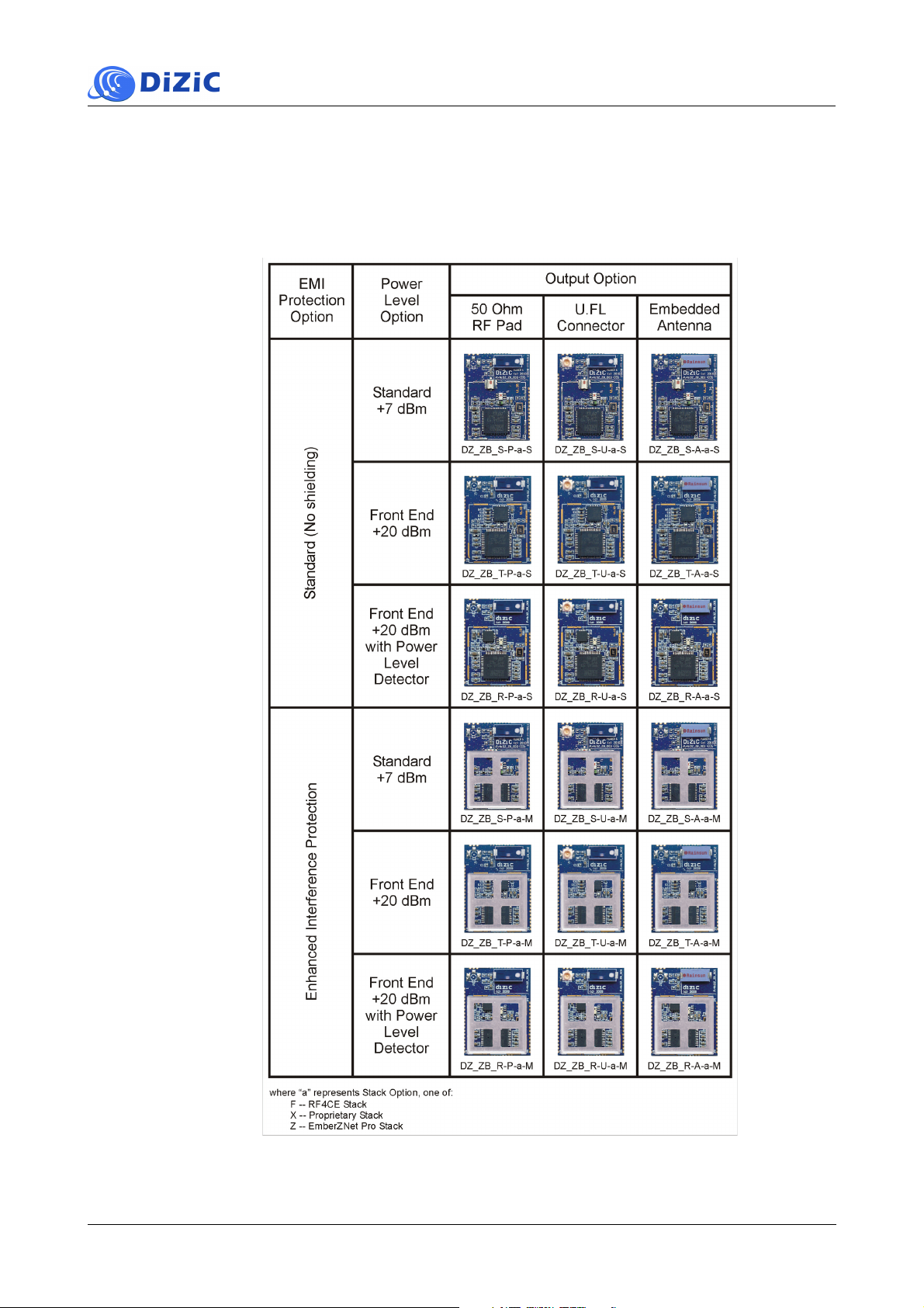
2 Configurations
Four set of options are used to configure the DZ-ZB Modules based on user requirements: Output
Options, Power Level Options, ZigBee Stack Options, and EMI Protection Options (not shown
below).
2 Configurations
DiZiC 802.15.4 DZ-ZB RF Modules
Figure 1: DZ-ZB module configurations
July 2010 Doc ID: PB-ZB-MOD-003-20DS Page 3
© 2010 DiZiC Co. Ltd. Subject to change without notice.
2 Configurations
DiZiC 802.15.4 DZ-ZB RF Modules
2.1 Power Level Options: Codes [S] [R] or [T]
Three power level options are available, including a standard module without a power amplifier
and two modules with power amplifiers sourced from two vendors.
Table 1: Power level options
Selector Option Description
[S] Standard + 7dBm STM32W chip: System on Chip - where radio, microcon-
troller, program/user memory, RAM, ZigBee protocols
stack are integrated in one chip.
[R] Front End (PA and LNA) with RF
output power level detector + 20
dBm
[T] Front End (PA and LNA) + 20 dBm ADD DESCRIPTION
ADD DESCRIPTION
2.2 RF Output Options: Codes [A] [P] or [U]
Three RF output options are available, including an onboard antenna, an RF pad, and an U.FL
connector.
Table 2: Output Options
Selector Option Description
[A] Embedded SMD Antenna ADD DESCRIPTION
[P] Single ended 50 Ω RF Pad ADD DESCRIPTION
[U] U.FL 50 Ω coaxial connector ADD DESCRIPTION
2.3 ZigBee Stack Options: Codes [F] [X] or [Z]
Three ZigBee stack options are available, including an RF4CE stack, a stack from Ember, and a
proprietary stack. Programming instructions for each of the ZigBee stacks are included on the
product CD.
Table 3: ZigBee Stack Options
Selector Option Description
[F] RF4CE stack ADD DESCRIPTION
[X] Proprietary stack ADD DESCRIPTION
[Z] EmberZnet PRO stack ADD DESCRIPTION
July 2010 Doc ID: PB-ZB-MOD-003-20DS Page 4
© 2010 DiZiC Co. Ltd. Subject to change without notice.
2.4 EMI Protection Options: [M] or [S]
A metal shield cap can be added to the module for EMI protection.
Table 4: SEMI Protection Options
Selector Option Description
[M] Metal shield cap Enables enhanced level of electromagnetic immunity (EMI)
protection.
[S] Standard module RF Module without metal shielding.
2.5 Configuration Options Matrix
Table 5 below shows all the available options for the DZ-ZB Module.
Table 5: DZ-ZB module options set
RF Output Output Power Level Software Stack EMI Protection
2 Configurations
DiZiC 802.15.4 DZ-ZB RF Modules
Cod
e
Description
A Embedded SMD
Cod
e
Description
Cod
e
Description
Cod
e
Description
S Standard + 7dBm F RF4CE stack M Metal shield cap
Antenna
P Single ended 50 Ω
RF Pad
R Front End (PA and
LNA) with RF out-
X Proprietary stack S Standard module
put power level
detector + 20 dBm
U U.FL 50 Ω coaxial
connector
T Front End (PA and
LNA) + 20 dBm
Z EmberZnet PRO
stack
With these options, a total of 54 configurations of the DZ-ZB module are possible. Table 6 provides
a matrix of these configurations and the associated codes, which are used when ordering the module.
A P U
F X Z F X Z F X Z
M S M S M S M S M S M S M S M S M S
Table 6: Configuration options matrix
S
R
T
July 2010 Doc ID: PB-ZB-MOD-003-20DS Page 5
ASFS
ASFM
ARFS
ARFM
ATFS
ATFM
ASXS
ASXM
ARXS
ARXM
ATZM
ATXM
© 2010 DiZiC Co. Ltd. Subject to change without notice.
AFZS
AFZM
ARZS
ARZM
ATZS
ATXS
PSFS
PSFM
PRFS
PRFM
AOFS
AOFM
PSXS
PSXM
PRXS
PRXM
AOXS
AOXM
PSZS
PSZM
PRXS
PRZM
AOZS
AOZM
USFS
USFM
URFS
URFM
UTFS
UTFM
USXS
USXM
URXS
URXM
UTXS
UTXM
USZS
USZM
URZS
URZM
UTZS
UTZM

2 Configurations
DiZiC 802.15.4 DZ-ZB RF Modules
July 2010 Doc ID: PB-ZB-MOD-003-20DS Page 6
© 2010 DiZiC Co. Ltd. Subject to change without notice.
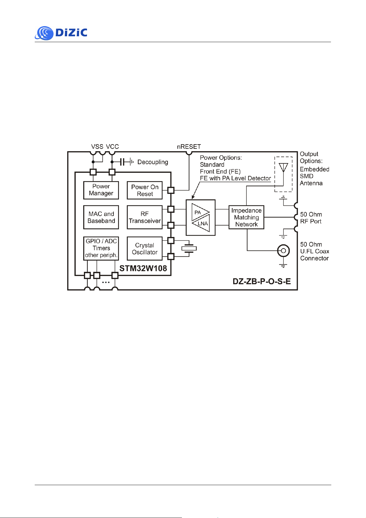
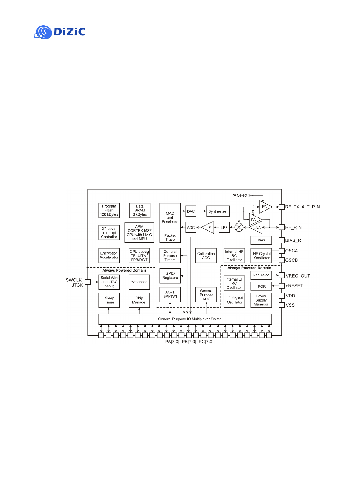
3 Block Diagram
The DZ-ZB Module is low-power, highly sensitivity IEEE 802.15.4 / ZigBee-compliant module. This
multi-functional device is based on the STMicroelectronics STM32W108 fully integrated Systemon-Chip
This STM32W108 SoC integrates a 2.4 GHz IEEE 802.15.4-compliant transceiver, a 32-bit ARM®
Cortex™- M3 microprocessor, Flash and RAM memory, as well as peripherals for use by designers of ZigBee-based systems
Figure 2 below shows a block diagram of the DZ-ZB Module.
[1]
(STM32W108CBU6x version).
3 Block Diagram
DiZiC 802.15.4 DZ-ZB RF Modules
[2]
.
Figure 2: Block diagram of DZ-ZB RF Modules
July 2010 Doc ID: PB-ZB-MOD-003-20DS Page 7
© 2010 DiZiC Co. Ltd. Subject to change without notice.
4 Absolute Maximum Ratings
DiZiC 802.15.4 DZ-ZB RF Modules
4 Absolute Maximum Ratings
Stresses above the absolute maximum ratings listed in this section may cause permanent damage
to the device. These are stress ratings only and functional operation of the device at these conditions is not implied. Exposure to maximum rating conditions for extended periods may affect
device reliability.
4.1 Voltage Characteristics
Table 7: Voltage characteristics
Ratings Min. Max. Unit
Regulator input voltage (VDD_PADS) -0.3 +3.6 V
RF Input Power (for max level for correct packet reception Receive characteristics) RX signal into a lossless
balun
Voltage on any GPIO (PA[7:0], PB[7:0], PC[7:0]), SWCLK, nRESET, VREG_OUT
4.2 Current Characteristics
Symbol Ratings Max. Unit
IVDD Total current into VDD/VDDA power lines (source) 150 mA
IVSS Total current out of VSS ground lines (sink) 150 mA
IIO Output current sunk by any I/O and control pin 25 mA
4.3 Thermal Characteristics
15 dBm
-0.3 VDD_PADS +0.3 V
Table 8: Current characteristics
Table 9: Thermal characteristics
Symbol Ratings Value Unit
TSTG Storage temperature range –40 to +140 °C
TJ Maximum junction temperature 150 °C
July 2010 Doc ID: PB-ZB-MOD-003-20DS Page 8
© 2010 DiZiC Co. Ltd. Subject to change without notice.
5 Components
This section describes the key components of the DZ-ZB Modules including the STM32W108
SoC, the RF Front End with RF Output Power Level Detector, the RF Front End (FE), and the ZigBee stacks.
5.1 STM32W108 – System-on-Chip Transceiver
The STM32W108 is a fully integrated System-on-Chip that includes:
+
2.4 GHz, IEEE 802.15.4 compliant transceiver
+
32-bit ARM® Cortex™ -M3 microprocessor
+
Flash and RAM memory
+
Peripherals for use of designers of ZigBee-based systems.
Figure 3 below shows the block diagram of STM32W108.
5 Components
DiZiC 802.15.4 DZ-ZB RF Modules
Figure 3: Block diagram of System-on-Chip STM32W108
5.2.1 IEEE 802.15.4 Compliant Transceiver
This SoC transceiver utilizes an efficient architecture that exceeds the dynamic range requirements imposed by the IEEE 802.15.4-2003 standard by over 15 dB. The integrated receive channel filtering allows for robust
co-existence with other communication standards in the 2.4 GHz spectrum such as IEEE 802.11
and Bluetooth. The integrated regulator, VCO, loop filter, and power amplifier keep the external
component count low. An optional high performance radio mode (boost mode) is software-selectable to boost dynamic range.
July 2010 Doc ID: PB-ZB-MOD-003-20DS Page 9
© 2010 DiZiC Co. Ltd. Subject to change without notice.

5 Components
DiZiC 802.15.4 DZ-ZB RF Modules
5.3.2 Operation Modes
The integrated 32-bit ARM® Cortex™-M3 microprocessor is highly optimized for high performance, low power consumption, and efficient memory utilization. With its integrated MPU, the
STM32W108 supports two different modes of operation: System mode and Application mode.
The networking stack software runs in System Mode with full access to all areas of the chip. Application code, however, runs in Application Mode with limited access to STM32W108 resources.
This allows for the scheduling of events by the application developer while preventing modification
of restricted areas of memory and registers. This architecture results in increased stability and reliability of deployed solutions.
5.4.3 Flash and RAM Memory
The STM32W108 has 128 Kbytes of embedded Flash memory and 8 Kbytes of integrated RAM for
data and program storage. The STM32W108 HAL software employs an effective wear-levelling
algorithm that optimizes the lifetime of the embedded Flash.
5.5.4 Integrated MAC Functions
To maintain the strict timing requirements imposed by ZigBee and IEEE 802.15.4-2003 standards,
the STM32W108 IC integrates a number of MAC functions into the hardware. The MAC hardware
handles automatic ACK transmission and reception, automatic back off delay, and clear channel
assessment for transmission, as well as automatic filtering of received packets. A packet trace
interface is also integrated in the MAC hardware allowing complete, non-intrusive capture of all
packets to and from the STM32W108 IC.
5.6.5 Power Management
The STM32W108 IC offers a number of advanced power management features that enables long
battery life. A high-frequency internal RC oscillator allows the processor core to begin code execution quickly upon waking. Various deep sleep modes are available with less than 1 µs power consumption while retaining RAM contents.
5.7.6 Peripherals
To support user-defined applications, on-chip peripherals include UART, SPI, TWI, ADC, generalpurpose timers, and up to 24 GPIOs. Additionally, an integrated voltage regulator, power-on-reset
circuit, and sleep timer are available.
5.8.7 Interfaces
The STM32W108 IC utilizes standard Serial Wire and JTAG interfaces for powerful software
debugging and programming of the ARM Cortex-M3 core. The STM32W108 IC integrates the
standard ARM system debug components including Flash Patch and Breakpoint (FPB), Data
Watch-point and Trace (DWT), and Instrumentation Trace Macrocell (ITM).
July 2010 Doc ID: PB-ZB-MOD-003-20DS Page 10
© 2010 DiZiC Co. Ltd. Subject to change without notice.
 Loading...