

DIZIC DZZBG User Manual
DZ-ZB-G IEEE 802.15.4/ZigBee RF Module
Quickly add wireless communication with these high performances modules
The DiZiC DZ-ZB-G 802.15.4 module series allows
you to quickly add wireless networking capabilities to
your products. These ZigBee-compliant modules are
ready-to-use, simple to operate, and available in a
wide range of configurations. They are ideal for
industrial sensors, consumer remote controls, home
appliances, and more.
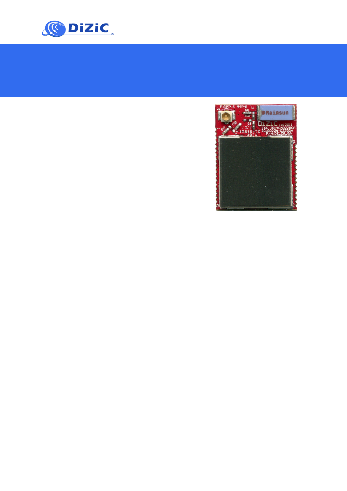
Compact Form Factor – With 25 mm by 19 mm, this
module can be shielded for enhanced EMI protection.
DZ-ZB-G Module with Shield
Complete System-on-Module
• 2.4 GHz CSS transceiver
• 32-bit ARM® Cortex-M3 processor
• 128 kB flash, 8kB RAM memory
• AES128 encryption accelerator
• Flexible ADC, UART serial communication, and
general purpose timers
• Highly configurable GPIO with Schmitt trigger inputs
Industry-leading ARM Cortex-M3 processor
• Leading 32-bit processing performance
• Highly efficient Thumb-2 instruction set
• Operation at 6, 12 or 24 MHz
• Flexible Nested Vectored Interrupt Controller
Innovative network and processor
debug
• Serial Wire Debug interface
• Standard ARM debug capabilities:
Flash Patch &Breakpoint; Data Watch-point & Trace
RF Performances
• Rx sensitivity (- 105 dBm)
• Tx output power level (+20 dBm)
Low power consumption, advanced
management
• RX Current (w/ CPU): 35 mA
• TX Current (w/ CPU, +20dBm) 130 mA
• Low deep sleep current, less than 6 μA
• Low-frequency internal RC oscillator for lowpower sleep timing
• High-frequency internal RC oscillator for fast
(100 usec) processor start-up from sleep
Target Applications
• Smart Energy
• Building automation and control (HVAC)
• Home automation and control
• Security and monitoring
• AMR/AMI
• Medical
• General ZigBee wireless sensor
networking
• Wireless hand-held terminals
• Industry telemetry /automatic data
collection
• Temperature and humidity control systems

Table of Content
1. Product Approvals.......................................................................................................................................4
1.1. FCC Approvals .....................................................................................................................................4
1.2. IC (Industry Canada) Approvals...........................................................................................................4
1.3. Product Warranty..................................................................................................................................5
2. Configuration...............................................................................................................................................6
2.1. Power Level Option [G]........................................................................................................................6
2.2. RF Output Options: Codes [A], [U], [X] or [E]....................................................................................6
2.3. Protocol Stack Options: Codes [F], [X] or [Z]......................................................................................6
2.4. EMI Protection Options: Codes [M] or [ ]....................................................................................... .....6
3. Block Diagram.............................................................................................................................................7
4. Absolute Maximum Rating..........................................................................................................................8
4.1. Voltage Characteristics .........................................................................................................................8
4.2. Current Characteristics..........................................................................................................................8
4.3. Thermal Characteristics ........................................................................................................................8
5. Components.................................................................................................................................................9
5.1. STM32W108 –System-on-Chip Transceiver........................................................................................9
5.1.1. IEEE802.15.4 Compliant Transceiver...................................................................................................9
5.1.2. Operation Modes...................................................................................................................................9
5.1.3. Flash and RAM Memory ....................................................................................................................10
5.1.4. Integrated MAC Functions..................................................................................................................10
5.1.5. Power Management.............................................................................................................................10
5.1.6. Peripherals...........................................................................................................................................10
5.1.7. Interfaces.............................................................................................................................................10
5.2. Protocol Stacks....................................................................................................................................11
6. Electrical Characteristics ...........................................................................................................................12
6.1. Parameter conditions ...........................................................................................................................12
6.1.1. Minimum and Maximum Values........................................................................................................12
6.1.2. Typical values.....................................................................................................................................12
6.2. Operating Conditions..........................................................................................................................12
6.2.1. General Operating Conditions.............................................................................................................12
6.2.2. Electrostatic Discharge (ESD) ............................................................................................................13
6.2.3. DC Characteristics ..............................................................................................................................13
6.3. RF Characteristic.................................................................................................................................15
6.3.1. Receiver Characteristics......................................................................................................................15
6.3.2. Transmitter Characteristics........................................................................................................................15
7. Mechanical Characteristics........................................................................................................................16
7.1. Module Pad Diagram..........................................................................................................................16
7.2. Module Pads........................................................................................................................................16
7.3. Module Mechanical Dimensions.........................................................................................................22
8. Soldering....................................................................................................................................................23
8.1. Soldering (Reflow) Profile..................................................................................................................23
8.2. Profile Parameters...............................................................................................................................23
8.3. Recommended Footprint.....................................................................................................................24
9. References .................................................................................................................................................25
Document Information ..........................................................................................................................................26
Revision History....................................................................................................................................................26
About DiZiC..........................................................................................................................................................26
October 2012 Doc ID:DZ DS-ZBGx MOD rev1.5
© 2012 DiZiC Co. Ltd. Subject to change without notice.
2

Table of Figures
Fig. 1 Simplified Block Diagram of the Module.....................................................................................................7
Fig. 2 Block diagram of System-on-Chip STM32W108.........................................................................................9
Fig. 3 Available protocol stacks. ...........................................................................................................................11
Fig. 4 Pad connection diagram for modules (top view).........................................................................................16
Fig. 5 Standard module dimensions without metal shielding................................................................................22
Fig. 6 Standard module dimensions with metal shielding.....................................................................................22
Fig. 7 Recommended Temperature Profile for Soldering (Reflow)......................................................................23
Fig. 8 Recommended Footprint for Module..........................................................................................................24
List of Tables
Table 1: Power level option.....................................................................................................................................6
Table 2: Output options...........................................................................................................................................6
Table 3: Protocol stack options................................................................................................................................6
Table 4: EMI protection options..............................................................................................................................6
Table 5: Functional description on Front End Module signals................................................................................7
Table 6: Voltage characteristics...............................................................................................................................8
Table 7: Current characteristics...............................................................................................................................8
Table 8: Thermal characteristics..............................................................................................................................8
Table 9: General operating conditions...................................................................................................................12
Table 10: ESD absolute maximum........................................................................................................................13
Table 11: DC electrical characteristics..................................................................................................................14
Table 12: Receiver characteristics.........................................................................................................................15
Table 13: Transmitter characteristics.....................................................................................................................15
Table 14: Pad description. .....................................................................................................................................21
Table 15: Solder Reflow Parameters.....................................................................................................................23
October 2012 Doc ID:DZ DS-ZBGx MOD rev1.5
© 2012 DiZiC Co. Ltd. Subject to change without notice.
3

1. Product Approvals
The DZ-ZB-G has been designed to meet all national regulations for world-wide use.
The transmitter module may not be co-located with any other transmitter or antenna.
Please be advised that DiZiC Co., Ltd. declares that the DZ-ZB-G module will be used exclusively by
OEM’s or ODM’s and will therefore not be directly accessible by end users.
The radio must be installed in a host that will have at least 20cm distance between radio’s antenna
and human body.
1.1. FCC Approvals
The DZ-ZB-G with PCB Antenna has been tested to comply with FCC CFR Part 15 (USA) The
devices meet the requirements for modular transmitter approval as detailed in the FCC public notice
DA00.1407.transmitter.
FCC statement:
This device complies with Part 15 of the FCC rules. Operation is subject to the following two
conditions: (1) this device may not cause harmful interference, and (2) this device must accept any
interference received, including interference that may cause undesired operation.
FCC ID: YCMDZZBG
The FCC requires the user to be notified that any changes or modifications made to this device that
are not expressly approved by the manufacturer may void the user's authority to operate the
equipment.
FCC Labeling Requirements
When integrating the DZ-ZB-G into a product it must be ensured that the FCC labeling requirements
are met. This includes a clearly visible label on the outside of the finished product specifying the DiZiC
FCC identifier (FCC ID: YCMDZZBG) as well as the FCC notice shown on the previous page. This
exterior label can use wording such as "Contains Transmitter Module FCC ID: YCMDZZBG “ or
"Contains FCC ID: YCMDZZBG " although any similar wording that expresses the same meaning may
be used.
1.2. IC (Industry Canada) Approvals
The DZ-ZB-SP with integrated Antenna has been tested to comply with IC.
IC-ID: 9022A- DZZBG
The labeling requirements for Industry Canada are similar to those of the FCC. Again, a clearly visibly
label must be placed on the outside of the finished product stating something like "Contains
Transmitter Module, IC: 9022A- DZZBG ", although any similar wording that expresses the same
meaning may be used.
IC (Industry Canada) statement:
This module complies with Industry Canada RF radiation exposure limits set forth for general
population/uncontrolled environment. This device complies with Industry Canada licence-exempt RSS
standard(s). Operation is subject to the following two conditions: (1) this device may not cause
interference, and (2) this device must accept any interference, including interference that may cause
undesired operation of the device.
The integrator is responsible for the final product to comply to IC ICES-003 and FCC Part 15, Sub. B Unintentional Radiators.
October 2012 Doc ID:DZ DS-ZBGx MOD rev1.5
© 2012 DiZiC Co. Ltd. Subject to change without notice.
4

Notice for channel 25:
Special care needs to be taken on channel 25 in order to not generate out of band signals.
At maximum duty cycle (100%) the setting shall be 7.56dBm (power setting -11) to pass the FCC
certification, however in more common cases where the duty cycle is lower than 100% the power
level can be increased according to FCC rules.
A simple method can be used to determine the maximum output level to be applied.
Duty cycle correction factor (dB) = 20 log (duty cycle)
Use of External Antenna:
The module has been approved with an external quarter wave dipole antenna of 2dBi gain.
Any use of an antenna with a gain > 2 dBi is strictly forbidden, unless the output power is reduced
accordingly.
1.3. Product Warranty
DiZiC warrants this product against defects in materials and workmanship for a period of 1 year. If a
defect is discovered, DiZiC will at its option, repair or replace the product at no charge provided it is
returned during the warranty period, with transportation charges prepaid, to the authorized DiZiC
dealer from whom you purchased the product. Proof of purchase may be required.
This warranty does not apply if the product has been damaged by accident, abuse, misuse, or
misapplication; if the product has been modified without the written permission of DiZiC; or if any
DiZiC serial number has been removed or defaced.
THE WARRANTY AND REMEDIES SET FORTH ABOVE ARE EXCLUSIVE IN LIEU OF ALL
OTHERS, WHETHER ORAL OR WRITTEN, EXPRESSED OR IMPLIED. DiZiC SPECIFICALLY
DISCLAIMS ANY AND ALL IMPLIED WARRANTIES, INCLUDING, WITHOUT LIMITATION,
WARRANTIES OF MERCHANTABILITY AND FITNESS FOR A PARTICULAR PURPOSE.
No DiZiC dealer, agent, or employee is authorized to make any modification, extension, or addition to
this warranty.
DiZiC IS NOT RESPONSIBLE FOR SPECIAL, INCIDENTAL, OR CONSEQUENTIAL DAMAGES
RESULTING FROM ANY BREACH OF WARRANTY, OR UNDER ANY OTHER LEGAL THEORY,
INCLUDING BUT NOT LIMITED TO LOST PROFITS, DOWNTIME, GOODWILL, DAMAGE TO OR
REPROGRAMMING, OR REPRODUCING ANY PROGRAM OR DATA STORED IN OR USED WITH
DiZiC PRODUCTS.
Some states do not allow the exclusion or limitation of incidental or consequential damages or
exclusions of implied warranties, so the above limitations of exclusions may not apply to you. This
warranty gives you specific legal rights, and you may also have other rights that vary from state to
state.
October 2012 Doc ID:DZ DS-ZBGx MOD rev1.5
© 2012 DiZiC Co. Ltd. Subject to change without notice.
5
2. Configuration
The module comes with different configuration options. RF Output Options, Protocol Stack Options,
and EMI Protection Options.
2.1. Power Level Option [G]
The module DZ-ZB has the power option G preselected.
Selector Options Description
STM32W chip: System on Chip - where radio, microcon-
[G] Standard + 20dBm
Table 1: Power level option
2.2. RF Output Options: Codes [A], [U], [X] or [E]
Three RF output options are available, including an onboard antenna and an U.FL connector.
troller, program/user memory, RAM, ZigBee protocols
stack are integrated in one chi
Selector Options Description
[A] Embedded SMD Antenna
[U]
[X]
[E]
Table 2: Output options
U.FL 50 coaxial connector
Embedded SMD Antenna and
U.FL 50 coaxial connector
With +2dBi external Dipole
antenna
2.3. Protocol Stack Options: Codes [F], [X] or [Z]
Three protocol stack options are available, including an RF4CE stack, a Zigbee Pro stack from Ember,
and a proprietary MAC/Phy stack
Selector Options Description
[F] RF4CE stack
[X] Proprietary stack
[Z] EmberZnet PRO stack
Table 3: Protocol stack options
2.4. EMI Protection Options: Codes [M] or [ ]
A metal shield cap can be added to the module for EMI protection.
Selector Options Description
[M] Metal shield cap
Enables enhanced level of electromagnetic immunity
(EMI) protection.
[ ] Standard module RF Module without metal shielding
Table 4: EMI protection options
October 2012 Doc ID:DZ DS-ZBGx MOD rev1.5
© 2012 DiZiC Co. Ltd. Subject to change without notice.
6
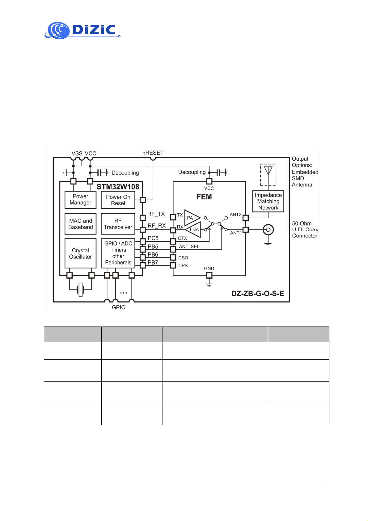
3. Block Diagram
The DZ-ZB Module is low-power, highly sensitivity IEEE 802.15.4 / ZigBee-compliant module. This
multi-functional device is based on the STMicroelectronics STM32W108 fully integrated System-onChip [1] (STM32W108CBU6x version).
This STM32W108 SoC integrates a 2.4 GHz IEEE 802.15.4-compliant transceiver, a 32-bit ARM®
Cortex™- M3 microprocessor, Flash and RAM memory, as well as peripherals for use by designers of
ZigBee-based systems [2]
Fig. 1 Simplified Block Diagram of the Module
FEM Signal name Direction Description
TxRx Digital input to FEM
ANT_SEL Digital input to FEM
CSD Digital input to FEM
CPS Digital input to FEM
Table 5: Functional description on Front End Module signals.
TxRx = 1: Transmit Mode
TxRx = 0: Receive Mode
Antenna Switch:
ANT_SEL = 0: Select UF.L connector.
ANT_SEL = 1: Select SMD antenna.
Sleep mode
CPS = 0: All OFF low power mode
CPS = 1: Power ON
LNA Control
CPS = 0: LNA OFF bypass mode
CPS = 1: LNA ON
October 2012 Doc ID:DZ DS-ZBGx MOD rev1.5
© 2012 DiZiC Co. Ltd. Subject to change without notice.
STM32W108
Port name
PC5, TX_ACTIVE
PB5
PB6
PB7
7
4. Absolute Maximum Rating
Stresses above the absolute maximum ratings listed in this section may cause permanent damage to
the device. These are stress ratings only and functional operation of the device at these conditions is
not implied. Exposure to maximum rating conditions for extended periods may affect device reliability
4.1. Voltage Characteristics
Ratings Min. Max. Unit
VCC input voltage (VDD_PADS) -0.3 +3.6 V
RF Input Power (for max level for correct packet reception
Receive characteristics) RX signal input
Voltage on any GPIO (PA[7:0], PB[7:0], PC[7:0]), SWCLK,
nRESET
Table 6: Voltage characteristics
15 dBm
-0.3
VDD_PADS
+0.3
V
4.2. Current Characteristics
Symbol Ratings Max. Unit
IVDD Total current into VDD/VDDA power lines (source) 150 mA
IVSS Total current out of VSS ground lines (sink) 150 mA
IIO Output current sunk by any I/O and control pin 25 mA
Table 7: Current characteristics
4.3. Thermal Characteristics
Symbol Ratings Value Unit
TSTG Storage temperature range -40 to +85 °C
TJ Maximum junction temperature 150 °C
Table 8: Thermal characteristics
October 2012 Doc ID:DZ DS-ZBGx MOD rev1.5
© 2012 DiZiC Co. Ltd. Subject to change without notice.
8
 Loading...