

Page 1
查询DEM16216SYH-PY供应商查询DEM16216SYH-PY供应商
Display Elektronik GmbH
LCD MODULE
DEM 16216 SYH-PY
Product specification Version: 4
09.04.2003
Page 2
GENERAL SPECIFICATION
DEM 16216 SYH-PY
CUSTOMER P / N
VERSION NO. CHANGE DESCRIPTION DATE
MODULE N0. :
0
1
2
3
4
PREPARED BY: ZXD DATE:
CHANGE LCD AND BACKLIGHT 2001/01/31
ORIGINAL VERSION 2001/01/16
ADD VERSION 2002/10/14
ADD MODEL 2002/11/15
2001/01/18CHANGE AS KS0070B
15.11.2002
APPROVED BY: MH DATE:
09.04.2003
Page 3

DEM 16216 SYH-PY Product specification
1. FUNCTIONS & FEATURES -------------------------------------------------------------------
2. MECHANICAL SPECIFICATIONS -------------------------------------------------------------------------------------------
3. BLOCK DIAGRAM -------------------------------------------------------------------------------
4. EXTERNAL DIMENSIONS --------------------------------------------------------------------
5. PIN ASSIGNMENT -----------------------------------------------------------------------------
6.1 PCB DRAWING AND DESCRIPTION------------------------------------------------------
6.2 EXAMPLE APPLICATION -------------------------------------------------------------------------
6.3 THE MODULE NO. IS PRINTED ON THE PCB -------------------------------------------------------------------------
7. BACKLIGHT VOLTAGE & CURRENT--------------------------------------------------------------------------
8. DISPLAY DATA RAM (DDRAM) ---------------------------------------------------------------------------
9. INSTRUCTION DESCRIPTION---------------------------------------------------------------
10. INTERFACE WITH MPU IN BUS MODE---------------------------------------------------------
1). Interface with 8-bit MPU ----------------------------------------------------------------------------------------------------------------
2). Interface with 4-bit MPU ----------------------------------------------------------------------------------------------------------------
11. INITIALIZING BY INSTRUCTION ---------------------------------------------------------------------------
1). 8-bit interface mode ----------------------------------------------------------------------------------------------------------------
2). 4-bit interface mode ----------------------------------------------------------------------------------------------------------------
12. MAXIMUM ABSOLUTE POWER RATINGS-----------------------------------------------------------
13. ELECTRICAL CHARACTERISTICS --------------------------------------------------------
----------------------------------------------------------------------------------------------
------------------------------------------------------------------------------------------------
---------------------------------------------------------------------------------------------------------
-----------------------------------------------------------------------------------------------------------
14. STANDARD CHARACTER PATTERN ---------------------------------------------------------------------------
15. FRAME FREQUENCY--------------------------------------------------------------------------
16. LCD MODULES HANDLING PRECAUTIONS-----------------------------------------------
17. OTHERS ---------------------------------------------------------------------------------------------------
CONTENTS
2
2
2
3
3
4
5
5
6
6
13-1 DC CHARACTERISTICS
13-2-1 AC CHARACTERISTICS
13-2-2 WRITE MODE
13-2-3 READ MODE
7
11
11
11
12
12
13
14
14
14
16
17
17
18
19
20
21
VERSION : 4 1
Page 4
DEM 16216 SYH-PY Product specification
E
LCD
R/W
controller
RS
LSI
V
0
V
Figure 1.0
BACKLIGHT
1. FUNCTIONS & FEATURES
DEM 16216-SERIES type:
MODULE
DEM 16216 SYH-PY
Viewing Direction : 6 O'clock
Driving Scheme : 1/16 Duty Cycle, 1/5 Bias
Power Supply Voltage : 2.7V to 5.5V (typ. 5V)
Display Format : 16 x 2 Characters ( 5 x 8 dots, Format : 192 Kinds)
Internal Memory : CGROM ( 8,320 bits )
: CGRAM ( 64 x 8 bits )
: DDRAM ( 80 x 8 bits for Digits )
Interface : Easy Interface with a 4 - bit or 8 - bit MPU
VLCD Adjustable for Best Contrast
Backlight : Yellow/Green (lightpipe/lightguide)
LCD-TYPE
STN Yellow/Green
: 4.5V (typ.)
LCD TYPE
Transflective Positive Mode
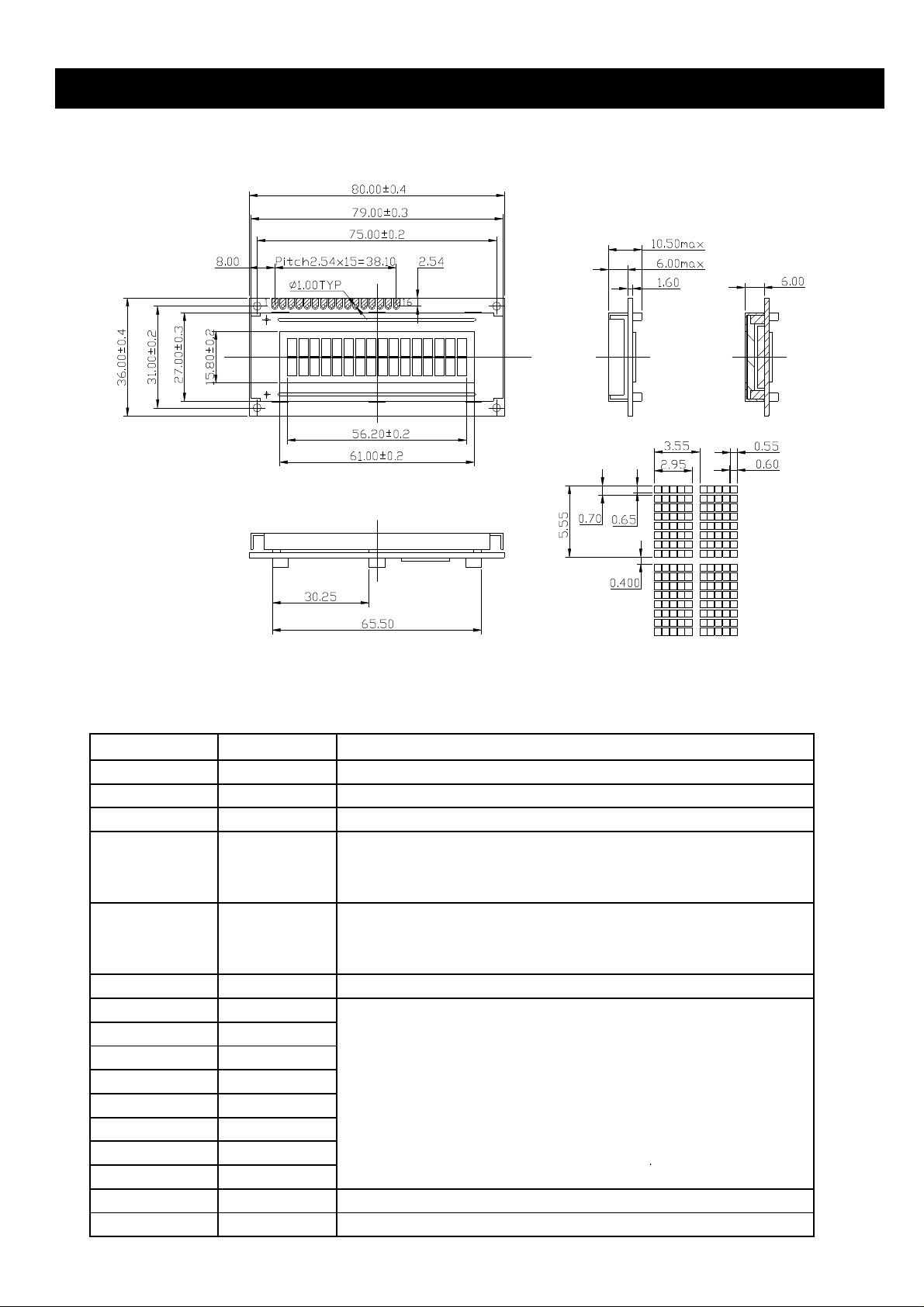
2. MECHANICAL SPECIFICATIONS
Character Pitch
Character Size : 2.95(w) x 5.55(h) mm
Character Font
Dot Size
Dot Pitch
: 3.55(w) x 5.95(h) mm
: 5 x 8 dots
: 0.55(w) x 0.65(h) mm
: 0.60(w) x 0.70(h) mm
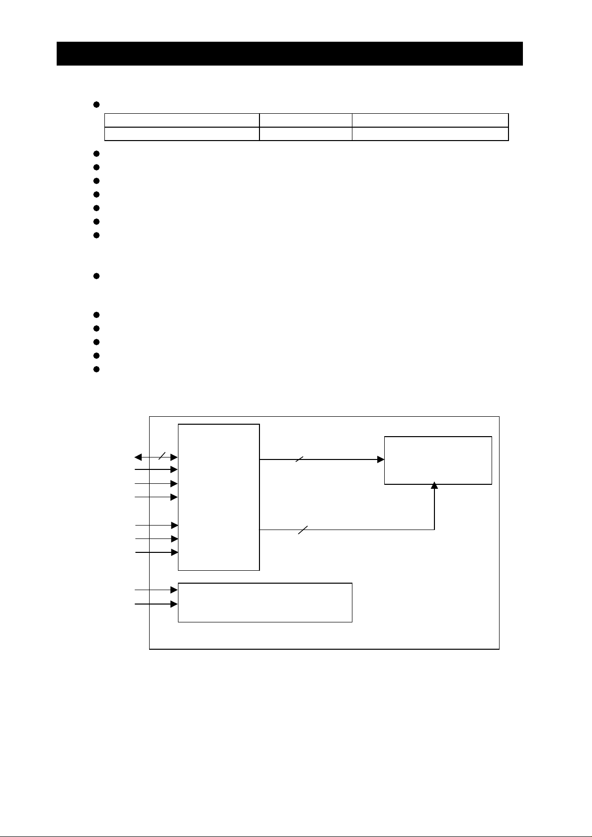
3. BLOCK Diagram
DB0~DB7
KS0070B-00
VDD
SS
A
K
COM1~COM16
SEG1~SEG80
LCD PANEL
2line*16characters
VERSION: 4 2
Page 5
DEM 16216 SYH-PY Product specification
4. External Dimensions
Figure 2.0
5. PIN Assignment
Pin No. Symbol Function
1 VSS Ground terminal of module
2 VDD Supply terminal of module 2.7 to 5.5 V
3 V0 Power Supply for Liquid crystal Drive
4 RS Register Select
RS = 0… Instruction Register
RS = 1… Data Register
5 R/W Read / Write
R/W = 1 (Read)
R/W = 0 (Write)
6 E Enable
7 DB0
8 DB1 Bi-directional Data Bus, Data Transfer is performed
9 DB2 once , thru DB0~DB7 , in the case of interface data .
10 DB3 Length is 8-bits; and twice , thru DB4~DB7 in the case
11 DB4 of interface data length is 4-bits .
12 DB5 Upper four bits first then lower four bits .
13 DB6
14 DB7
15 LED - ( K ) Please also refer to 6.1 PCB drawing and description .
16 LED + ( A ) Please also refer to 6.1 PCB drawing and description .
VERSION : 4 3
Page 6

DEM 16216 SYH-PY Product specification
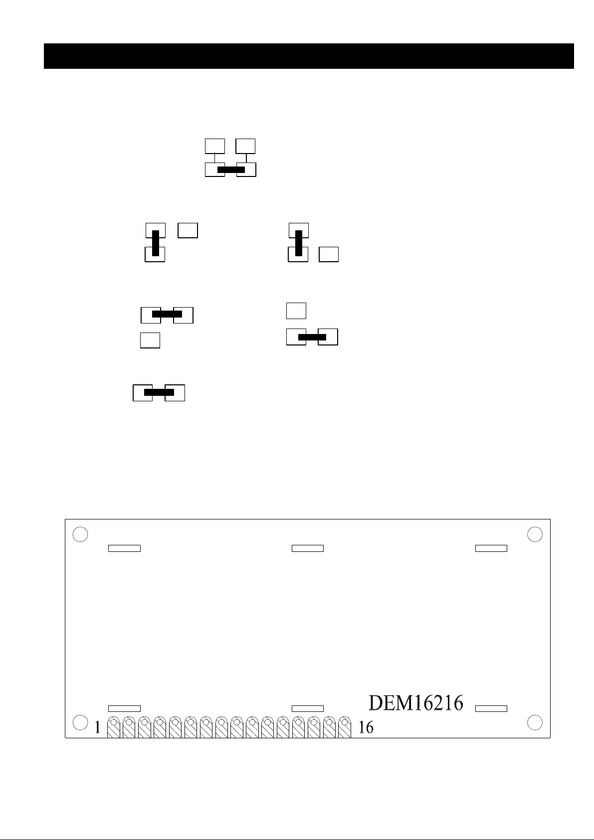
6.1 PCB DRAWING AND DESCRIPTION
Figure 3.0
Description :
6-1-1.The polarity of the pin 15 and the pin 16
Symbol J3,J5 J2,J4
Symbol State 15 Pin 16 Pin
J2,J4 Each Open Anode Cathode
J3,J5 Each Open Cathode Anode
6-1-2. The metal-bezel should be on gronud when the J1 is Solder- Bridge .
6-1-3. The LED Resistor should be bridged when the J6 is Solder-Bridge .
6-1-4. The R7 is the LED Resistor. (R7=24 Ohm)
Each Solder- Bridge
Each Solder- Bridge
LED Polarity
VERSION : 4 4
Page 7
DEM 16216 SYH-PY Product specification
J4
J2
6.2 Example application
6-2-1 The LED resistor should be bridged as following .
R7
J6
6-2-2 The 15 pin is the Anode and the 16 pin is the cathode as following .
J4 J2
6-2-3 The 15 pin is the cathode and the 16 pin is the Anode as following .
6-2-4 The metal-bezel is on ground as following .
J5
J3
J5
J3
J1
6.3 The module No. Is printed on the PCB .
Figure 4.0
VERSION : 4 5
Page 8

DEM 16102 SYH-PY Product specification
7. BACKLIGHT &SWITCH (Ta = -25 ~ +75°C)
Item
Backlight Voltage V
Backlight Current I
Symbol
Standard Value Unit
~33 mA
A
K
Figure 5.0
8. DISPLAY DATA RAM ( DDRAM )
1 2 3 4 5 6 7 8 9 10 11 12 13 14 15 16 DISPLAY POSITION
00 01 02 03 04 05 06 07 08 09 0A 0B 0C 0D 0E 0F DDRAM ADDRESS
40 41 42 43 44 45 46 47 48 49 4A 4B 4C 4D 4E 4F
Applicable Terminal
5
V
LED+ / LED-
A
K
VERSION: 4 6
Page 9

DEM 16216 SYH-PY Product specification
9. INSTRUCTION DESCRIPTION (IE = "LOW" )
1) Clear Display
2) Return Home
000000001
x
3) Entry Mode Set
00000001I/D
SH
9. INSTRUCTION DESCRIPTION
Outline
To overcome the speed difference between the internal clock of KS0070B and the MPU clock, KS0070B performs
internal operations by storing control information to IR or DR. The internal operation is determined according to the
signal from MPU, composed of read/write and data bus (Refer to Table 5 ).
Instruction can be divided largely into four kinds .
(1) KS0070B function set instructions ( set display methods, set data length, etc. )
(2) address set instruction to internal RAM
(3) data transfer instructions with internal ram
(4) others .
The address of the internal RAM is automatically increased or decreased by 1 .
*NOTE : During internal operation, Busy Flag (DB7) is read "1". Busy Flag check must be preceded by the
next instruction .
When you make an MPU program with checking the Busy Flag (DB7), it must be necessary
1/2 Fosc for executing the next instruction by falling E signal after the Busy Flag (DB7) goes to "0" .
Contents
RS R/W DB7 DB6 DB5 DB4 DB3 DB2 DB1 DB0
0 0 0 0 0 0 0 0 0 1
Clear all the display data by writing "20H" (space code) to all DRAM addresses, and set the DRAM addresses
to "00H" in the AC (address counter). Return cursor to original status, namely, bring the cursor to the left edge
on first line of the display . Make entry mode increment (I/D = "1" ) .
RS R/W DB7 DB6 DB5 DB4 DB3 DB2 DB1 DB0
Return Home is the cursor return home instruction .
Set DRAM address to "00H" in the address counter. Return cursor to its original site and return display to its
original status, if shifted, Contents of DDRAM does not change .
RS R/W DB7 DB6 DB5 DB4 DB3 DB2 DB1 DB0
Set the moving direction of cursor and display .
I/D : Increment/decrement of DDRAM address (cursor or blink )
When I/D = "1" , cursor/blink moves to right and DDRAM address is increased by 1.
When I/D = "0" , cursor/blink moves to left and DDRAM address is increased by 1.
*CGRAM operates the same as DDRAM , when reading from or writing to CGRAM .
SH: Shift of entire display
When DDRAM is in read (CGRAM read/write) operation or SH = "0" , shift of entire display is not performed .
If SH = "1" and in DDRAM write operation, shift of entire display is performed according to I/D value
(I/D = "1" : shift left, I/D = "0" : shift right ).
VERSION : 4
7
Page 10

DEM 16216 SYH-PY Product specification
9. INSTRUCTION DESCRIPTION (IE = "LOW" )
9. INSTRUCTION DESCRIPTION (IE = "LOW" )
Note that display shift is performed simultaneously in all the line .
0
0
0
1
1
0
1
1
9. INSTRUCTION DESCRIPTION (IE = "LOW" )
6).Function Set
4).Display ON/OFF CONTROL
RS R/W DB7 DB6 DB5 DB4 DB3 DB2 DB1 DB0
0 0 0 0 0 0 1 D C B
Control display/cursor/blink ON/OFF 1 bit register.
D : Display ON/OFF control bit
When D = "1" , entire display is turned on .
When D = "0" , display is turned off, but display data is remained in DDRAM .
C : Cursor ON/OFF control bit
When C = "1" , cursor is turned on.
When C = "0" , cursor is disappeared in current display, but I/D register remains its data .
B : Cursor Blink ON/OFF control bit
When B = "1" , cursor blink is on , that performs alternate between all the "1" data and display character at
the cursor position.
When B = "0" , blink is off.
5).Cursor or Display Shift
RS R/W DB7 DB6 DB5 DB4 DB3 DB2 DB1 DB0
0 0 0 0 0 1 S/C R/L X X
Without writing or reading of display data , Shift right/left cursor position or display
This instruction is used to correct or search display data . (Refer to Table 4)
During 2-line mode display, cursor moves to the 2nd line after 40th digit of 1st line .
When displayed data is shifted repeatedly, each line shifted individually .
When displayed shift is performed, the contents of address counter are not changed .
Table 4 Shift patterns according to S/C and R/L bits
S/C R/L Operation
Shift cursor to the left, AC is decreased by 1
Shift cursor to the right, AC is decreased by 2
Shift all the display to the left, cursor moves according to the display
Shift all the display to the right, cursor moves according to the display
RS R/W DB7 DB6 DB5 DB4 DB3 DB2 DB1 DB0
0 0 0 0 1 DL N F X X
DL : Interface data length control bit
When DL = "1" , it means 8-bit bus mode with MPU.
When DL = "0" , it means 4-bit bus mode with MPU. So to speak, DL is a signal to select 8-bit or 4-bit bus mode .
When 4-bit bus mode, it needs to transfer 4-bit data in two parts .
N : Display line number control bit
When N = "1" , 2-Line display mode is set .
When N = "0" , 1-Line display mode is set .
F : Display font type control bit
When F = "0" , 5 X 7 dots format display mode .
When F = "1" , 5 X 10 dots format display mode .
VERSION : 4 8
Page 11

DEM 16216 SYH-PY Product specification
9) Read Busy Flag & Address
00BF
AC6
AC5
AC4
AC3
AC2
AC1
AC0
10) Write data to RAM
10D7D6D5D4D3D2D1
D0
11) Read data from RAM
11D7D6D5D4D3D2D1
D0
7).Set CGRAM Address
RS R/W DB7 DB6 DB5 DB4 DB3 DB2 DB1 DB0
0 0 0 1 AC5 AC4 AC3 AC2 AC1 AC0
Set CGRAM Address to AC .
This instruction makes CGRAM data available from MPU.
8).Set DDRAM Address
RS R/W DB7 DB6 DB5 DB4 DB3 DB2 DB1 DB0
0 0 1 AC6 AC5 AC4 AC3 AC2 AC1 AC0
Set DDRAM Address to AC .
This instruction makes DDRAM data available from MPU.
In 1-line display mode (N=0, NW=0), DDRAM address is from "00H" to "4FH".
In 2-line display mode (N=1, NW=0), DDRAM address in the 1st line is from "00H" to "27H",and DDRAM address in
the 2nd line is from "40H" to "67H".
RS R/W DB7 DB6 DB5 DB4 DB3 DB2 DB1 DB0
This instruction shows whether KS0070B is in internal operation or not. If the resultant BF is High, the internal operaation is in progress and should wait until BF to become "Low", which by then the next instruction can be performed.
In this instruction value of address counter can also be read.
RS R/W DB7 DB6 DB5 DB4 DB3 DB2 DB1 DB0
Write binary 8-bit data to DRAM/CRAM/SEAGRAM.
The selection of RAM from DRAM, CRAM or SEAGRAM, is set by the previous address set instruction: DDRAM
address set, CGRAM address set, SEGRAM address set, RAM set instruction can also determines the AC
direction to RAM.
After write operation, the address is automatically increased/decreased by 1, according to the entry mode.
RS R/W DB7 DB6 DB5 DB4 DB3 DB2 DB1 DB0
Read binary 8-bit data to DDRAM/CRAM .
The selection of RAM is set by the previous address set instruction. If address set instruction of RAM is not
performed before this instruction, the data that read first is invalid, as the direction of AC is not determined. If the
RAM data is read several times without RAM address set instruction before read operation, the correct RAM data
from the second, but the first data would be incorrect, as there is not time to transfer RAM data. In case of DDRAM
read operation, cursor shift instruction plays the same role as DDRAM address set instruction: it also transfer RAM
data to output data register.
After read operation address counter is automatically increased/decreased by 1 according to the entry mode.
After CGRAM read operation, display shift may not be executed correctly.
*In case of RAM write operation, AC is increased/decreased by 1 like read operation after this. In this time, AC
indicates the next address position, but the previous data can only by read instruction.
VERSION : 4 9
Page 12

DEM 16216 SYH-PY Product specification
(CONTINUED)
Table 5. Instruction Set
Instruction code
Instruction RS R/WDB7 DB6 DB5 DB4 DB3 DB2 DB1 DB0 time (fosc
Execution
Description
=270KHz)
clear 0 0 0 0 0 0 0 0 0 1 1.53ms Write "20H" to DDRAM. And set
Display DDRAM address to "00H" from AC .
Set DDRAM address to "00H" from AC
Return 0 0 0 0 0 0 0 0 1 X 1.53ms and return cursor to its original position
home if shifted.
Entry 0 0 0 0 0 0 0 1 I/D SH 39us Assign cursor moving direction and
mode set enable the shift of entire display
Display on/ 0 0 0 0 0 0 1 D C B 39us Set display (D), cursor (C), and blinking
off control of cursor (B) on/off control bit .
Cursor or 0 0 0 0 0 1 S/C R/L X X 39us Set cursor moving and display shift
Display control bit , and the direction , without
shift changing of DRAM data .
Function Set interface data length (DL : 4-bit/8-bit),
Set 0 0 0 0 1 DL N F X X 39us numbers of display line (N : 1-line/2-line,
Display font type (F: 0…)
Set CGRAM 0 0 0 1 AC5 AC4 AC3 AC2 AC1 AC0 39us Set CGRAM address in address counter.
Address
Set DDRAM 0 0 1 AC6 AC5 AC4 AC3 AC2 AC1 AC0 39us Set DDRAM address in address counter.
Address
Read Busy Whether during internal operation or not
flag and 0 1 BF AC6 AC5 AC4 AC3 AC2 AC1 AC0 0us can be known by reading BF.
Address The contents of address counter can
also be read .
Write Data 1 0 D7 D6 D5 D4 D3 D2 D1 D0 43us Write data into internal RAM
to RAM ( DDRAM/CGRAM )
Read Data 1 1 D7 D6 D5 D4 D3 D2 D1 D0 43us Read data into internal RAM
from RAM ( DDRAM/CGRAM )
NOTE : When you make an MPU program with checking the Bus Flag (DB7), it must be necessary 1/2F osc for
executing the next instruction by falling E signal after the Busy Flag (DB7) goes to "0" .
VERSION : 4 10
Page 13
DEM 16216 SYH-PY Product specification
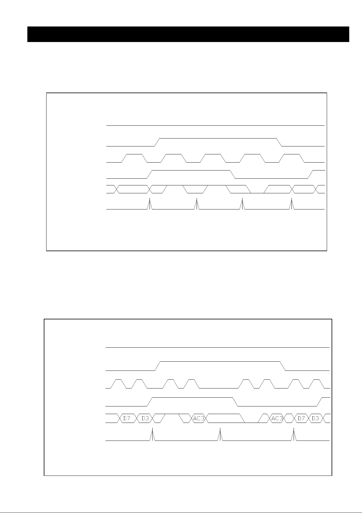
10. INTERFACE WITH MPU IN BUS MODE
1). Interface with 8-bit MPU
When interface data length are 8-bits , transfer is performed all at once through 8 ports. From DB0 to DB7 .
An Example of timing sequence is shown below .
RS
R/W
E
internal Singnal
DB7
Data
instruction
internal Operation
Busy Busy
Busy Flag
check
Busy Flag
check
No
Busy
Busy Flag
check
Data
instruction
Figure 6.0. Example of 8-bit bus mode timing Diagram
2) Interface with 4-bits MPU
When interfacing data length aref 4-bits , only 4 ports, from DB4 to DB7 , are used as data bus .
At first, higher 4-bit (in case of 8-bit bus mode, the contents of DB4~DB7) are transferred, and then the lower 4-bit
(in case of 8-bit bus mode, the contents of DB0~DB3) are transferred. So transfer is performed in two parts. Busy
Flag outputs"1" after the second transfer are ended.
Example of timing sequence is shown below .
RS
R/W
E
internal Singnal
DB7
instruction
VERSION : 4 11
Figure 7.0 Example of 4-bit bus mode timing Diagram
internal Operation
Busy
Busy Flag check
No
Busy
Busy Flag Check
instruction
Page 14

DEM 16216 SYH-PY Product specification
after V
rises to 4.5v
11. INITIALIZING BY INSTRUCTION
11-1 8-bit interface mode
Power on
Condition : fosc=270kHz
Wait for more than 30ms
DD
Function set 1 2-line mode
RS RW DB7 DB6 DB5 DB4 DB3 DB2 DB1 DB0
0 0 0 0 1 1 N F X X 0 5 x 7 dots
Wait for more than 39us
Display on/off control 1 display on
RS RW DB7 DB6 DB5 DB4 DB3 DB2 DB1 DB0
0 0 0 0 0 0 1 D C B 0 cursor off
Wait for more than 39us 0 blink off
Clear Display
RS RW DB7 DB6 DB5 DB4 DB3 DB2 DB1 DB0
0 0 0 0 0 0 0 0 0 1
N
F
D
C
B
0 1-line mode
1 5 x 10 dots
0 display off
1 cursor on
1 blink on
Wait for more than 1.53ms
I/D
Entry mode set
RS RW DB7 DB6 DB5 DB4 DB3 DB2 DB1 DB0
0 0 0 0 0 0 0 1 I/D SH 0 entire shift off
Initialization end
SH
0 decrement mode
1 increment mode
1 entire shift on
VERSION : 4 12
Page 15

DEM 16216 SYH-PY Product specification
after V
rises to 4.5v
11-2 4-bit interface mode
Power on
Condition : fosc=270kHz
Wait for more than 30ms
DD
Function set 1 2-line mode
RS RW DB7 DB6 DB5 DB4 DB3 DB2 DB1 DB0
0 0 0 0 1 0 X X X X 0 5 x 7 dots
0 0 0 0 1 0 X X X X 1 5 x 10 dots
0 0 N F X X X X X X
Wait for more than 39us
Display On/Off Control 1 display on
RS RW DB7 DB6 DB5 DB4 DB3 DB2 DB1 DB0
0 0 0 0 0 0 X X X X 0 cursor off
0 0 1 D C B X X X X 1 cursor on
Wait for more than 39us 1 blink on
Clear Display
RS RW DB7 DB6 DB5 DB4 DB3 DB2 DB1 DB0
0 0 0 0 0 0 X X X X
0 0 0 0 0 1 X X X X
N
F
D
C
B
0 1-line mode
0 display off
0 blink off
Wait for more than 1.53ms
Entry mode set 0 decrement mode
RS RW DB7 DB6 DB5 DB4 DB3 DB2 DB1 DB0 1 increment mode
0 0 0 0 0 0 X X X X
0 0 0 0 I/D SH X X X X
Initialization end
I/D
SH
0 entire shift off
1 entire shift on
VERSION : 4
13
Page 16

DEM 16216 SYH-PY Product specification
VDD4,5
5,5VI
0,7
1.0
I
0.4
0.6
external clock operation
Input Voltage(1)
V
2.2
VDD(except OSC1)
V
-0,3
0,6
Input Voltage(2)
V
VDD-1.0
VDD( OSC1)
V
-0.2
1.0
V
2,4
(DB0 TO DB7)
V
0,4
V
0.9V
(except
DB0 TO DB7
)
V
0.1V
Vd
1
Vd
1
Input Leakage Current
IIL-11VIN=0 V to V
Low Input Current
IIN-50
-125
-250
Internal Clock
f
190
270
350
fEC150
250
350
kHz
tR,tF0,2usLCD Driving Voltage
V
4.6
10.0
V
T
°C
12. MAXIMUM ABSOLUTE POWER RATINGS (Ta = 25°C)
Item Symbol Unit
Power supply voltage(1) -0.3 ~ +7.0
Power supply voltage(2)
Input voltage
Operating temperature -20 ~ +70
Storage temperature -30 ~ +80
13. Electrical Characteristics
13-1-1. DC Characteristics (V
Characteristic Symbol Unit
Operating Voltage
Supply Current Resistor oscillation mA
DD
DD1
DD2
Standard value
V
DD
V
0
V
IN
VDD-15.0 ~ VDD+0.3
-0.3 ~ VDD+0.3
Topr °C
stg
= 4.5V ~ 5.5V, Ta = -20 ~ +70°C)
Standard Value Test
MIN TYP MAX Condition
ceramic resonator
fosc = 250kHz
V
V
V
fosc = 270kHz
Output Voltage (1)
Output Voltage (2)
Voltage Drop
IH1
IL1
IH2
IL2
OH1
OL1
OH2
OL2
COM
SEG
DD
DD
IOH=-0.205mA
IOL=1.2uA
IOH=-40uA
IOL=40uA
IO = ±0.1mA
DD
V
V
V
V
V
uA
VIN=0V,VDD=5V(pull up)
OSC
(external Rf)
Rf = 91k ± 2%
(VDD=5V)
kHz
External Clock duty 45 50 55 %
VERSION : 4 14
LCD
VDD-V5 (1/5 Bias )
Page 17

DEM 16216 SYH-PY Product specification
VDD2.7
5,5VI
0.3
0.5
I
0.17
0.3
external clock operation
Input Voltage(1)
V
0.7V
VDD(except OSC1)
V
-0,3
0.4
Input Voltage(2)
V
0.7V
VDD( OSC1)
V
0.2V
V
2
(DB0 TO DB7)
V
0,4
V
0.8V
(except
DB0 TO DB7
)
V
0.2V
Vd
1
Vd
1,5
Input Leakage Current
IIL-11VIN=0 V to V
Low Input Current
IIN-10
-50
-120
Internal Clock
f
190
250
350
fEC125
270
350
kHz
tR,tF0,2usLCD Driving Voltage
V
3.0
10.0
V
( CONTINUED )
(V
= 2.7V ~ 5.5V; Ta = -20 ~ +70°C)
DD
Characteristic Symbol Unit
Standard Value Test
MIN TYP MAX Condition
Operating Voltage
DD1
ceramic resonator
fosc = 250kHz
Supply Current Resistor oscillation mA
DD2
fosc = 270kHz
Output Voltage (1)
Output Voltage (2)
Voltage Drop
IH1
IL1
IH2
IL2
OH1
OL1
OH2
OL2
COM
SEG
DD
DD
DD
DD
DD
IOH=-0.1mA
IOL=0.1mA
IOH=-40uA
IOL=40uA
IO = ±0.1mA
V
V
V
V
V
DD
uA
VIN=0V,VDD=5V(pull up)
OSC
(external Rf)
Rf = 75k ± 2%
(VDD=3V)
kHz
External Clock duty 45 50 55 %
LCD
VDD-V5 (1/5 Bias )
VERSION : 4 15
Page 18

DEM 16216 SYH-PY Product specification
(V
= 4.5V ~ 5.5V, Ta = -20 ~ +70°C)
13-2-1 AC Characteristics
DD
Mode Item Symbol Min Typ Max Unit
E Cycle Time
E Rise/Fall Time
(1) Write Mode E Pulse Width (High, Low)
(refer to Figure 8.0) R/W and RS Setup Time
R/W and RS Hold Time
Data Setup Time
Data Hold Time
E Cycle Time
E Rise/Fall Time
(2) Read Mode E Pulse Width (High, Low)
(refer to Figure 9.0) R/W and RS Setup Time
R/W and RS Hold Time
Data Out Delay Time
Data Hold Time
t
tR,t
t
t
su1
t
t
su2
t
t
tR,t
t
t
t
t
t
DH
H1
H2
C
w
500
F
25
220
40 ns
10
60
10
C
w
su
H
D
500
F
220
40 ns
10
25
120
20
(V
= 2.7V ~ 5.5V, Ta = -20 ~ +70°C)
DD
Mode Item Symbol Min Typ Max Unit
E Cycle Time
E Rise/Fall Time
(3) Write Mode E Pulse Width (High, Low)
(refer to Figure 8.0) R/W and RS Setup Time
R/W and RS Hold Time
Data Setup Time
Data Hold Time
E Cycle Time
E Rise/Fall Time
(4) Read Mode E Pulse Width (High, Low)
(refer to Figure 9.0) R/W and RS Setup Time
R/W and RS Hold Time
Data Out Delay Time
Data Hold Time
t
tR,t
t
t
su1
t
t
su2
t
t
tR,t
t
t
t
t
t
DH
H1
H2
1400
C
F
w
400
25
60 ns
20
140
10
1400
C
F
w
su
H
D
450
60 ns
20
25
360
5
VERSION : 4 16
Page 19

DEM 16216 SYH-PY Product specification
13-2-2. Write Mode
13-2-3. Read Mode
Figure 8.0
Figure 9.0
VERSION : 4 17
Page 20

DEM 16216 SYH-PY Product specification
10. STANDARD CHARACTER PATTERN
14.
Upper(4bit)
LLLL
Lowerr(4bit)
CG RAM
LLLL
LLLH LLHL LLHH LHLL LHLH LHHL LHHH HLLL HLLH HLHL HLHH HHLL HHLH HHHL HHHH
(1)
LLLH
LLHL
LLHH
LHLL
LHLH
LHHL
LHHH
HLLL
HLLH
(2)
(3)
(4)
(5)
(6)
(7)
(8)
(1)
(2)
HLHL
HLHH
HHLL
HHLH
HHHL
HHHH
(3)
(4)
(5)
(6)
(7)
(8)
VERSION: 4 18
Page 21

DEM 16216 SYH-PY Product specification
"x": don't care
Table 3. Relationship Between character Code (DDRAM) and Character Pattern (CGRAM)
Character Code ( DDRAM data ) CGRAM Address CGRAM Data Pattern
D7 D6 D5 D4 D3 D2 D1 D0 A5 A4 A3 A2 A1 A0 P7 P6 P5 P4 P3 P2 P1 P0
0 0 0 0 x 0 0 0 0 0 0 0 0 0 x x x 0 1 1 1 0
0 0 1 1 0 0 0 1
0 1 0 1 0 0 0 1
……
0 1 1 1 1 1 1 1
1 0 0 1 0 0 0 1
……
1 0 1 1 0 0 0 1
1 1 0 1 0 0 0 1
1 1 0 1 0 0 0 1
1 1 1 0 0 0 0 0
……
number
Pattern 1
Pattern 8
……
0 0 0 0 x 1 1 1 1 1 1 0 0 0 x x x 1 0 0 0 1
……
……
0 0 1 1 0 0 0 1
0 1 0 1 0 0 0 1
0 1 1 1 1 1 1 1
……
1 0 0 1 0 0 0 1
1 0 1 1 0 0 0 1
1 1 0 1 0 0 0 1
1 1 1 0 0 0 0 0
……
……
15. FRAME FREQUENCY (1/16 duty cycle )
1-line selection period
VERSION : 4 19
Figure 10.0
Page 22

DEM 16216 SYH-PY Product specification
work under dry conditions.
-The
Module is coated with a film to protect the display surface. Exercise care when
peeling off this protective film since static electricity may be generated.
Storage Precautions
When storing the LCD Modules, avoid exposure to direct sunlight or to the light of
fluorescent lamps. Keep the modules in bags designed to prevent static electricity
charging under low temperature / normal humidity conditions ( avoid high temperature /
high humidity and low temperatures below
).Whenever possible, the
Modules
should be stored in the same conditions in which they were shipped from our company.
16. LCD Modules Handling precautions
The display panel is made of glass. Do not subject it to a mechanical shock by dropping
it from a high place ,etc.
If the display panel is damaged and the liquid crystal substance inside it leaks out , do
not get any in your mouth . If the substance come into contact with your skin or clothes
promptly wash it off using soap and water.
Do not apply excessive force to the display surface or the adjoining areas since this may
cause the color tone to vary.
The polarizer covering the display surface of the LCD module is soft and easily scratched.
handle this polarize carefully
To prevent destruction of the elements by static electricity , be careful to maintain an
optimum work environment.
-Be sure to ground the body when handling the LCD Modules.
-Tools required for assembly, such as soldering irons, must be properly grounded.
-To reduce the amount of static electricity generated, do not conduct assembly and other
LCD
0°C
LCD
VERSION : 4 20
Page 23

DEM 16216 SYH-PY Product specification
Liquid crystals solidify at low temperature (below the storage temperature range)
leading to defective orientation of liquid crystal or the generation of air bubbles
(black or white). Air bubbles may also be generated if the module is subjected to
a strong shock at a low temperature.
If the
Modules have been operating for a long time showing the same display
patterns the display patterns may remain on the screen as ghost images and a
slight contrast irregularity may also appear. Abnormal operating status can be
resumed to be normal condition by suspending use for some time.
It should be noted that this phenomena does not adversely affect performance
reliability.
To minimize the performance degradation of the LCD Modules resulting from
caused by static electricity , etc . Exercise care to avoid holding the following
sections when handling the modules:
-Exposed area of the printed circuit board
-Terminal electrode sections
17. Others
LCD
VERSION : 4 21
 Loading...