DIODS DT451N Datasheet

Features
High Cell Density DMOS Technology
·
Low On-State Resistance
·
High Power and Current Capability
·
Fast Switching Speed
·
High Transient Tolerance
·
Mechanical Data
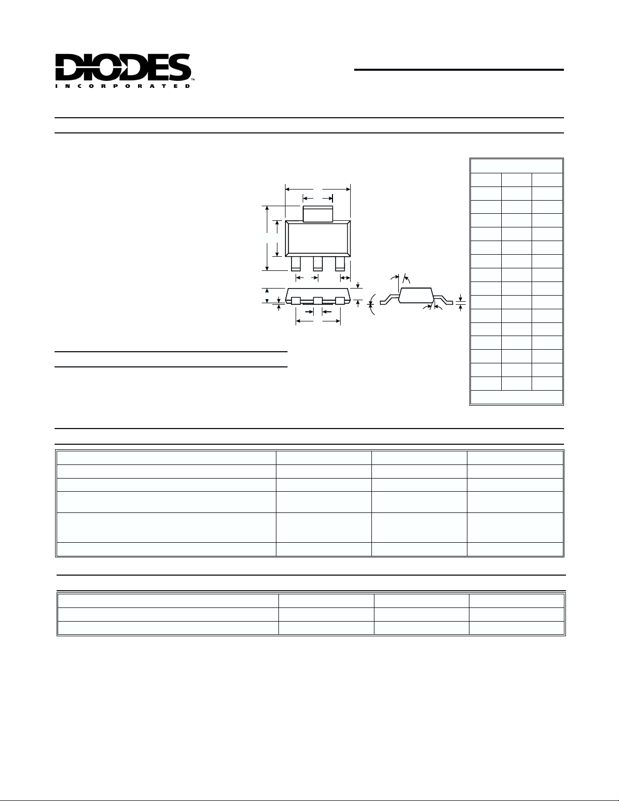
· SOT-223 Plastic Case
· Terminal Connections: See Outline Drawing
and Internal Circuit Diagram Above
C D
J
DT451N
N-CHANNEL ENHANCEMENT MODE
FIELD EFFECT TRANSISTOR
SOT-223
A
B
D
D
G
E
K
S
G
H
L
M
P
N
S
Dim Min Max
6.30 6.71
A
2.90 3.10
B
6.71 7.29
C
3.30 3.71
D
2.22 2.35
E
0.92 1.00
G
1.10 1.30
H
1.55 1.80
J
R
0.025 0.102
K
0.66 0.79
L
4.55 4.70
M
— 10°
N
10° 16°
P
0.254 0.356
R
10° 16°
S
All Dimensions in mm
Maximum Ratings
Drain-Source Voltage
Gate-Source Voltage
Drain Current Note 1a Continuous
Maximum Power Dissipation Note 1a
Operating and Storage Temperature Range
25°C unless otherwise specified
Characteristic Symbol Value Unit
Pulsed
Note 1b
Note 1c
Thermal Characteristics
Characteristic Symbol Value Unit
Thermal Resistance, Junction-to-Ambient Note 1
Thermal Resistance, Junction-to-Case
Notes: 1. R
is the sum of the junction-to-case and case-to-ambient thermal resistance where the case thermal reference is defined as
QJA
the solder mounting surface of the drain pins. R
1a. With 1 in
1b. With 0.0066 in2oz 2 oz. copper mounting pad R
1c. With 0.0123 in2oz 2 oz. copper mounting pad R
2
oz 2 oz. copper mounting pad R
V
DSS
V
GSS
I
D
P
d
T
j,TSTG
R
QJA
R
QJC
is guaranteed by design while R
QJC
QJA = 42°C/W.
QJA = 95°C/W.
QJA = 110°C/W.
30 V
±20 V
±5.5
±25
3.0
1.3
1.1
-65 to +150 °C
42 °C/W
12 °C/W
is determined by the user’s board design.
QCA
A
W
DS11607 Rev. C-4 1 of 4 DT451N

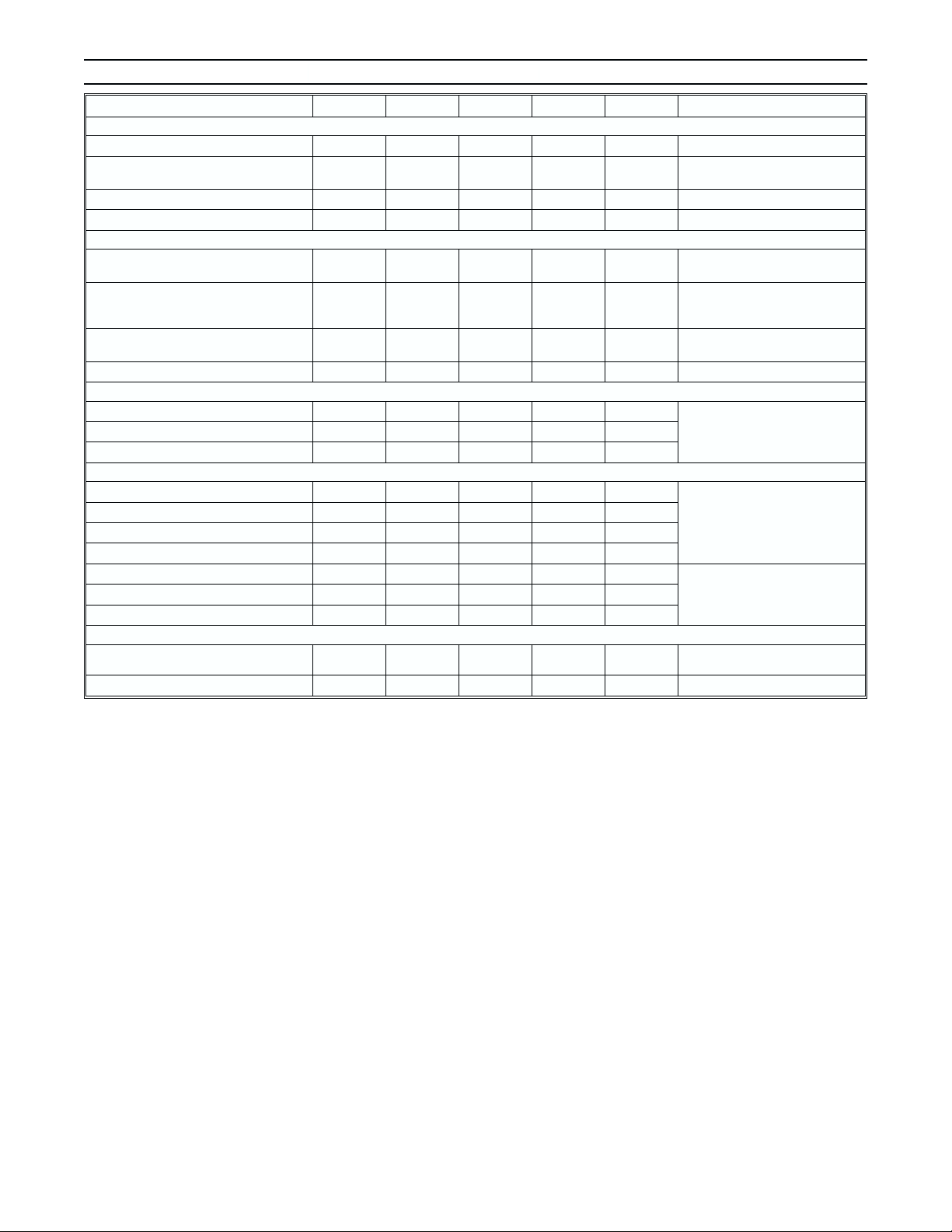
Electrical Characteristics
25°C unless otherwise specified
Characteristic Symbol Min Typ Max Unit Test Condition
OFF CHARACTERISTICS
Drain-Source Breakdown Voltage
Zero Gate Voltage Drain Current
T
j
Gate-Body Leakage, Forward
Gate-Body Leakage, Reverse
=55°C
BV
I
I
GSSF
I
GSSR
DSS
DSS
30 — — V
——
— — 100 nA
— — -100 nA
ON CHARACTERISTICS (Note 2)
Gate Threshold Voltage
T
= 125°C
j
Static Drain-Source On-Resistance
= 125°C
T
j
On-State Drain Current
Forward Transconductance
V
GS(th)
R
DS (ON)
I
D(ON)
g
FS
1.0
0.7
— 0.042
18
15
— 6.0 — m
DYNAMIC CHACTERISTICS
Input Capacitance
Output Capacitance
Reverse Transfer Capacitance
C
ISS
C
OSS
C
RSS
— 730 — pF
— 370 — pF
— 140 — pF
SWITCHING CHARACTERISTICS (Note 2)
Turn-On Delay Time
Turn-On Rise Time
Turn-Off Delay Time
Turn-Off Fall Time
Total Gate Charge
Gate-Source Charge
Gate-Drain Charge
t
D(ON)
t
t
D(OFF)
t
Q
Q
Q
—2030ns
r
—1525ns
—1940ns
f
g
gs
gd
—1030ns
—1625nC
— 1.8 3 nC
— 4.5 7.0 nC
DRAIN-SOURCE DIODE CHARACTERISTICS AND MAXIMUM RATINGS
Max Continuous Drain-Source Diode
Forward Current
Drain-Source Diode Forward Voltage
I
S
V
SD
— — 2.5 A
— 0.8 1.2 V
1.6
1.2
0.065
0.064
2.0
20
3.0
2.2
0.05
0.10
0.08
µA
V
W
—— A
= 0V, ID= 250µA
V
GS
VDS = 24V, V
= 20V, VDS= 0V
V
GS
= -20V, VDS= 0V
V
GS
V
DS=VGS
= 10V, ID= 5.5A
V
GS
V
= 4.5V, ID= 4.3A
GS
= 10V, VDS= 5.0V
V
GS
V
= 4.5V, VDS= 5.0V
GS
= 10V, ID= 5.5A
V
DS
= 10V, VGS= 0V
V
DS
f = 1.0MHz
V
= 15V, ID= 1.0A
DD
V
= 10V, R
GEN
V
= 10V. ID= 5.5A.
DS
V
= 10V
GS
= 0V, IS= 5.5A (Note 2)
V
GS
= 0V
GS
, ID= 250µA
GEN
= 6.0W
Notes: 2. Pulse Test: Pulse width l 300µs, duty cycle l 2.0%.
DS11607 Rev. C-4 2 of 4 DT451N
 Loading...