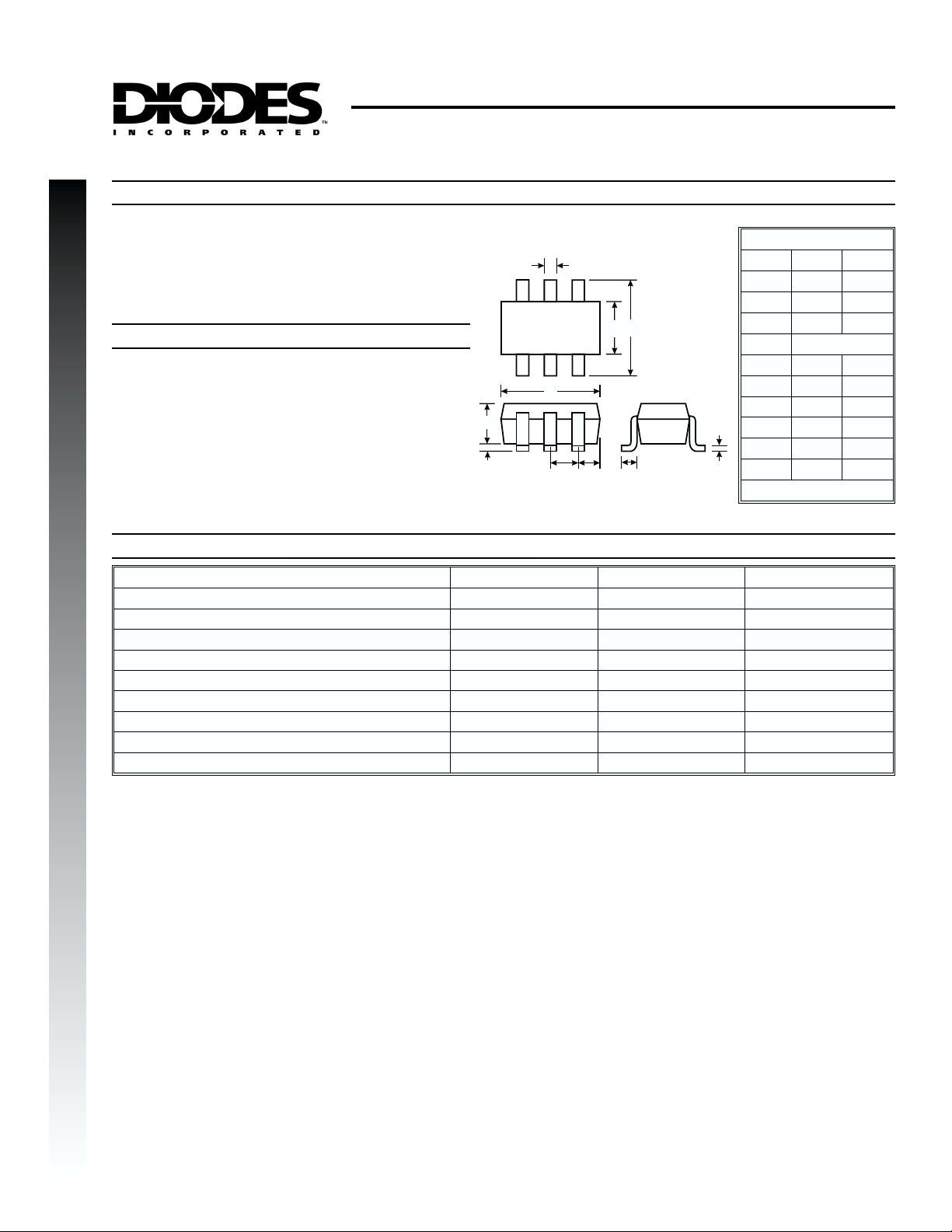
DIODS DMDT9922 Datasheet

Features
Epitaxial Planar Die Construction
·
Low Noise
·
High Current Gain
·
Matched Pair of Transistors
·
Mechanical Data
Case: SOT-363, Molded Plastic
·
Terminals: Solderable per MIL-STD-202,
·
Method 208
Terminal Connections: See Diagram
·
Marking: K3S
·
Weight: .006 grams (approx.)
·
ADVANCE INFORMATION
DMDT9922
PNP DUAL, MATCHED PAIR SURFACE MOUNT TRANSISTOR
SOT-363
Dim Min Max
A
B
C
D
F
H
J
M
K
L
M
All Dimensions in mm
0.10 0.30
1.15 1.35
2.00 2.20
0.65 Nominal
0.30 0.40
1.80 2.20
¾ 0.10
0.90 1.00
0.25 0.40
0.10 0.25
K
J
A
C2B1E
KXX
E2B2C
H
1
C
B
1
L
FD
Maximum Ratings
Characteristic Symbol DMDT9922 Unit
Collector-Base Voltage
Collector-Emitter Voltage
Emitter-Base Voltage
Collector-Collector Voltage
Emitter-Emitter Voltage
Collector Current - Continuous (Note 1)
Power Dissipation (Note 1)
Thermal Resistance, Junction to Ambient (Note 1)
Operating and Storage and Temperature Range
@ TA= 25°C unless otherwise specified
V
V
V
V
V
R
T
j,TSTG
CBO
CEO
EBO
CCO
EEO
I
C
P
d
qJA
-50 V
-40 V
-5.0 V
-50 V
-50 V
-100 mA
200
625 K/W
-55 to +125 °C
mW
UNAPPROVED
NOT FOR
DISTRIBUTION
DS30142 Rev. 1P-5 1 of 2 DMDT9922

Electrical Characteristics
Characteristic Symbol Min Typ Max Unit Test Condition
OFF CHARACTERISTICS (Note 2)
Collector-Base Breakdown Voltage
Collector-Emitter Breakdown Voltage
Emitter-Base Breakdown Voltage
Collector-Base Leakage Current
Emitter-Base Leakage Current
Collector-Emitter Leakage Current
ON CHARACTERISTICS (Note 2)
DC Current Gain
Collector-Emitter Saturation Voltage
Base-Emitter Impedance
Emitter-Base Offset Voltage
ADVANCE INFORMATION
Change in Emitter-Base Offset Voltage vs. Collector-Base
Voltage (CMRR)
Change in Emitter-Base Offset Voltage vs.
Collector-Current
Average Offset Voltage Drift
Emitter-Base Offset Current
Change in Emitter-Base Offset Current vs. Collector-Base
Voltage
Average Offset Current Drift
Collector-Collector Leakage Current
SMALL SIGNAL CHARACTERISTICS
Output Capacitance
Input Capacitance
Output Conductance
Current Gain-Bandwidth Product
@ TA= 25°C unless otherwise specified
V
(BR)CBO
V
(BR)CEO
V
(BR)EBO
I
CBO
I
EBO
I
CES
h
V
CE(SAT)
V
CE(SAT)
r
V
DV
DV
DV
DI
TC V
I
OS
DI
DV
TC I
I
CC
C
C
h
f
-50 ¾¾ V
-40 ¾¾ V
-5.0 ¾¾ V
¾ -0.3 -500 nA
¾¾-500 nA
¾ -4 -1000 nA
300 450 555 ¾
FE
¾
¾
be
OS
OS/
OS/
OS/
obo
ibo
OE
T
¾ -0.5 ¾W
¾ 10 ¾mV
¾ 10 ¾mV
CB
¾ 5 ¾mV
C
¾ 0.5 ¾mV/°C
OS
¾ 8 ¾ nA
¾ 30 ¾ nA
CB
¾ 50 ¾ pA/°C
OS
¾ 35 ¾ pA
¾¾70 pF
¾ 10 ¾mS
-0.1
-0.1
170 ¾ MHz
-0.5
¾
-4 15 pF
V
V
I
= -50mA, IE= 0
C
= -1.0mA, IB= 0
I
C
= -50mA, IC= 0
I
E
= -30V
V
CB
= -4.0V
V
EB
= -40V
V
CE
= -1.0mA, VCE= -6.0V
I
C
= -50mA, IB= -5.0mA
I
C
I
= -1mA, IB= -0.1mA
C
I
= -10mA to -1mA
C
= 0V, IC= -1mA to -1mA
V
CB
= 0V, IC= -1mA to -1mA
V
CB
= 0V, IC= -10mA to -1mA
V
CB
= -10mA to -1mA
I
C
= -10mA, VCB= 0V
I
C
= 0 to -50V
V
CB
I
= -10mA
C
= -40V
V
CE
= -10V, f = 1.0MHz, IE= 0
V
CB
= -0.5V, IC= 0, f = 1MHz
V
EB
= -1mA, VCE= -5V
I
C
= -12V, IC= -2.0mA,
V
CE
f = 100MHz
Notes: 1. Valid provided that terminals are kept at ambient temperature.
2. Pulse test: Pulse width £ 300ms, duty cycle £ 2%.
UNAPPROVED
NOT FOR
DISTRIBUTION
DS30142 Rev. 1P-5 2 of 2 DMDT9922
 Loading...