DIODS DMBT9922 Datasheet

Features
Epitaxial Planar Die Construction
·
Ideal for Medium Power Amplification and
·
Switching
High Current Gain
·
Complement to DMBT9022
·
Mechanical Data
Case: SOT-23, Molded Plastic
·
Terminals: Solderable per MIL-STD-202,
·
NEW PRODUCT
Method 208
Terminal Connections: See Diagram
·
Marking: K2S
·
Weight: 0.008 grams (approx.)
·
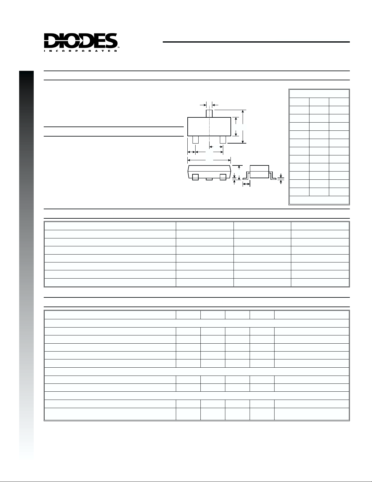
DMBT9922
PNP SMALL SIGNAL SURFACE MOUNT TRANSISTOR
SOT-23
Dim Min Max
A
B
C
D
E
G
H
M
J
K
L
M
All Dimensions in mm
0.37 0.51
1.19 1.40
2.10 2.50
0.89 1.05
0.45 0.61
1.78 2.05
2.65 3.05
0.013 0.15
0.89 1.10
0.45 0.61
0.076 0.178
E
TOP VIEW
B
A
C
B
C
E
D
G
H
K
J
L
Maximum Ratings
Characteristic Symbol DMBT9922 Unit
Collector-Base Voltage
Collector-Emitter Voltage
Emitter-Base Voltage
Collector Current - Continuous (Note 1)
Power Dissipation (Note 1)
Thermal Resistance, Junction to Ambient (Note 1)
Operating and Storage and Temperature Range
Electrical Characteristics
Characteristic Symbol Min Max Unit Test Condition
OFF CHARACTERISTICS (Note 2)
Collector-Base Breakdown Voltage
Collector-Emitter Breakdown Voltage
Emitter-Base Breakdown Voltage
Collector Cutoff Current
Emitter Cutoff Current
ON CHARACTERISTICS (Note 2)
DC Current Gain
Collector-Emitter Saturation Voltage
SMALL SIGNAL CHARACTERISTICS
Output Capacitance
Current Gain-Bandwidth Product
@ TA= 25°C unless otherwise specified
@ TA= 25°C unless otherwise specified
V
(BR)CBO
V
(BR)CEO
V
(BR)EBO
I
CBO
I
EBO
h
V
CE(SAT)
C
V
CBO
V
CEO
V
EBO
I
C
P
d
R
qJA
T
j,TSTG
-50 ¾ V
-40 ¾ V
-5.0 ¾ V
¾ -500 nA
¾ -500 nA
300 600 ¾
¾ -0.5 V
2.0 Typ. 3.5 pF
140 Typ. ¾ MHz
f
FE
obo
T
-50 V
-40 V
-5.0 V
-100 mA
225
556 K/W
-55 to +150 °C
= 50mA, IE= 0
-I
C
= 1.0mA, IB= 0
-I
C
= 50mA, IC= 0
-I
E
= -30V
V
CB
= -4.0V
V
EB
= -1.0mA, VCE= -6.0V
I
C
= -50mA, IB= -5.0mA
I
C
= -12V, f = 1.0MHz, IE= 0
V
CB
= -12V, IC= -2.0mA,
V
CE
f = 100MHz
mW
Notes: 1. Valid provided that terminals are kept at ambient temperature.
2. Pulse test: Pulse width £ 300ms, duty cycle £ 2%.
DS30126 Rev. 2P-5 1 of 1 DMBT9922
 Loading...