DIODS BYV28-50, BYV28-200, BYV28-150, BYV28-100 Datasheet

DS30033 Rev. A - PRELIMINARY 1 of 2 BYV28/50 - BYV28/200
BYV28/50 - BYV28/200
3.0A SUPER-FAST GLASS BODY RECTIFIER
Features
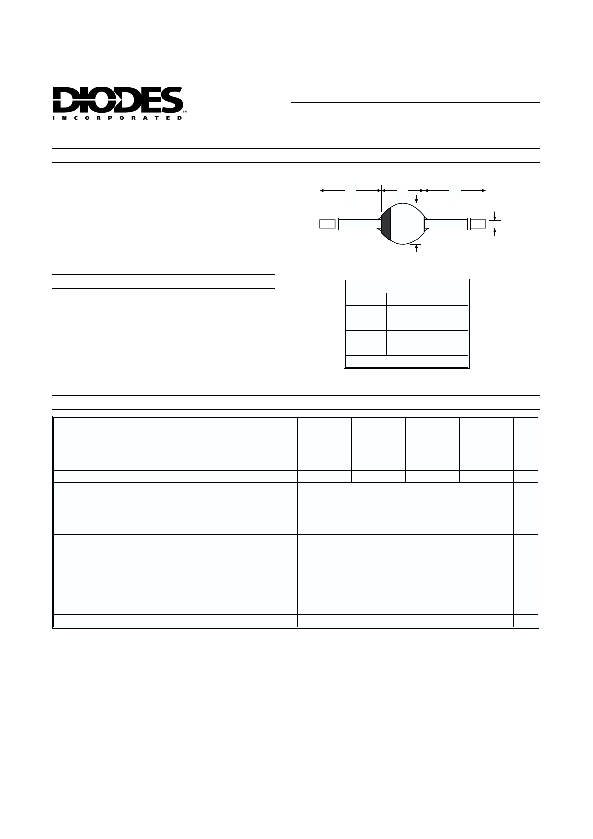
SOD-64
Dim Min Max
A 26.0 ¾
B ¾ 4.2
C ¾ 1.35
D ¾ 4.3
All Dimensions in mm
A A
B
C
D
Maximum Ratings and Electrical Characteristics
@Tj=25°C unless otherwise specified
·
Hermetically Sealed Glass Body Construction
·
Controlled Avalanche Characteristics
·
Super-Fast Switching for High Efficiency
·
High Current Capability and Low Forward
Voltage Drop
·
Surge Overload Rating to 90A Peak
·
Low Reverse Leakage Current
Mechanical Data
·
Case: SOD-64, Glass
·
Terminals: Plated Leads Solderable per
MIL-STD-202, Method 208
·
Polarity: Cathode Band
·
Weight: 1.0 grams (approx.)
· Mounting Position: Any
· Marking: Type Number
Characteristic Symbol BYV28/50 BYV28/100 BYV28/150 BYV28/200 Unit
Peak Repetitive Reverse Voltage
Working Peak Reverse Voltage
DC Blocking Voltage
V
RRM
V
RWM
V
R
50 100 150 200 V
RMS Reverse Voltage
V
R(RMS)
35 70 100 140 V
Non-Repetitive Peak Reverse Voltage
V
RSM
55 110 165 220 V
Average Rectified Output Current (Note 1)
I
O
3.5 A
Non-Repetitive Peak Forward Surge Current 8.3ms
single half sine-wave superimposed on rated load
(JEDEC Method)
I
FSM
90 A
Repetitive Forward Surge Current
I
FRM
25 A
Forward Voltage @ IF= 5.0A
V
FM
1.1 V
Peak Reverse Current @ Tj=25°C
at Rated DC Blocking Voltage @ T
j
= 165°C
I
RM
1.0
150
mA
Non-Repetitive Reverse Avalanche Energy
I
R
= 0.6A Inductive Load @ Tj= 175°C
E
RSM
20 mJ
Reverse Recovery Time (Note 2)
t
rr
30 ns
Typical Thermal Resistance Junction to Ambient (Note 1)
R
qJA
25 K/W
Operating and Storage Temperature Range
T
j,TSTG
-65 to +175 °C
Notes: 1.Leads maintained at ambient temperature at a distance of 10mm from the case.
2. Measured with I
F
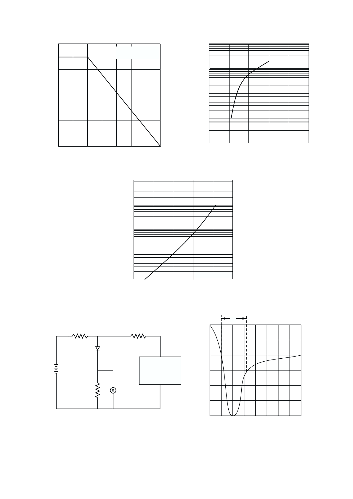
= 0.5A, IR= 1.0A, Irr= 0.25A. See Figure 4.

DS30033 Rev. A - PRELIMINARY 2 of 2 BYV28/50 - BYV28/200
0
1
2
3
4
0255075100 125 150 175
I , AVERAGE FWD RECTIFIED CURRENT (A)
(AV)
T , AMBIENT TEMPERATURE ( C)
Fi
g
. 1 Forward Current DeratingCurve
A
°
Single phase half wave
Resistive or Inductive load
0.1
1
10
100
0.01
0
I , INSTANTANEOUS FWD CURRENT (A)
F
V , INSTANTANEOUS FORWARD VOLTAGE (V)
Fi
g
.2 Typical Forward Characteristics
F
T = 25 Cj°
0.6 1.2 1.8 2.4 3.0
50V DC
Approx
50 NIΩ
50 NIΩ
1.0NIΩ
Oscilloscope
(Note 1)
Pulse
Generator
(Note 2)
Device
Under
Test
t
rr
Set time base for 50/100 ns/cm
+0.5A
0
-0.25A
-1.0A
Notes:
1. Rise Time = 7.0ns max. Input impedance = 1.0M , 22pF.
2. Rise Time = 10ns max. Input impedance = 50 .ΩΩ
Fig. 4 Reverse RecoveryTime Characteristic and Test Circuit
(+)
(+)
(-)
(-)
0.1
1
10
100
1000
0
I , REVERSE CURRENT ( A)
R
µ
T , Junction Temperature ( C)
Fi
g
.3 Typical Reverse Characteristics
j
°
V=V
R RRM
40 80 120 160 200
 Loading...