DIODS BAV99DW Datasheet

Features
Fast Switching Speed
·
Ultra-Small Surface Mount Package
·
For General Purpose Switching Applications
·
High Conductance
·
Two “BAV99” Circuits In One Package
·
Mechanical Data
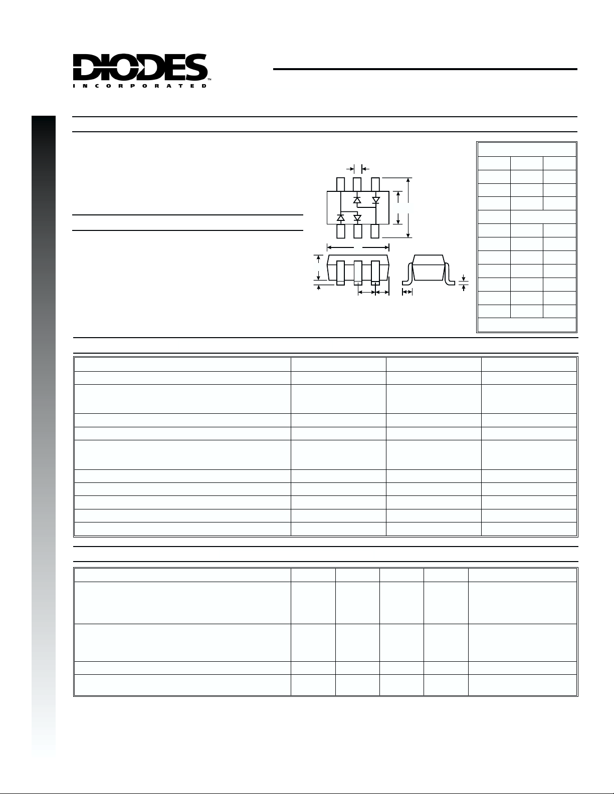
Case: SOT-363, Molded Plastic
·
Terminals: Solderable per MIL-STD-202,
·
NEW PRODUCT
Method 208
Polarity: See Diagram
·
Marking: KJG
·
Weight: 0.006 grams (approx.)
·
Case Material - UL Flammability Rating
·
Classification 94V-0
BAV99DW
QUAD SURFACE MOUNT SWITCHING DIODE ARRAY
SOT-363
A
AC
1
A
1
K
J
A
C
2
2
C
B
AC
C
1
2
H
L
FD
Dim Min Max
A
B
C
D
E
G
H
M
J
K
L
M
All Dimensions in mm
0.10 0.30
1.15 1.35
2.00 2.20
0.65 Nominal
0.30 0.40
1.80 2.20
1.80 2.20
¾ 0.10
0.90 1.00
0.25 0.40
0.10 0.25
Maximum Ratings
@ TA= 25°C unless otherwise specified
Characteristic Symbol BAV99DW Unit
Non-Repetitive Peak Reverse Voltage
Peak Repetitive Reverse Voltage
Working Peak Reverse Voltage
DC Blocking Voltage
RMS Reverse Voltage
Forward Continuous Current
Non-Repetitive Peak Forward Surge Current @ t = 1.0ms
@ t = 1.0ms
@ t = 1.0s
Power Dissipation (Note 1)
Thermal Resistance Junction to Ambient Air (Note 1)
Power Dissipation (Note 2)
Thermal Resistance Junction to Ambient Air (Note 2)
Operating and Storage Temperature Range
Electrical Characteristics
@ TA= 25°C unless otherwise specified
V
V
RRM
V
RWM
V
V
R(RMS)
I
I
FSM
P
R
P
R
T
j,TSTG
FM
RM
qJA
qJA
100 V
R
75
V
53 V
215 mA
2.0
1.0
0.5
d
200 mW
A
625 °C/W
d
300 mW
417 °C/W
-65 to +150 °C
Characteristic Symbol Min Max Unit Test Condition
I
= 1.0mA
F
I
= 10mA
F
I
= 50mA
F
I
= 150mA
F
= 75V
V
R
V
= 75V, Tj= 150°C
R
V
= 25V, Tj= 150°C
R
V
= 20V
R
= 0, f = 1.0MHz
V
R
= IR= 10mA,
I
F
I
= 0.1 x IR,RL= 100W
rr
Maximum Forward Voltage
Maximum Peak Reverse Current
Junction Capacitance
Reverse Recovery Time
0.715
V
FM
¾
0.855
1.0
V
1.25
2.5
I
RM
C
j
t
rr
¾
¾ 2.0 pF
¾ 4.0 ns
50
30
25
mA
mA
mA
nA
Notes: 1. Device mounted on FR-4 PCB, 1 inch x 0.85 inch x 0.062 inch; pad layout as shown on Diodes Inc. suggested pad layout
document AP02001, which can be found on our website at http://www.diodes.com/datasheets/ap02001.pdf.
2. Device mounted on Alumina PCB, 0.4 inch x 0.3 inch x 0.024 inch; pad layout as shown on Diodes Inc. suggested pad layout
document AP02001, which can be found on our website at http://www.diodes.com/datasheets/ap02001.pdf.
DS30145 Rev. C-2 1 of 3 BAV99DW

Ordering Information
(Note 3)
Device
BAV99DW-7
Notes: 3. For Packaging Details, go to our website at http://www.diodes.com/datasheets/ap02007.pdf.
Packaging Shipping
SOT-363 3000/Tape & Reel
Marking Information
NEW PRODUCT
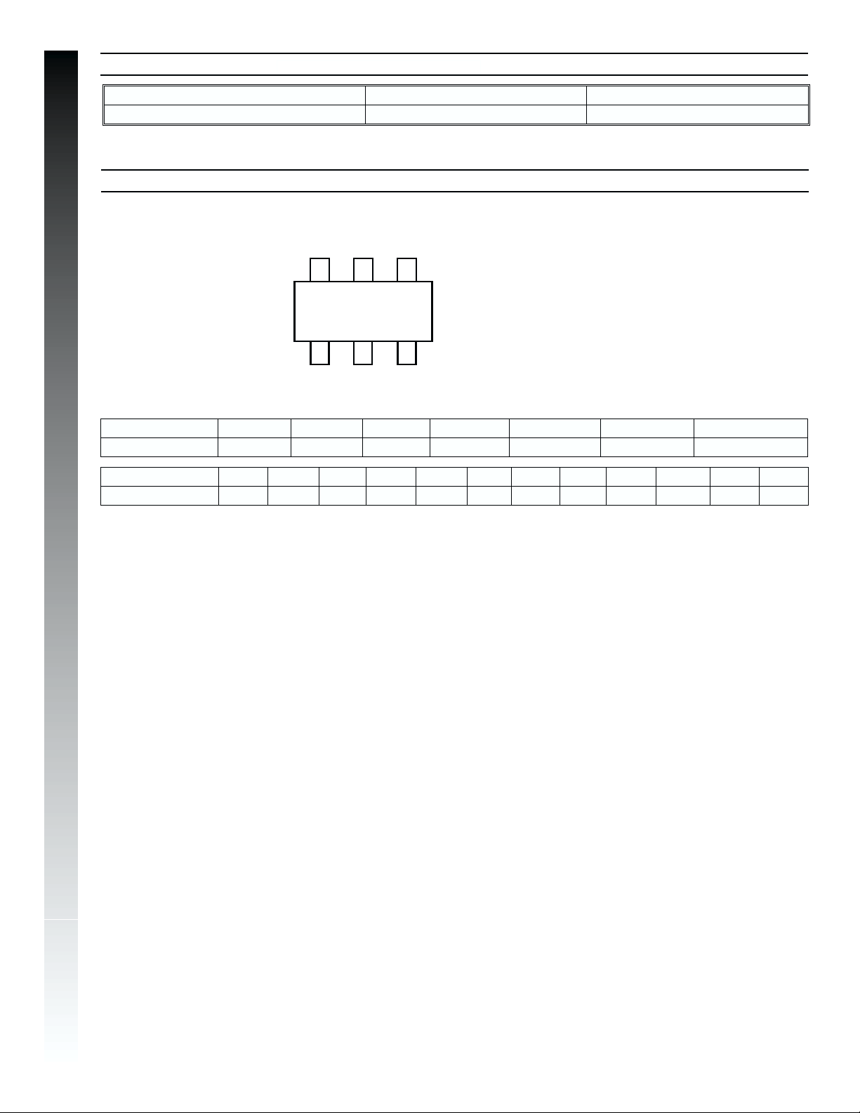
KJG = Product Type Marking Code
YM = Date Code Marking
Y = Year ex: N = 2002
M = Month ex: 9 = September
Date Code Key
Year 1998 1999 2000 2001 2002
Code
Month Jan Feb March Apr May Jun Jul
Code
KJG YM
JKLM N
1234567
KJG YM
2003 2004
OP
Aug Sep Oct Nov Dec
89 OND
DS30145 Rev. C-2 2 of 3 BAV99DW
 Loading...