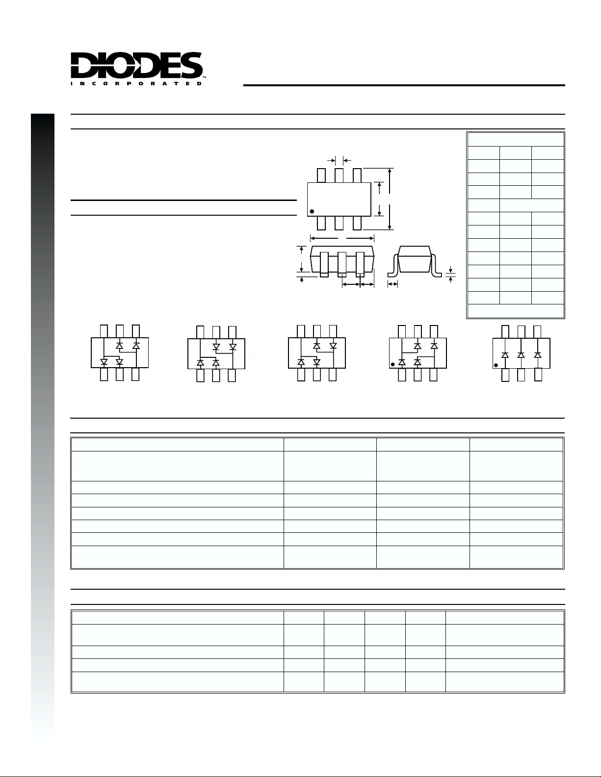
DIODS BAS70DW-06, BAS70DW-05, BAS70DW-04, BAS70BRW, BAS70TW Datasheet

Features
Low Forward Voltage Drop
·
Fast Switching
·
Ultra-Small Surface Mount Package
·
PN Junction Guard Ring for Transient and
·
ESD Protection
Mechanical Data
Case: SOT-363, Molded Plastic
·
Terminals: Solderable per MIL-STD-202,
·
NEW PRODUCT
Method 208
Orientation: See Diagrams Below
·
Weight: 0.006 grams (approx.)
·
BAS70TW /DW-04 /
DW-05 /DW-06 /BRW
SURFACE MOUNT SCHOTTKY BARRIER DIODE ARRAYS
SOT-363
A
C
B
H
K
J
L
FD
Dim Min Max
A
B
C
D
E
G
H
M
J
K
L
M
All Dimensions in mm
0.10 0.30
1.15 1.35
2.00 2.20
0.65 Nominal
0.30 0.40
1.80 2.20
1.80 2.20
¾ 0.10
0.90 1.00
0.25 0.40
0.10 0.25
A
1
C
1
2
2
A
C
2
1
BAS70DW-06*
Marking: K76
C
A
BAS70DW-05*
Marking: K71
A
A
2
2
1
C
A
2
1
1
C
C
*Symmetrical configuration, no orientation indicator.
Maximum Ratings
@ TA= 25°C unless otherwise specified
Characteristic Symbol Value Unit
Peak Repetitive Reverse Voltage
Working Peak Reverse Voltage
DC Blocking Voltage
RMS Reverse Voltage
Forward Continuous Current (Note 1)
Non-Repetitive Peak Forward Surge Current @ t < 1.0s
Power Dissipation (Note 1)
Thermal Resistance Junction to Ambient Air (Note 1)
Operating and Storage Temperature Range
Electrical Characteristics
@ TA= 25°C unless otherwise specified
AC
1
A
A
C
2
2
AC
C
1
1
2
BAS70DW-04*
Marking: K74
V
RRM
V
RWM
V
R
V
R(RMS)
I
FM
I
FSM
P
d
R
qJA
T
j
T
STG
AC
1
A
C
C
2
1
AC
A
2
1
2
BAS70BRW
Marking: K75
70 V
49 V
70 mA
100 mA
200 mW
625 K/W
-55 to +125
-65 to +125
C
C
2
1
A
A
2
1
BAS70TW
Marking: K73
°C
C
3
A
3
Characteristic Symbol Min Max Unit Test Condition
<300µs, IF= 1.0mA
Maximum Forward Voltage
Maximum Peak Reverse Current
Junction Capacitance
Reverse Recovery Time
V
FM
I
RM
C
j
t
rr
¾
¾ 100 nA
¾ 2.0 pF
¾ 5.0 ns
410
1000
mV
mV
t
p
t
<300µs, IF= 15mA
p
< 300µs, VR= 50V
t
p
= 0V, f = 1.0MHz
V
R
= IR= 10mA to IR= 1.0mA,
I
F
Irr = 0.1 x I
, RL= 100W
R
Notes: 1. Valid Provided that terminals are kept at ambient temperature.
DS30158 Rev. E-1 1 of 1 BAS70TW /DW-04 /DW-05 /DW-06 /BRW
 Loading...