DIODS BAS70-06, BAS70-04, BAS70, BAS70-05 Datasheet

Features
Low Turn-on Voltage
·
Fast Switching
·
PN Junction Guard Ring for Transient and
·
ESD Protection
Mechanical Data
Case: SOT-23, Molded Plastic
·
Terminals: Solderable per MIL-STD-202,
·
Method 208
Polarity: See Diagrams
·
Approx. Weight: 0.008 grams
·
BAS70/ -04/ -05/ -06
SURFACE MOUNT SCHOTTKY BARRIER DIODE
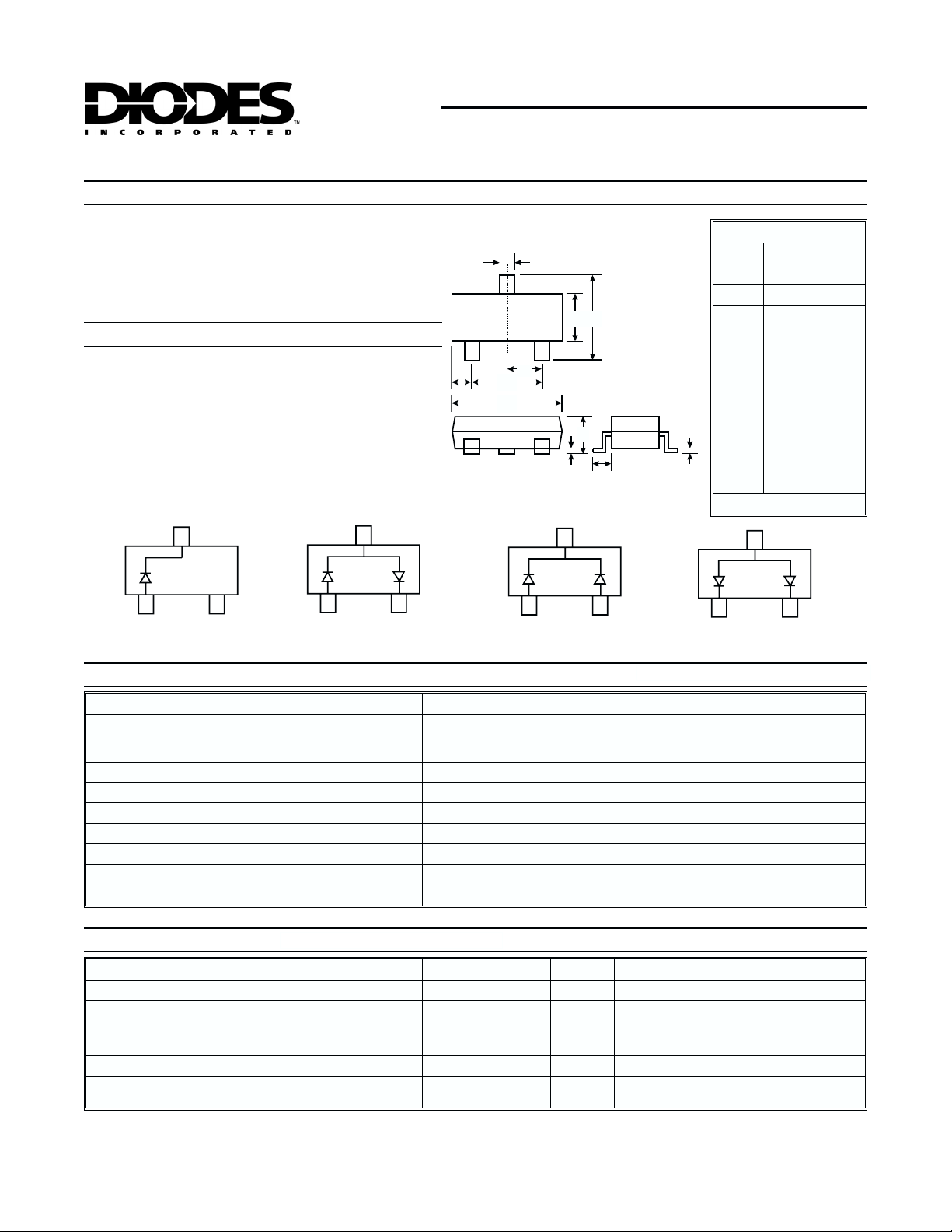
SOT-23
Dim Min Max
A
B
C
D
E
G
H
M
J
K
L
M
All Dimensions in mm
0.37 0.51
1.19 1.40
2.10 2.50
0.89 1.05
0.45 0.61
1.78 2.05
2.65 3.05
0.013 0.15
0.89 1.10
0.45 0.61
0.076 0.178
E
TOP VIEW
D
G
H
A
B
C
K
J
L
BAS70 Marking: K73, K7C
BAS70-04 Marking: K74, K7D BAS70-05 Marking: K75, K7E
Maximum Ratings and Electrical Characteristics, Single Diode
Characteristic Symbol BAS70 Unit
V
(BR)R
V
F
I
RM
C
j
t
rr
V
RRM
V
RWM
V
R
V
R(RMS)
I
F
I
FSM
P
d
R
qJA
T
j
T
STG
—
¾ 100 nA
¾ 2.0 pF
— 5.0 ns
-55 to +125 °C
-65 to +150 °C
410
1000
Peak Repetitive Reverse Voltage
Working Peak Reverse Voltage
DC Blocking Voltage
RMS Reverse Voltage
Forward Continuous Current (Note 1)
Non-Repetitive Peak Forward Surge Current @ tp< 1.0s
Power Dissipation (Note 1)
Thermal Resistance Junction to Ambient Air (Note 1)
Operating Junction Temperature Range
Storage Temperature Range
Electrical Ratings
Characteristic Symbol Min Max Unit Test Condition
Reverse Breakdown Voltage (Note 2)
Forward Voltage
Peak Reverse Current
Junction Capacitance
Reverse Recovery Time
@ TA= 25°C unless otherwise specified
BAS70-06 Marking: K76, K7F
@ TA= 25°C unless otherwise specified
70 V
49 V
70 mA
100 mA
200 mW
625 K/W
<300µs, IF= 1.0mA
t
mV
p
t
<300µs, IF= 15mA
p
< 300µs, VR= 50V
t
p
= 0V, f = 1.0MHz
V
R
= IR= 10mA to IR= 1.0mA,
I
F
R
=100W
L
Notes: 1. Valid Provided that terminals are kept at ambient temperature.
2. Test period <3000ms.
DS11007 Rev. L-2 1 of 1 BAS70/-04/-05/-06
 Loading...