DIODS BAS20W, BAS21W, BAS19W Datasheet

Features
· Fast Switching Speed
· Surface Mount Package Ideally Suited for
Automatic Insertion
· For General Purpose Switching Applications
· High Conductance
Mechanical Data
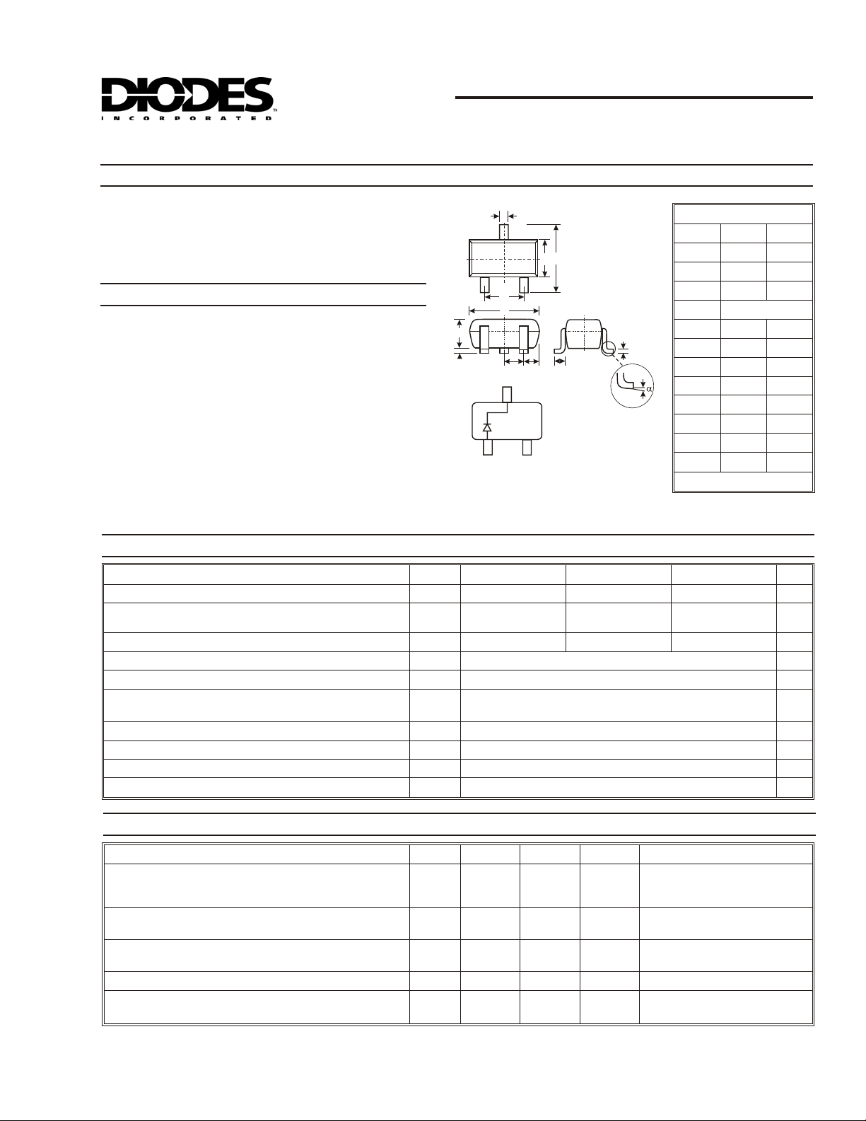
· Case: SOT-323, Molded Plastic
· Case Material - UL Flammability Rating
Classification 94V-0
· Moisture sensitivity: Level 1 per J-STD-020A
· Terminals: Solderable per MIL-STD-202,
Method 208
· Terminal Connections: See Diagram
· BAS19W Marking: KA8 or KT2 or KT3 (See Page 3)
· BAS20W Marking: KT2 or KT3 (See Page 3)
· BAS21W Marking: KT3 (See Page 3)
· Weight: 0.006 grams (approx.)
BAS19W - BAS21W
SURFACE MOUNT FAST SWITCHING DIODE
A
C
B
G
H
K
J
TOP VIEW
L
FD
M
SOT-323
Dim Min Max
0.25 0.40
A
1.15 1.35
B
2.00 2.20
C
0.65 Nominal
D
0.30 0.40
E
1.20 1.40
G
1.80 2.20
H
0.0 0.10
J
0.90 1.00
K
0.25 0.40
L
0.10 0.18
M
a 0° 8°
All Dimensions in mm
Maximum Ratings
@ TA= 25°C unless otherwise specified
Characteristic Symbol BAS19W BAS20W BAS21W Unit
Repetitive Peak Reverse Voltage
Working Peak Reverse Voltage
DC Blocking Voltage
RMS Reverse Voltage
Forward Continuous Current (Note 1)
Average Rectified Output Current (Note 1)
Non-Repetitive Peak Forward Surge Current @ t = 1.0ms
@ t = 1.0s
Repetitive Peak Forward Surge Current
Power Dissipation
Thermal Resistance Junction to Ambient Air (Note 1)
Operating and Storage Temperature Range
Electrical Characteristics
@ TA= 25°C unless otherwise specified
V
RRM
V
RWM
V
V
R(RMS)
I
I
FSM
I
FRM
P
R
Tj,T
FM
I
qJA
O
R
d
STG
120 200 250 V
100 150 200
71 106 141 V
400 mA
200
mA
2.5
0.5
625 mA
200 mW
625 °C/W
-65 to +150
V
A
°C
Characteristic Symbol Min Max Unit Test Condition
Reverse Breakdown Voltage (Note 2) BAS19W
BAS20W
BAS21W
Forward Voltage (Note 2)
Reverse Current
@ Rated DC Blocking Voltage (Note 2)
Total Capacitance
Reverse Recovery Time
V
(BR)R
V
F
I
R
C
T
t
rr
120
200
250
¾
¾
¾
¾
¾
¾
¾
1.0
1.25
100
15
5.0 pF
50 ns
nA
mA
V
V
I
= 100mA
R
= 100mA
I
F
= 200mA
I
F
= 25°C
T
j
T
= 100°C
j
V
= 0, f = 1.0MHz
R
IF = IR = 30mA,
= 0.1 x IR,RL = 100W
I
rr
Notes: 1. Part mounted on FR-4 PC board with minimum recommended pad layout, which can be found on our website at
http:/www.diodes.com/datasheets/ap02001.pdf.
2. Short duration test pulse used to minimize self-heating effect.
DS30118 Rev. 6 - 2 1 of 3 BAS19W - BAS21W
www.diodes.com

0
O
O
1
O
O
4
100
T = 150ºC
A
RWARD CURRENT (A)
US F
F
I , INSTANTANE
0.1
0.01
0.001
4.
3.5
3.0
2.5
T = -40ºC
A
T = 0ºC
A
T = 25ºC
A
T = 75ºC
A
T = 125ºC
1.0
A
1.2
T = 150ºC
A
0.2
0
V , INSTANTANEOUS FORWARD VOLTAGE (V)
F
0.4
0. 6
0.8
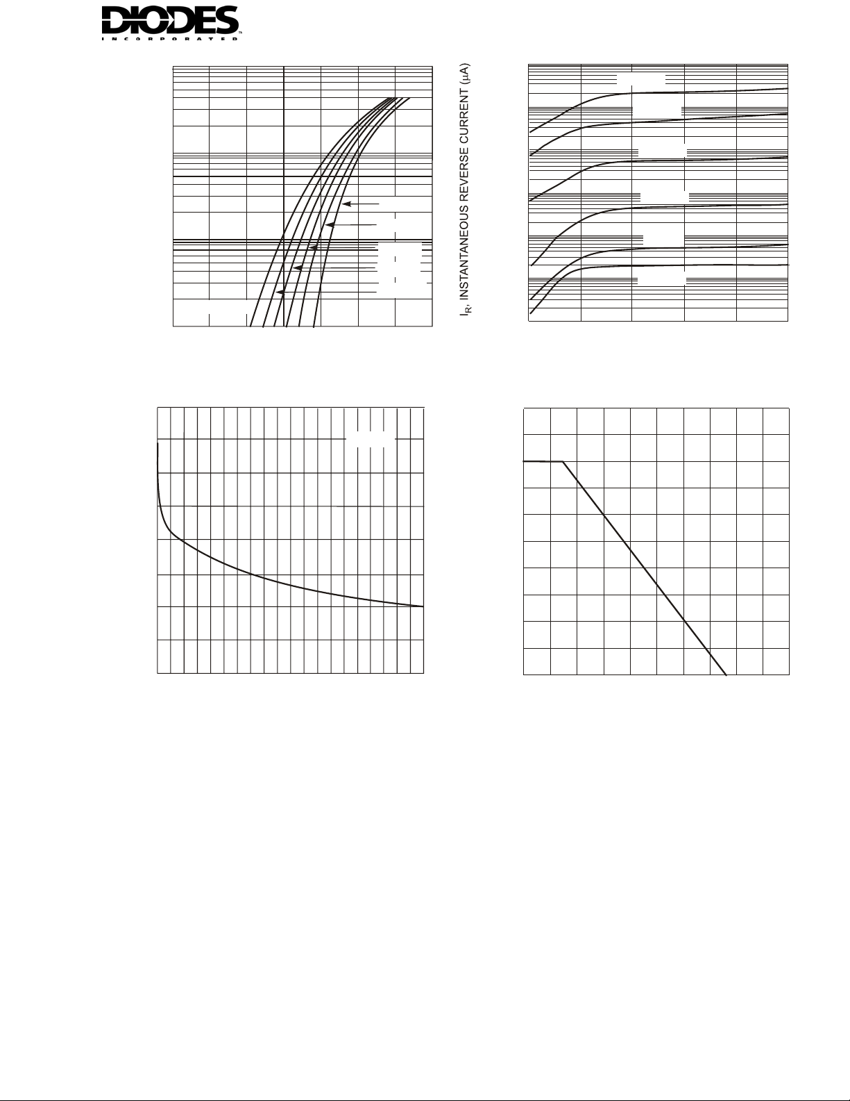
Fig. 1 Typical Forward Characteristics
f = 1.0MHz
10
1
0.1
0.01
0.001
T = 125ºC
A
T = 75ºC
A
T = 25ºC
A
T = 0ºC
A
T = -40ºC
A
0.0001
1.
0
V , INSTANTANEOUS REVERSE VOLTAGE (V)
50
R
100
150
200
250
Fig. 2 Typical Reverse Characteristics
250
200
N (mW)
150
2.0
1.5
100
WER DISSIPATI
1.0
T
C , TOTAL CAPACITANCE (pF)
0.5
0.0
0
10
V , REVERSE VOLTAGE (V)
R
20
Fig.3 Typical Capacitance vs. Reverse Voltage
30
40
P,P
50
d
0
0
T , AMBIENT TEMPERATURE (°C)
A
100 200
Fig. 4 Power Derating Curve, Total Package
DS30118 Rev. 6 - 2 2 of 3 BAS19W - BAS21W
www.diodes.com
 Loading...