DIODS B140N Datasheet

Features
Schottky Barrier Chip
·
Guard Ring Die Construction for Transient
·
Protection
Ideally Suited for Automatic Assembly
·
Low Power Loss, High Efficiency
·
Surge Overload Rating to 70A Peak
·
For Use in Low Voltage, High Frequency
·
Inverters, Free Wheeling, and Polarity
Protection Application
Plastic Material - UL Flammability
·
Classification 94V-0
Mechanical Data
Case: Molded Plastic
·
Terminals: Solder Plated Terminal -
·
ADVANCE INFORMATION
Solderable per MIL-STD-202, Method 208
· Polarity: Cathode Band or Cathode Notch
· Approx. Weight: 0.064 grams
· Mounting Position: Any
· Marking: Type Number
B140N
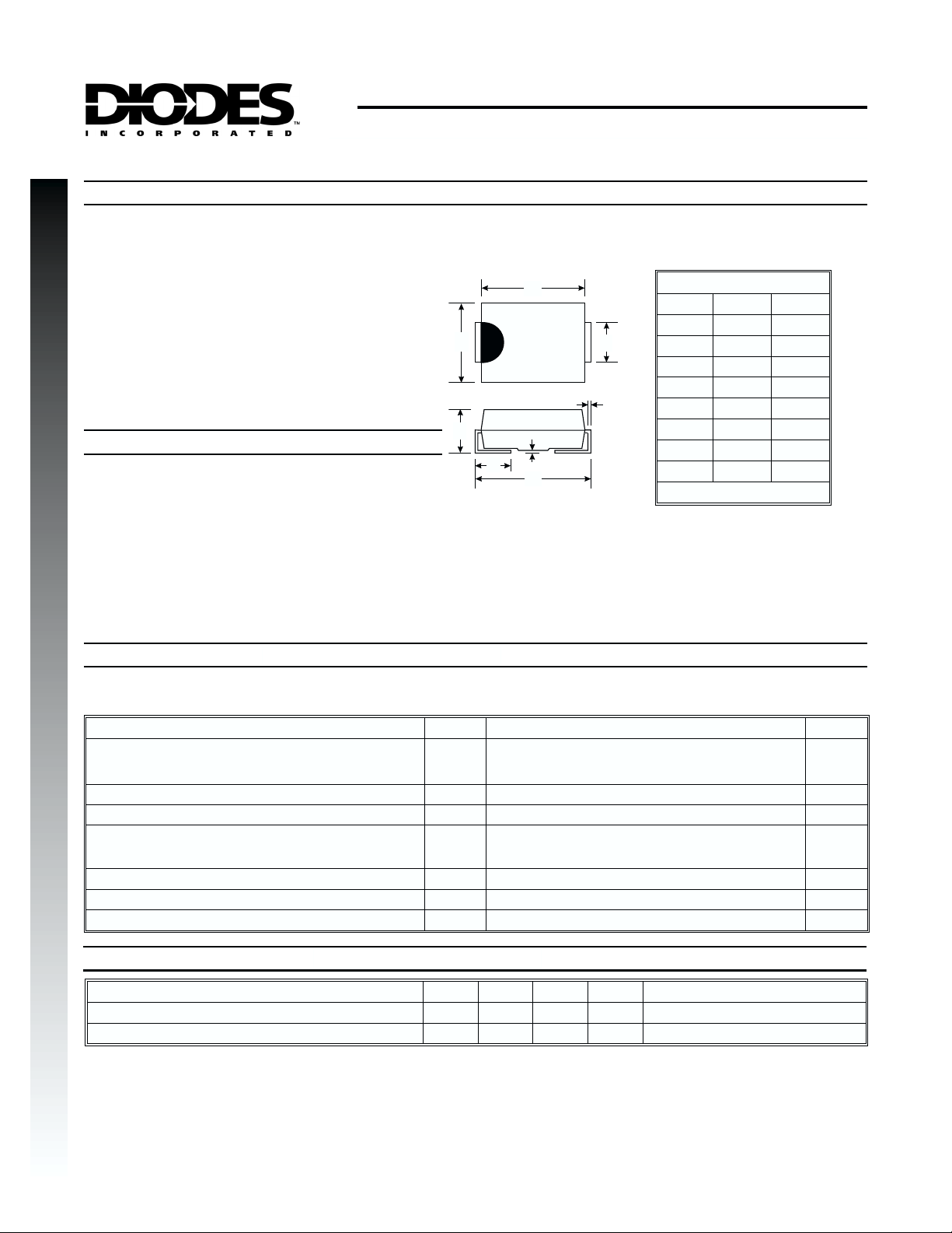
1.0A SURFACE MOUNT SCHOTTKY BARRIER RECTIFIER
B
Dim Min Max
A
A
J
H
G
E
C
D
B
C
D
E
G
H
J
All Dimensions in mm
SMA
2.29 2.92
4.00 4.60
1.27 1.63
0.15 0.31
4.80 5.59
0.10 0.20
0.76 1.52
2.01 2.62
Maximum Ratings
Single phase, half wave, 60Hz, resistive or inductive load.
For capacitive load, derate current by 20%.
Characteristic Symbol B140N Unit
Peak Repetitive Reverse Voltage
Working Peak Reverse Voltage
DC Blocking Voltage
RMS Reverse Voltage
Average Rectified Output Current (Note 3)
Non-Repetitive Peak Forward Surge Current, single half
sine-wave superimposed on rated load
(JEDEC Method)
Typical Junction Capacitance (Note 2)
Typical Thermal Resistance Junction to Terminal (Note 1)
Operating and Storage Temperature Range
Electrical Characteristics
Characteristic Symbol Typ Max Unit Conditions
Forward Voltage
Peak Reverse Current
Notes: 1. Thermal Resistance: Junction to terminal, unit mounted on PC board with 5.0 mm2(0.013 mm thick) copper pads as heat sink..
2. Measured at 1.0 MHz and applied reverse voltage of 4.0V DC.
3. When mounted on a PC board.
@ TA= 25°C unless otherwise specified
V
RRM
V
RWM
V
R
V
R(RMS)
I
O
I
FSM
C
j
R
qJT
T
j, TSTG
@ TA= 25°C unless otherwise specified
V
FM
I
RM
0.48 0.55 V
0.005 0.1 mA
40 V
28 V
1.0 A
70 A
60 pF
20 K/W
-40 to +125 °C
= 1.0A
I
F
= 40V
V
R
DS30136 Rev. A-0 1 of 2 B140N

10
g
100
1000
g
)
g
g
1.0
0.5
O,
I AVERAGE FORWARD CURRENT (A)
0
025
50
75 100 125
F
I , INSTANTANEOUS FORWARD CURRENT (A)
1
100m
125ºC
10m
75ºC
25ºC
1m
0 0.2 0.4 0.6 0.8 1.0
T , TERMINAL TEMPERATURE ( C)
ADVANCE INFORMATION
T
Fi
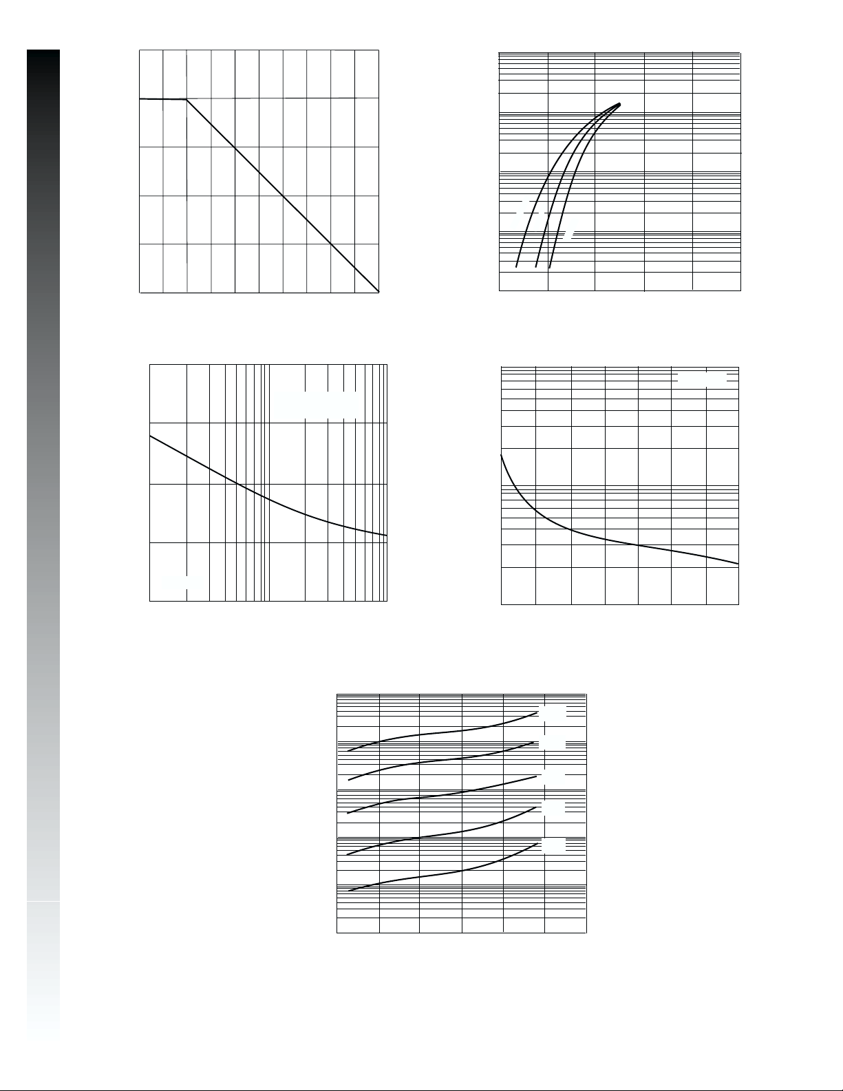
. 1 Forward Current DeratingCurve
75
50
25
T = 150ºC
j
0
I , PEAK FORWARD SURGE CURRENT (A)
FSM
1
NUMBER OF CYCLES AT 60 Hz
Fig. 3 Max Non-Repetitive Peak Fwd Surge Current
Single Half Sine-Wave
(JEDEC Method)
10
10m
°
V , INSTANTANEOUS FORWARD VOLTAGE (V)
F
Fi
.2 Typical Forward Characteristics
f=1MHz
100
J
C , JUNCTION CAPACITANCE (pF)
10
15
100
5
0
10
V , REVERSE VOLTAGE (V)
R
Fi
.4 Typical Junction Capacitance
125ºC
20
25
30
35
1m
100µ
10µ
100ºC
75ºC
50ºC
25ºC
1µ
R
100n
I , INSTANTANEOUS REVERSE CURRENT (A
20
10
0
V , REVERSE VOLTAGE (V)
R
Fi
.5 Typical Reverse Characteristics
30 40
50
60
DS30136 Rev. A-0 2 of 2 B140N
 Loading...