DIODS B0540W Datasheet

0.5A SURFACE MOUNT SCHOTTKY BARRIER RECTIFIER
Features
TCUDORPWEN
· Low Forward Voltage Drop
· Guard Ring Construction for
Transient Protection
· High Conductance
Mechanical Data
· Case: SOD-123, Plastic
· Case material - UL Flammability Rating
Classification 94V-0
· Moisture sensitivity: Level 1 per J-STD-020A
· Polarity: Cathode Band
· Leads: Solderable per MIL-STD-202,
Method 208
· Marking: Date Code & Type Code, See Page 2
· Type Code: Marking: SF
· Weight: 0.01 grams (approx.)
· Ordering Information, See Page 2
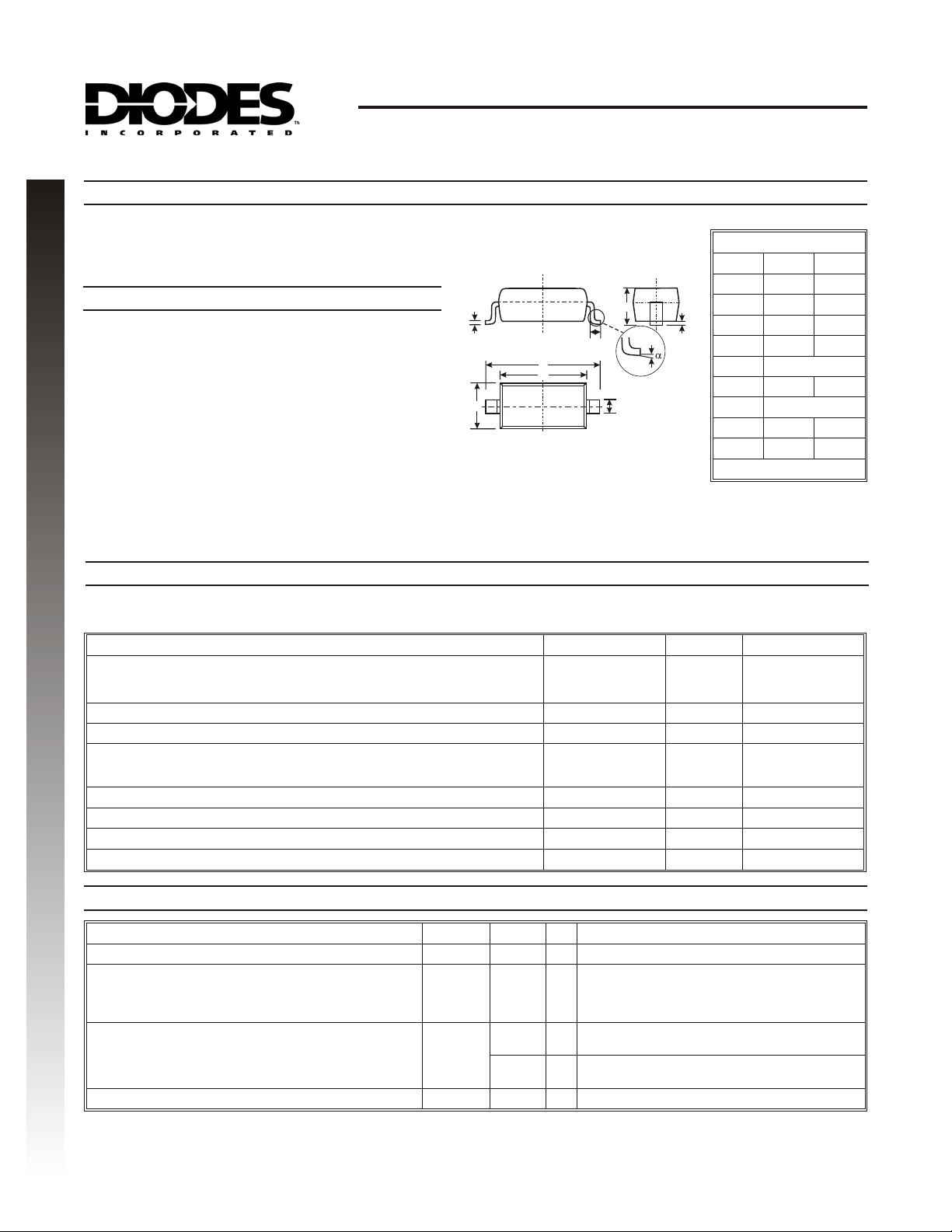
B0540W
SOD-123
Dim Min Max
A 3.55 3.85
H
A
B
C
D
G
E
J
B 2.55 2.85
C 1.40 1.70
D — 1.35
E 0.55 Typical
G 0.25 —
H 0.11 Typical
J — 0.10
a 0° 8°
All Dimensions in mm
Maximum Ratings
Single phase, half wave, 60Hz, resistive or inductive load.
For capacitive load, derate current by 20%.
Peak Repetitive Reverse Voltage
Working Peak Reverse Voltage
DC Blocking Voltage
RMS Reverse Voltage
Average Rectified Output Current @ TC = 115°C
Non-Repetitive Peak Forward Surge Current
8.3ms single half sine-wave superimposed on rated load
(JEDEC Method)
Power Dissipation (Note 1)
Typical Thermal Resistance Junction to Ambient (Note 1)
Operating and Storage Temperature Range
Voltage Rate of Change (Note 3)
Electrical Characteristics
Minimum Reverse Breakdown Voltage (Note 2)
Maximum Forward Voltage Drop
(Note 2)
Maximum Leakage Current
(Note 2)
Total Capacitance
Notes: 1. Device mounted on FR-4 PC board, 2"x2", 2 oz. Copper, single sided, Cathode pad dimensions 0.75"x1.0",
Anode pad dimensions 0.25"x1.0".
2. Pulse Test: Pulse width = 300ms, Duty Cycle £ 2%.
3. dv/dt measured at rated VR.
@ TA = 25°C unless otherwise specified
Characteristic Symbol B0540W Unit
V
RRM
V
RWM
V
R
V
R(RMS)
I
O
I
FSM
P
d
R
qJA
T
j,TSTG
dv/dt 1000 V/ms
@ TA = 25°C unless otherwise specified
Characteristic Symbol B0540W Unit Test Conditions
V
(BR)R
V
FM
I
RM
C
T
40 V
0.510
0.620
0.460
0.610
10
20
5.0
13
170 pF
V
mA
mA
40 V
28 V
0.5 A
5.5 A
410 mW
244 °C/W
-65 to +150 °C
IR = 20mA
= 0.5A, Tj = 25°C
I
F
= 1.0A, Tj = 25°C
I
F
I
= 0.5A, Tj = 100°C
F
= 1.0A, Tj = 100°C
I
F
= 20V, Tj = 25°C
V
R
V
= 40V, Tj = 25°C
R
VR = 20V, Tj = 100°C
VR = 40V, Tj = 100°C
f = 1MHz, V
= 0V DC
R
DS30138 Rev. 2 - 2 1 of 2 B0540W
www.diodes.com

5
00
G
C
C
(
)
10
1000
1.0
TCUDORPWEN
d
P , POWER DISSIPATION (mW)
400
300
200
100
0
025
1.0
50
75 100 125 150
T , AMBIENT TEMPERATURE (°C)
A
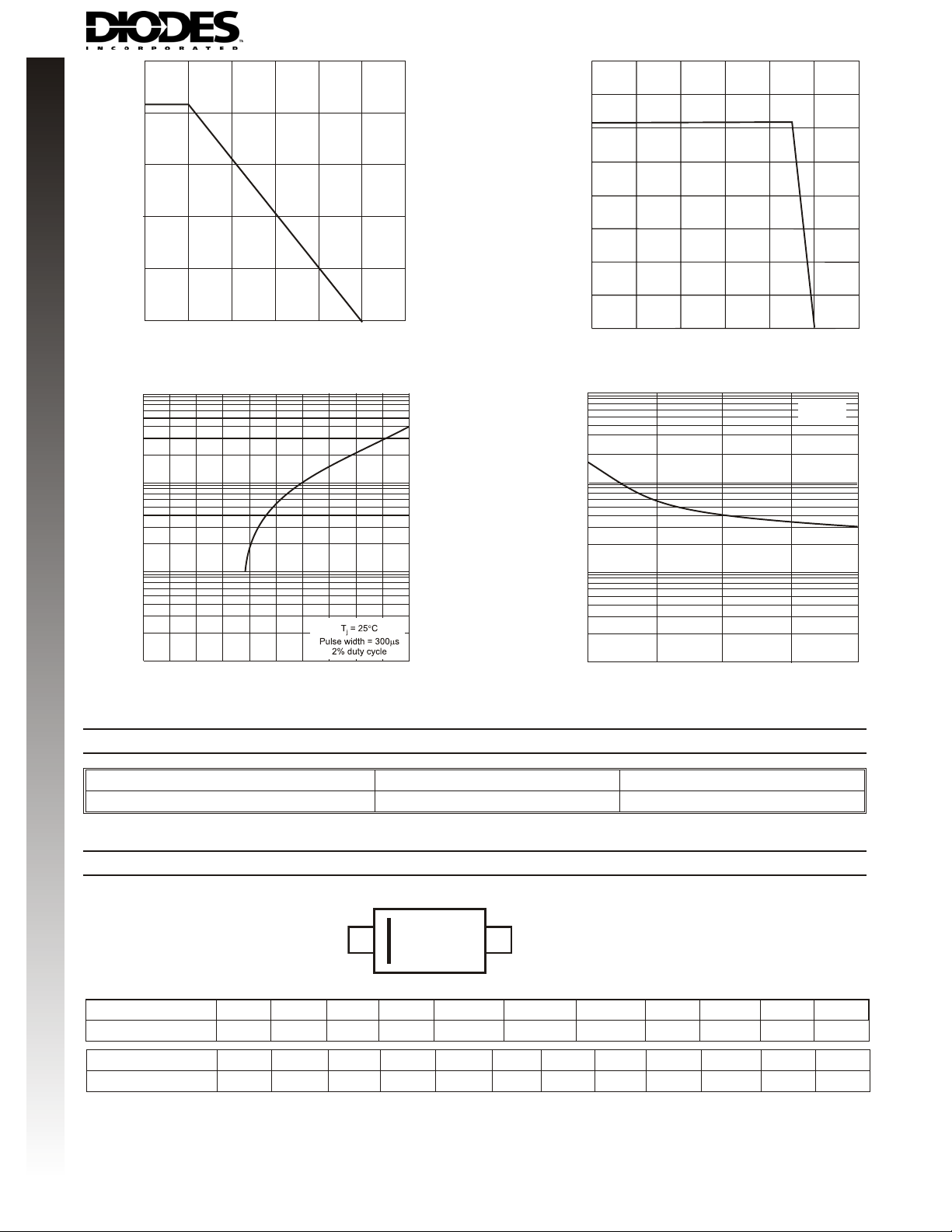
Fig. 1 Power Derating Curve
A
0.75
URRENT
0.50
TIFIED
ERE
0.25
O
I,AVERA
0
0 50 100 150
25 75 125
T , LEAD TEMPERATURE (° C)
L
Fig. 2 Forward Current Derating Curve
100
f=1MHz
0.1
T
C , TOTAL CAPACITANCE (pF)
F
I , INSTANTANEOUS FWD CURRENT (A)
0.01
0.200.40.60.81.0
V , INSTANTANEOUS FORWARD VOLTAGE (V)
F
Fig.3 Typical Forward Characteristics
Ordering Information
Device
B0540W-7
Notes: 4. For Packaging Details, go to our website at http://www.diodes.com/datasheets/ap02007.pdf.
(Note 4)
Packaging Shipping
SOD-123 3000/Tape & Reel
Marking Information
Date Code Key
Year 1998 1999 2000 2001 2002 2003
Code
Month Jan Feb March Apr May Jun Jul
Code
XX
JKLM N P
1234 567
XX = Product Type Marking Code (See Sheet 1)
YM = Date Code Marking
Y = Year (ex: N = 2002)
YM
M = Month (ex: 9 = September)
10
1.0
0 5 10 15 20
V , REVERSE VOLTAGE (V)
Fig.4 Typ. Total Capacitance vs Reverse Voltage
2004 2005 2006 2007 2008
R
RSTUV
Aug Sep Oct Nov Dec
89 OND
DS30138 Rev. 2 - 2 2 of 2 B0540W
www.diodes.com
 Loading...