DIODS 2N7002T Datasheet

Features
Drai
TCUDORPWEN
· Low On-Resistance
· Low Gate Threshold Voltage
· Low Input Capacitance
· Fast Switching Speed
· Low Input/Output Leakage
· Ultra-Small Surface Mount Package
Mechanical Data
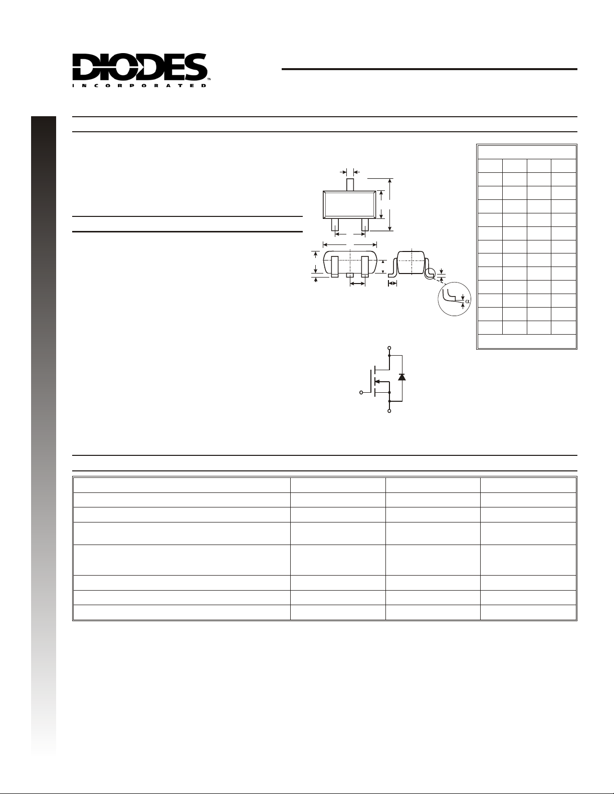
· Case: SOT-523, Molded Plastic
· Case Material UL Flammability Rating: 94V-0
· Moisture sensitivity: Level 1 per J-STD-020A
· Terminals: Solderable per MIL-STD-202,
Method 208
· Terminal Connections: See Diagram
· Marking: 72 (See Page 3)
· Weight: 0.002 grams (approx.)
· Ordering Information, see Page 3
2N7002T
N-CHANNEL ENHANCEMENT MODE FIELD EFFECT
TRANSISTOR
TOP VIEW
A
D
C
B
G
K
J
S
G
H
N
D
L
n
M
SOT-523
Dim Min Max Typ
A
0.15 0.30 0.22
B
0.75 0.85 0.80
C
1.45 1.75 1.60
D
¾¾0.50
G
0.90 1.10 1.00
H
1.50 1.70 1.60
J
0.00 0.10 0.05
K
0.60 0.80 0.75
L
0.10 0.30 0.22
M
0.10 0.20 0.12
N
0.45 0.65 0.50
a
0° 8°¾
All Dimensions in mm
Maximum Ratings
Characteristic Symbol Value Units
Drain-Source Voltage
Drain-Gate Voltage RGS£ 1.0MW
Gate-Source Voltage Continuous
Drain Current Continuous
Total Power Dissipation
Thermal Resistance, Junction to Ambient
Operating and Storage Temperature Range
@ TA = 25°C unless otherwise specified
Pulsed
Continuous @ 100°C
Pulsed
V
V
V
R
T
j,TSTG
DSS
DGR
GSS
I
D
P
qJA
Gate
Source
60 V
60 V
±20
±40
115
73
800
d
150
833 °C/W
-55 to +150
V
mA
mW
°C
DS30301 Rev. 2 - 2 1 of 3 2N7002T
www.diodes.com

Electrical Chacteristics
1
O
O
O
O
O
O
@ TA = 25°C unless otherwise specified
TCUDORPWEN
Characteristic Symbol Min Typ Max Unit Test Condition
OFF CHARACTERISTICS (Note 1)
Drain-Source Breakdown Voltage
Zero Gate Voltage Drain Current @ TC = 25°C
Gate-Body Leakage
ON CHARACTERISTICS (Note 1)
Gate Threshold Voltage
Static Drain-Source On-Resistance @ Tj = 25°C
On-State Drain Current
Forward Transconductance
DYNAMIC CHARACTERISTICS
Input Capacitance
Output Capacitance
Reverse Transfer Capacitance
SWITCHING CHARACTERISTICS
Turn-On Delay Time
Turn-Off Delay Time
Note: 1. Short duration test pulse used to minimize self-heating effect.
= 125°C
@ T
C
@Tj = 125°C
BV
I
I
V
GS(th)
R
DS (ON)
I
D(ON)
g
C
C
C
t
D(ON)
t
D(OFF)
DSS
DSS
GSS
FS
iss
oss
rss
60 ¾¾ V
¾¾
1.0
500
µA
¾¾±10 nA
1.0 ¾ 2.0 V
¾
2.0
4.4
7.5
13.5
0.5 1.0 ¾ A
80 ¾¾mS
¾ 22 50 pF
¾ 11 25 pF
¾ 2.0 5.0 pF
¾ 7.0 20 ns
¾ 11 20 ns
= 0V, ID = 10mA
V
GS
VDS= 60V, VGS = 0V
VGS = ±20V, VDS= 0V
= VGS, ID =-250mA
V
DS
V
= 5.0V, ID = 0.05A
GS
W
VGS = 10V, ID = 0.5A
VGS = 10V, VDS = 7.5V
=10V, ID = 0.2A
V
DS
= 25V, VGS= 0V
V
DS
f = 1.0MHz
V
= 30V, ID= 0.2A,
DD
R
= 150W,V
L
= 25W
R
GEN
GEN
= 10V,
V=5V
0.9
V = 10,7,6V
GS
0.8
0.7
0.6
0.5
0.4
0.3
D
I , DRAIN-SOURCE CURRENT (A)
0.2
0.1
0
012
V , DRAIN-SOURCE VOLTAGE (V)
DS
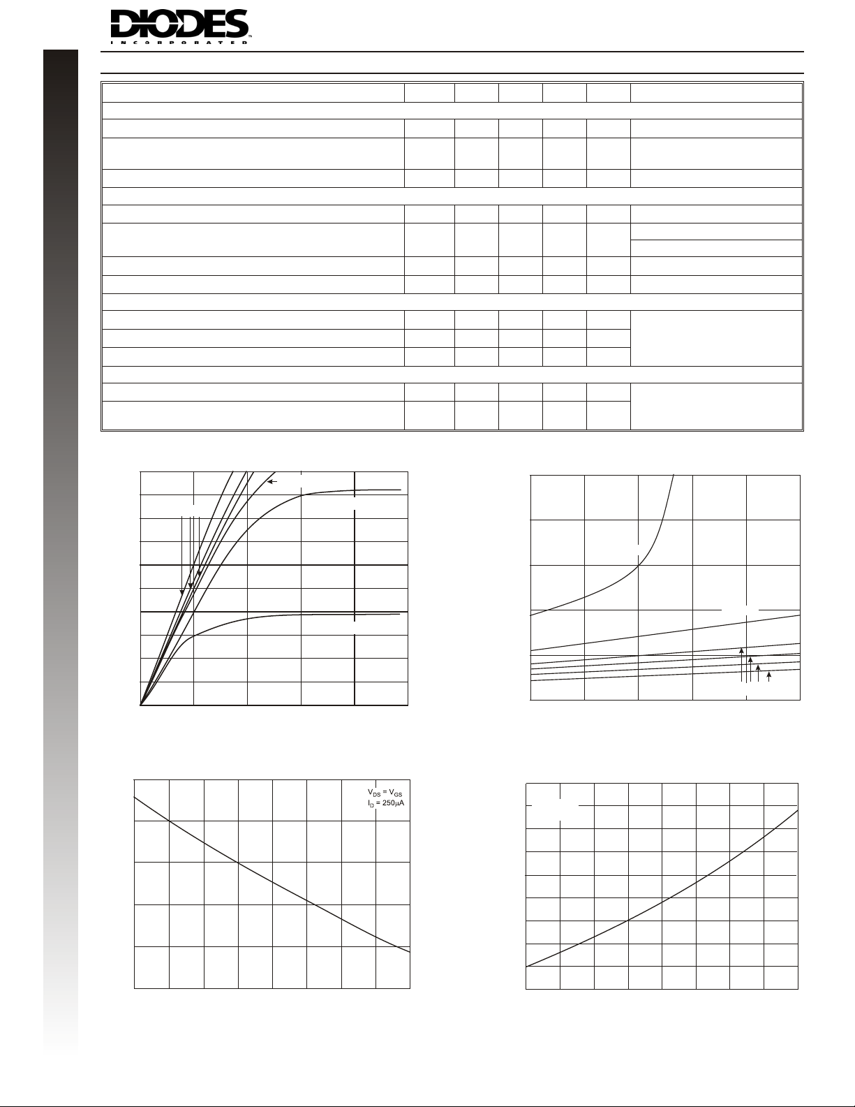
Fig. 1 On-Region Characteristics
1.2
LTAGE
1.1
LD V
1
0.9
RMALIZED THRESH
0.8
GS(th)
V,N
0.7
-50 -25
0
25
T , JUNCTION TEMPERATURE (° C)
J
Fig. 3 Gate Threshold Variation with Temperature
GS
V=4V
GS
2.2
V=3V
GS
1.8
RMALIZED
0.6
75
V=4V
GS
V = 5, 6, 7, 10V
GS
0.8
100
125 150
1.0
1.4
V=3V
GS
3
75
50
4
100 125
5
150
DS(ON)
R , N
DRAIN-SOURCE ON-RESISTANCE
1
0.6
00.2
Fig. 2 On-Resistance Variation with Gate Voltage and Drain-Source Current
2.2
V = 10V
2
GS
I = 500mA
D
1.8
1.6
N-RESISTANCE
1.4
1.2
1
RMALIZED
0.8
DS(ON)
0.6
R,N
0.4
-50 -25
T , JUNCTION TEMPERATURE (°C)
Fig. 4 On-Resistance Variation with Temperature
0.4
I , DRAIN-SOURCE CURRENT (A)
D
02550
J
DS30301 Rev. 2 - 2 2 of 3 2N7002T
www.diodes.com
 Loading...