diodes incorporated AP8801 Service Manual

AP8801
500mA LED Step-down Converter
Features
• LED driving current up to 500mA
• Operating input voltage up to 48V
• High efficiency up to 92%
• High switching frequency up to 500kHz
• PWM/DC input for dimming control
• Built-in output open-circuit protection
• SOP-8L and MSOP-8L are available in “Green”
Molding Compound (No Br, Sb)
• Lead Free Finish/RoHS Compliant (Note 1)
Applications
• Commercial & industrial lighting
• Small LCD panel backlight
• Appliances interior lighting
• Architecture Detail lighting
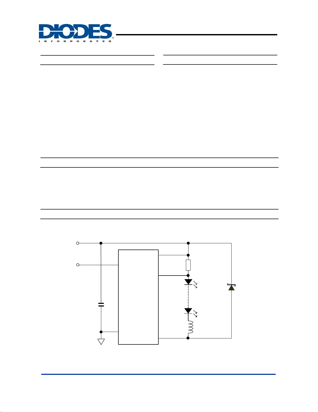
Typical Application Circuit
General Description
The AP8801 is a step-down DC/DC converter designed to drive
LEDs with a constant current. The device can drive up to thirteen
LEDs, depending on the forward voltage of the LEDs, in series
from a voltage source of 8V to 48V. Series connection of the
LEDs provides identical LED currents resulting in uniform
brightness and eliminating the need for ballast resistors. The
AP8801 switches at f requency up to 500kHz. This allows the
use of small size external components, hence minimizing the
PCB area needed.
Maximum output current of AP8801 is set via an external resistor
connected between the V
achieved by applying either a DC voltage or a PWM signal at the
CTRL input pin. An input voltage of 0.2V or lower at CTRL shuts
down the output at SW and puts the device into a low-current
standby state.
and SET input pins. Dimming is
IN
24V_DC
V
IN
R
CTRL
SET
SET
= 0.43Ω
1
D
1
AP8801
C1= 2.2μF
GND
SW
Figure 1: Typical Application Circuit
AP8801 Rev. 4 1 of 11 DECEMBER 2009
DS31765 www.diodes.com © Diodes Incorporated
L1= 100μH

Ordering Information
AP8801
500mA LED Step-down Converter
AP 8801 XX G - 13
Package Packing
S : SOP-8L
M8 : MSOP-8L
Device
AP8801SG-13 S SOP-8L 2500/Tape & Reel -13
AP8801M8G-13 M8 MSOP-8L 2500/Tape & Reel -13
Notes: 1. EU Directive 2002/95/EC (RoHS). All applicable RoHS exemptions applied. Please visit our website at
http://www.diodes.com/datasheets/ap02001.pdf.
http://www.diodes.com/products/lead_free.html.
2. Pad layout as shown on Diodes Inc. suggested pad layout document AP02001, which can be found on our website at
Package
Code
Packaging
(Note 2)
Green
G : Green
13 : Tape & Reel
13” T ape and Reel
Quantity Part Number Suffix
Pin Assignments
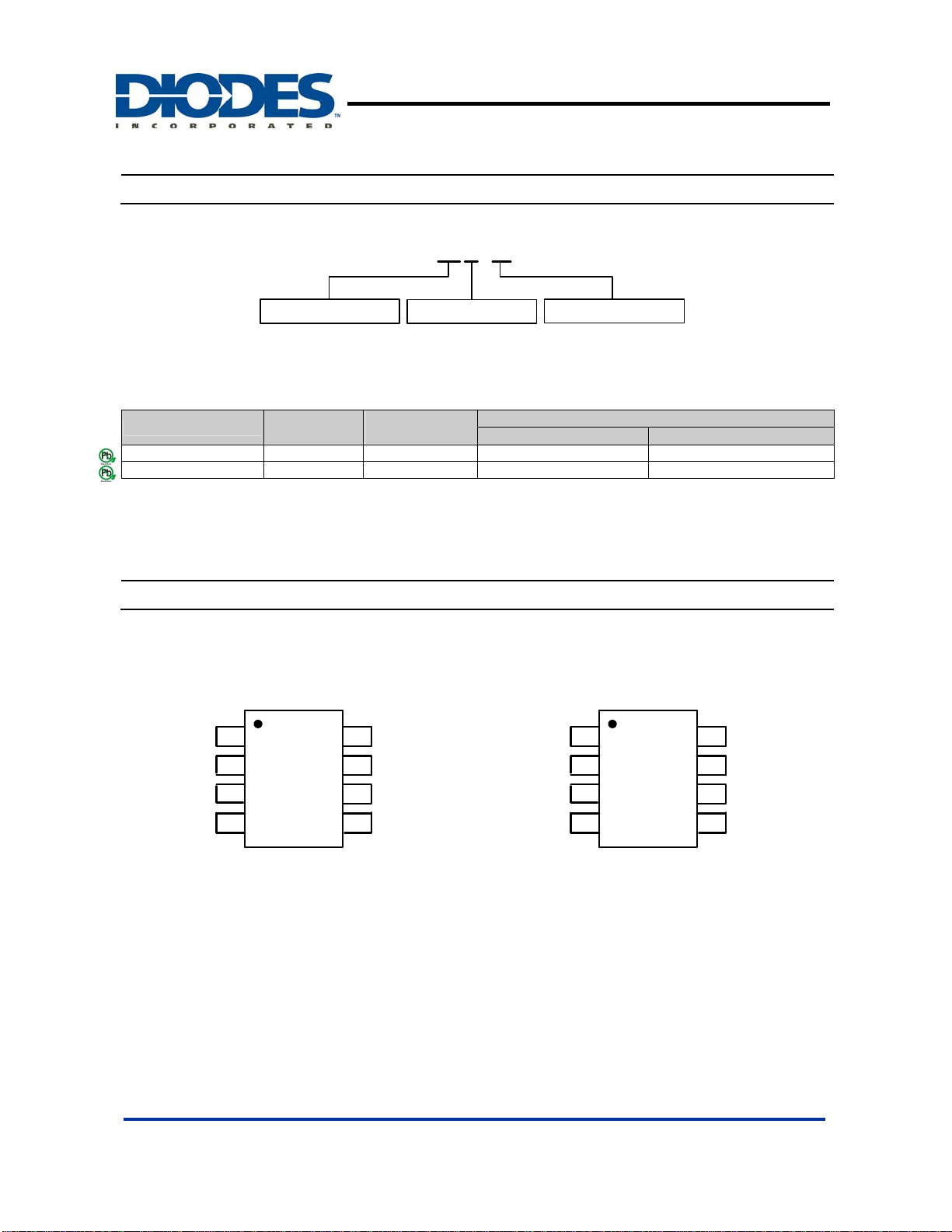
(1) SOP-8L (2) MSOP-8L
SET
( Top View )
1
8
CTRL
SET
( Top View )
1
8
CTRL
GND GND
NC
AP8801 Rev. 4 2 of 11 DECEMBER 2009
DS31765 www.diodes.com © Diodes Incorporated
2
AP8801
3
45
V
IN
7
6
SW
SW
GND GND
NC
2
AP8801
3
45
V
IN
7
6
SW
SW

500mA LED Step-down Converter
Pin Descriptions
Pin Name Description
SW
GND GND pin
SET Set Nominal Output Current Pin. Configure the output current of the device.
CTRL
VIN Input Supply Pin. Must be locally bypassed.
NC No connection
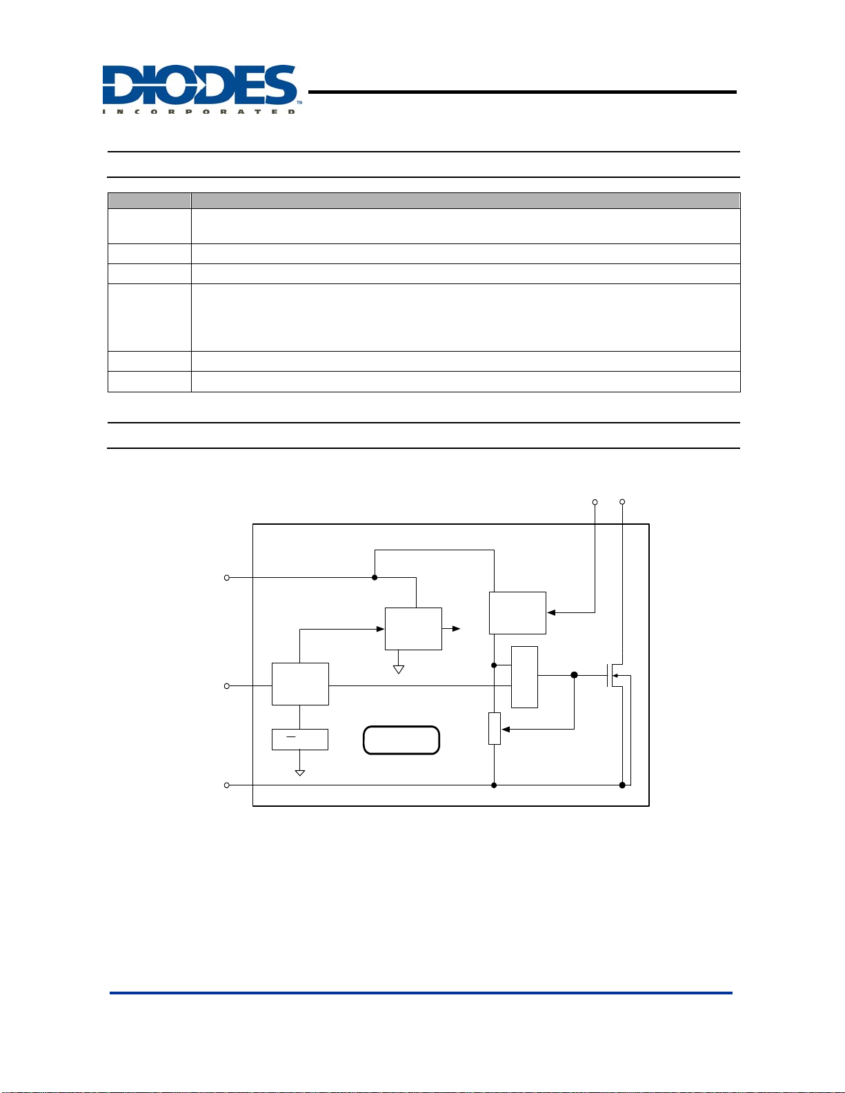
Block Diagram
Switch Pin. Connect inductor/freewheeling diode here, minimizing track length at this pin to
reduce EMI.
Dimming and On/Off Control Input. Input voltage of 0.2V or lower forces the device into low
current standby mode and shuts off the output. A PWM signal allows the output current to be
adjusted above or below the level set by the resistor connected to SET input pin.
The input impedance is about 50kΩ, and if the pin is left open V
CTRL
= V
SET
AP8801
REF
SW
V
CTRL
GND
IN
Sensing
5V
Block
Comparator
R
PWM/DC
Control
1.25V
V
REF
Voltage
Regulator
AP8801
Figure 2: AP8801 Block Diagram
AP8801 Rev. 4 3 of 11 DECEMBER 2009
DS31765 www.diodes.com © Diodes Incorporated

AP8801
500mA LED Step-down Converter
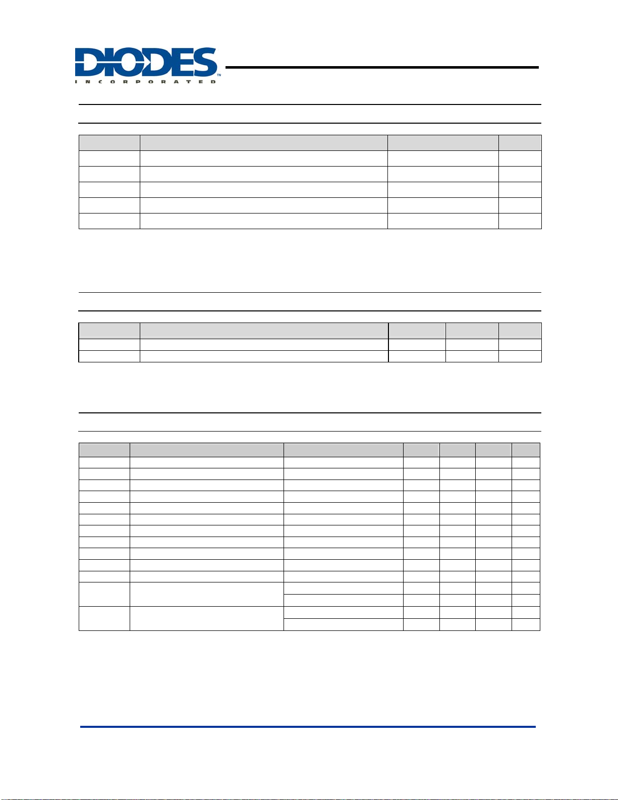
Absolute Maximum Ratings
Symbol Parameter Rating Unit
VIN VIN pin voltage -0.3~50 V
VSW SW voltage -0.3~50 V
TJ Junction Temperature 150
T
Lead Temperature Soldering 300
LEAD
T
Storage Temperature Range -65 to +150
ST
Caution: The absolute maximum ratings are rated values exceeding which the product could suffer physical damage. These values must therefore not
be exceeded under any condition.
Semiconductor devices are ESD sensitive and may be damaged by exposure to ESD events. Suitable ESD precautions should be taken
when handling and transporting these devices
Recommended Operating Conditions
Symbol Parameter Min Max Unit
TA Ambient Temperature Range -40 105 ºC
Duty Cycle Using Inductor ≥ 100µH (Note 3) 0.1 0.95
Notes: 3. For most applications the LED current will be within 8% over the duty cycle range specified. Duty cycle accuracy is also dependent on
Electrical Characteristics (V
Symbol Parameter Conditions Min Typ. Max Unit
Rds(on) On Resistance of MOSFET ISW=0.4A 0.7 1.15 Ω
I
SW Leakage
Notes: 4. Refer to figure 6 for the device derating curve.
propagation delay. Smaller size inductors can be used but LED current accuracy may be greater than 8% at extremes of duty cycle. This is
most noticeable at low duty cycles (less than 0.1) or when the input voltage is high and only one LED is being driven.
=24V, TA=25oC, unless otherwise specified)
IN
VIN Operating Input Voltage 8.0 - 48 V
I
Continuous switch current (Note 4) 500 mA
OUT
IQ Quiescent Current - 78 120 μA
F
Switching Frequency - - 0.5 MHz
OSC
V
Internal Threshold Voltage 184 200 216 mV
THD
V
Internal Reference Voltage - 1.25 - V
REF
SET SET pin input current V
-0.2 - 7 - μA
SET=VIN
Switch leakage current - - 8 μA
EN Voltage High ON 1.25 - - V
EN Voltage Low OFF - - 0.2 V
θ
θ
Thermal Resistance
JA
Junction-to-Ambient
Thermal Resistance
JC
Junction-to-Case
5. Test condition for SOP-8L and MSOP-8L: Device mounted on FR-4 PCB, 2”x2”, 2oz copper, minimum recommended pad layout on top layer
and thermal vias to bottom layer ground plane. For better thermal performance, larger copper pad for heat-sink is needed.
SOP-8L (Note 5) - 88 MSOP-8L (Note 5) - 128 SOP-8L (Note 5) - 58 MSOP-8L (Note 5) - 90 -
o
C
o
C
o
C
°C/W
°C/W
°C/W
°C/W
AP8801 Rev. 4 4 of 11 DECEMBER 2009
DS31765 www.diodes.com © Diodes Incorporated
 Loading...